Note: Descriptions are shown in the official language in which they were submitted.
2û78636
DEMODULATOR FOR CONTINUOUSLY AND ACCURATELY
CARRYING OUT DEMODULATING OPERATION BY A
FREQUENCY MULTIPLICATION METHOD
Background of the Invention:
This invention relates to a demodulator circuit
and, in particular, to a synchronous-detection
demodulator circuit which is widely used in various
5 communication systems, for example, in a mobile
communication system.
In the mobile communication system, it is
necessary to use a modulation and demodulation device
(modem) for carrying out burst operation. This is
10 because communication is frequently interrupted in the
mobile communication system. The modem comprises
modulator and demodulator circuits which will be
described in the following.
The modulator circuit is for modulating an
15 original analog signal by phase-modulating a plurality of
phases of a particular number into a modulated signal
having a particular frequency. The modulated signal is
used as a carrier in the mobile communication system in
the manner known in the art.
The demodulator circuit is for demodulating the
modulated signal into a demodulated signal. The
2 2078636
demodulated signal is a reproduction of the original
analog signal.
In the manner which will later be described, a
conventional demodulator circuit comprises a signal
converting circuit, a frequency multiplier, a signal
processing circuit, a frequency demultiplier, and a
signal producing circuit.
The signal converting circuit is for converting
the modulated signal into a digital signal. The
frequency multiplier is for multiplying the particular
frequency by the particular number to produce a
multiplied signal. The signal processing circuit is for
processing the multiplied signal into a modified signal
of a multiplied frequency. The frequency demultiplier is
for demultiplying the multiplied frequency by the
particular number to produce a demultiplied signal of the
particular frequency. The signal producing circuit is
for producing the demodulated signal in accordance with
the digital and the demultiplied signals.
The conventional demodulator circuit has a
disadvantage in that it is difficult to continuously and
accurately carry out demodulating operation as will later
be discussed in detail.
Summary of the Invention:
It is therefore an object of this invention to
provide a demodulator circuit in which demodulating
operation is continuously and accurately carried by a
frequency multiplication method.
.
- 2078636
--3--
Other objects of this invention will become clear as
the description proceeds.
According to this invention, there is provided a
demodulator circuit for demodulating a modulated signal into a
demodulated signal, said modulated signal being derived by
phase-modulating in m phases an original analog signal and
having a particular frequency, said demodulated signal being a
reproduction of said analog signal, said demodulator circuit
comprising a signal converting circuit for converting said
modulated signal into a digital signal, a frequency multiplier
for multiplying said particular frequency by m to produce a
multiplied signal, a signal processing circuit for processing
said multiplied signal into a modified signal of a multiplied
frequency, a frequency demultiplier for demultiplying said
modified signal by m to produce a demultiplied signal of said
particular frequency, and a signal producing circuit for
producing said demodulated signal in accordance with said
digital and said demultiplied signals, wherein said signal
processing circuit comprises: a complex clock signal generator
for generating a complex clock signal representing a first
complex number and having a freq~ency which is substantially
equal to said particular frequency; a local complex signal
producing circuit for producing a complex local signal
representing a second complex number; a first signal
processing circuit connected to said frequency multiplier for
processing said multiplied signal into a first processed
64768-282
2078636
--4--
signal; a second signal processing circuit connected to said
frequency multiplier for processing said multiplied signal in-
to a second processed signal in accordance with a conjugate of
the complex clock signal supplied from said complex clock sig-
nal generator and with a conjugate of the complex local signal
supplied from said local complex signal producing circuit; a
third signal processing circuit connected to said frequency
multiplier for processing said multiplied signal into a third
processed signal in accordance with the complex clock signal
supplied from said complex clock signal generator and with the
complex local signal supplied from said local complex signal
producing circuit; an adder connected to said first, said
second, and said third signal processing circuits for summing
up said first, said second, and said third processed signals
into a sum signal; and supply means connected to said
frequency demultiplier and said adder for supplying said sum
signal as said modified signal to said frequency demultiplier.
Brief Description of the Drawing:
Fig. 1 is a block diagram of a conventional
demodulator circuit;
Fig. 2 shows a spectrum chart for use in describing
operation of a multiplier circuit included in the demodulator
circuit illustrated in Fig. 1;
Fig. 3 is a block diagram of a signal processing
circuit included in the demodulator circuit illustrated in
Fig. 1;
~,,
64768-282
2078636
Figs. 4 (A) through (D) show time charts for use
in describing operation of the demodulator circuit
illustrated in Fig. l; and
Fig. 5 is a block diagram of a demodulator
circuit according to an embodiment of the instant
invention.
Description of the Preferred Embodiment:
Referring to Fig. 1, a conventional demodulator
circuit will first described for a better understanding
of the present invention. The conventional demodulator
circuit is for demodulating a modulated signal into a
demodulated signal. The modulated signal is derived by
phase-modulating in m phases an original analog signal
and having a particular frequency, where m represents a
predetermined number. The demodulated signal is a
reproduction of the analog signal.
The demodulator circuit comprises a signal
converting circuit 11, a frequency multiplier 12, a
signal processing circuit 13, a frequency demultiplier
14, and a signal producing circuit 15, each of which will
be described in the following.
The signal converting circuit 11 is for
converting the modulated signal into a digital signal and
will later be described in detail. The frequency
multiplier 12 is connected to the signal converting
circuit 11 and is for multiplying the particular
frequency by m to produce a frequency multiplied signal.
The signal processing circuit 13 is connected to the
6 2018636
frequency multiplier 12 and is for processinq the
multiplied signal into a modified signal of a multiplied
frequency. The frequency demultiplier 14 is connected
to the signal processing circuit 13 and is for
demultiplying the multiplied frequency by m to produce a
frequency demultiplied signal of the particular
frequency. The signal producing circuit 15 is connected
to the signal converting circuit 11 and the frequency
demultiplier 14 and is for producing the demodulated
signal in accordance with the digital and the
demultiplied signals.
The signal converting circuit 11 comprises a
complex local oscillator 16, a ~/2-phase shifter 17, a
first mixer 18, a second mixer 19, a first low-pass
filter 21, a second low-pass filter 22, a first A/D
converter 23, a second A/D converter 24, and a timing
clock generator 25, each of which will be described in
the following.
The complex local oscillator 16 is for generating
a cosine-sine wave signal having a specific frequency
substantially equal to the particular frequency of the
modulated signal. The cosine-sine wave signal is
supplied as a first wave signal to a first mixer 18
directly and as a second wave signal to the second mixer
19 through the ~/2 phase shifter 17. A combination of
the first and the second wave signals is labelled VL(t)
and is represented as follows:
7 2078636
L( ) ( L L) i (~Lt ~L)
= e(j~Lt+~L) (1)
where ~L represents the specific frequency, OL
representing a specific phase of the cosine-sine wave
signal, j being an imaginary unit given by j2 = -1.
Each of the flrst and the second mixers 18 and 19
is supplied with the modulated signal that is represented
as follows:
Vi(t) = p(t)ocos(~ct + ~c) ~ q(t)-sin(~ct + 0 )
= 1/2-((p(t) + jq(t)-ei(~ct+~c)
+ (p - jq)e~i(~ct+~c))~ (2)
where ~c represents the particular frequency, ~c
representing a particular phase of the modulated signal.
It is to be noted that ~L and ~c are substantially equal
to each other.
The first mixer 18 is for frequency-converting
the modulated signal into a first baseband complex signal
with reference to the first wave signal. The second
mixer 19 is for frequency-converting the modulated signal
into a second baseband complex signal with reference to
the second wave signal. A combination of the first and
the second baseband complex signals is calculated by
multiplying the modulated signal Vi(t) of Equation (2)
and a complex conjugate VL of the combination VL of
Equation (1) and is represented as follows:
Vi(t)VL (t) = (p + jq)ei( R R)
+ (p - jq)ei(( L c) ( L c)), (3)
8 2o78636
where R c L
and R c ~L
Responsive to the first and the second baseband
complex signals, the first and the second low-pass
filters 21 and 22 produce a first and a second filtered
complex signal, respectively. In particular, the first
and the second low-pass filters 21 and 22 delete the
second term on the righthand side of Equation (3).
The first A/D converter 23 is for converting the
first filtered complex signal into a first converted
signal with reference to a sample timing clock signal
which is supplied from the timing clock generator 25.
The second A/D converter 24 is for converting the second
filtered complex signal into a second converted signal
with reference to the sample timing clock signal supplied
from the timing clock generator 25. A combination of the
first and the second converted signals is called the
digital signal that is labelled VR(t) and is represented
as follows:
VR(t) = (p(t) + jq(t))-ei( R R)- (4)
The description will be directed to the frequency
multiplier 12. The frequency multiplier 12 multiplies
the digital signal VR(t) of Equation (4) by m to produce
the multiplied signal. In the manner known in the art,
the multiplied signal has a plurality of line spectrum
components which is produced as exemplified in Fig. 2.
In the manner known in the art, the multiplied
signal has a DC component and a clock component and is
9 2078636
generally represented as follows:
VR (t) = (a(t) + b(t)ei( k k)
+ c(t)e j k k ).ei R R , (5)
where a(t) represents an amplitude of the DC component, a
combination of b(t) and c(t) representing an amplitude of
the clock component.
Turning to Fig. 3, the description will proceed
to the signal processing circuit 13. The signal
processing circuit 13 comprises an adder 26, a one-sample
delay unit 27, and an ~-multiplier 28 which are
collectively operable as a low-pass filter in the manner
known in the art.
The signal processing circuit 13 has a
transmission function which is represented as follows:
T(Z) = -1 '
1 - O~Z
where Z is calculated as follows:
z eST (7)
where, in turn, T and S are a sample period and a
differential operator, respectively.
The signal processing circuit 13 carries out
low-pass operation which is represented by the following
Equation (9) except for coefficients.
T(S) = , (8)
1 + ST
where I is calculated as follows:
~T
T(S) =
- d
2078636
Accordingly, the processing circuit 13 produces the
modified signal that is given as follows:
VT(t) = ei (m(L')Rt+~R)-arctan mc,JR~) (10)
Turning back to Fig. 1, the description will be
directed to the frequency demultiplier 14. The frequency
demultiplier 14 demultiplies the modified signal VT of
Equation (11) by m to produce the demultiplied signal
that is given as follows:
VRC(t) = ej(~Rt+~R~(l/m)-arctan m~RI) (11)
The description will proceed to the signal
producing circuit 15. In accordance with the digital and
the demultiplied signals, the signal producing circuit 15
produces the demodulated signal that is given as follows:
Vo(t) = VR(t)-VRc (t)
(P + jq)-ej(l/m)arctan m~R~ (12)
When ~R~ = ~~ the modulated signal is correctively
demodulated.
Referring to Fig. 4 together with Fig. 1, the
description will be made as regards a case where m = 2,
namely, two-phase PSK is used and p = q. It will be
assumed that the digital signal has a waveform
illustrated along a first or top row labelled (A).
The frequency multiplier 12 multiplies the
digital signal by m, namely, 2 to produce the multiplied
signal illustrated along a second row labelled (B). The
multiplied signal can be separated into the DC component
and the clock component. The DC component is illustrated
along a third row labelled (C). The clock component is
11 2078636
illustrated along a fourth or bottom row labelled (D).
It is to be noted that the multiplied signal appears in
response to the DC component and that the DC component is
not continuous in the third row (C). This means that the
demodulated signal is interrupted when the clock
component continuously appears during a long time.
In order to continuously produce the demodulated
signal, it is necessary to make T of Equation (9) be
relatively great. However, the demodulated signal has a
phase error when a great number is selected as I of
Equation (9). When the phase error is great, the
demodulated signal has an error.
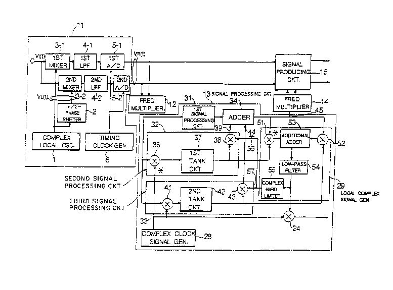
Turning to Fig. 5, the description will be
directed to a demodulator circuit according to a
preferred embodiment of this invention. The demodulator
circuit comprises similar parts designated by like
reference numerals.
In Fig. 5, the signal processing circuit 13
comprises a complex clock signal generator 28 and a local
complex signal producing circuit 29. The complex clock
signal generator 28 is for generating a complex clock
signal representing a first complex number and having a
frequency which is substantially equal to the particular
frequency. The complex clock signal is represented as
follows:
V28(t) = ej( KL KL) (13)
In the manner which will later be described in detail,
the local complex signal producing circuit 29 is for
12 207 8636
producing a complex local signal representing a second
complex number. It is assumed that the complex local
signal is represented as follows:
V29(t) = ei~(t). (14)
The signal processing circuit 13 further
comprises first, second, and third signal processing
circuits 31, 32, and 33 and an adder 34 each of which
will be described in the following.
The first signal processing circuit 31 is
connected to the frequency multiplier 12 and is for
processing the multiplied signal into a first processed
signal represented as follows:
V31(t) = a(t)ei (m~Rt+m~R-arctan m~R~) (15)
The second signal processing circuit 32 is
connected to the frequency multiplier 12, the complex
clock signal generator 28, and the local complex signal
producing circuit 29 and is for processing the multiplied
signal into a second processed signal in accordance with
the complex local signal and a conjugate complex clock
signal which represents a complex conjugate of the first
complex number. It is readily possible to make the
complex clock signal generator 28 generate the complex
clock signal as well as the conjugate complex clock
signal. The second processed signal will become clear
from the following description.
The second signal processing circuit 32 comprises
a first multiplier 36, a first tank circuit 37, and a
second multiplier 38. The first multiplier 36 is
13 2078636
connected to the frequency multiplier 12 and the complex
clock signal generator 28 and is for multiplying the
multiplied signal by the conjugate complex clock signal
to produce a first product signal which is represented as
follows:
V36(t) = VR (t) V28 (
= (b(t)ei( Ke Ke) + a(t)e i( KL KL)
(t)e~i((~K+~KL)t+~K+~L))ej R R ,
(16)
where Ke K KL
and ~Ke K KL-
The first tank circuit 37 is connected to thefirst multiplier 36 and is for processing the first
product signal into a first filtered signal which is
represented as follows:
V37(t) = b(t)ei((m~R+~Ke)t+m~R+~Ke-arctan(m~R+~K )I)
(17)
The second multiplier 38 is connected to the
local complex signal producing and the first tank
circuits 29 and 37 and is for multiplying the complex
local signal by the first filtered signal to produce a
second product signal which is represented as follows:
V38(t)
= V37(t)~V29 (t)
= b(t)ei((m~R+~Ke)t+m~R+~Ke-arctan(m~R+~Ke)T-~(t))
(18)
The second product signal is supplied as the second
processed signal to the adder 34 through a line 39 which
14 2078636
may be referred to as a first local supply arrangement.
The third signal processing circuit 33 is
connected to the frequency multiplier 12, the complex
clock signal generator 28, and the local complex signal
producing circuit 29 and is for processing the multiplied
signal into a third processed signal in accordance with
the complex clock signal and a conjugate complex local
signal which represents a complex conjugate of the second
complex number. The third processed signal will be clear
from the following description.
The third signal processing circuit 33 comprises
a third multiplier 41, a second tank circuit 42, and a
fourth multiplier 43. The third multiplier 41 is
connected to the frequency multiplier 12 and the complex
clock signal generator 28 and is for multiplying the
multiplied signal by the complex clock signal to produce
a third product signal which is represented as follows:
V41(t) = VR (t) VKL( )
= (c(t)e i( Ke Ke) + a(t)ej( LK KL)
b(t)ei((~K+~KL)t+~K+HKL))ej R R .
(19)
The second tank circuit 42 is connected to the
third multiplier 41 and is for processing the third
product signal into a second filtered signal which is
represented as follows:
V42(t) = C(t)ei((m~R ~Ke)t+m~R-HKe-arctan(m~R-~K )I)
(20)
2 0 7 8 6 3 6
The fourth multiplier 43 is connected to the
local complex signal producing and the fourth tank
circuits 29 and 42 and is for multiplying the conjugate
complex local signal by the second filtered signal to
produce a fourth product signal which is represented as
follows:
V43(t) = V42(t)'V29(t)
= C(t)ei((m~R ~Ke)t+m~R-~Ke-arctan(m~R-~Ke)~+~(t))
(21)
The fourth product signal is supplied as the third
processed signal to the adder 34 through a line 44 which
may be referred to as a second local supply arrangement.
The adder 34 is for summing up the first, the
second, and the third processed signals into a sum signal
which is represented as follows:
V34(t) = ei( ~R R)
X (a(t)e~jarctan m4)R~
+ b(t)ei (h)Ket+~Ke-arctan(m4JR+~)Ke)T-~D(t) )
+ C(t)ei(~~Ket~~Ke~arctan(m~R~~Ke)~+~(t)))
(22)
The sum signal is supplied as the modified signal to the
demultiplier 14 through a line 45 which may be referred
to as a supply arrangement.
The description will be directed to the local
complex signal producing circuit 29. The local complex
signal producing circuit 29 comprises a first correlation
detector 51, a second correlation detector 52, an
additional adder 53, a low-pass filter 54, and a complex
lÇ 2078636
hard limiter 55, each of which will be described in the
following. It is to be noted herein that the sum signal
represents a particular complex number, the first
processed local signal representing a first specific
complex number, the first filtered signal representing a
second specific complex number.
The first correlation detector 51 is connected to
the afore-mentioned adder 34 and the first tank circuit
37 and is for multiplying the sum signal supplied from
the adder 34 by a conjugate first filtered signal
supplied from the first tank circuit to produce a first
correlation signal. The conjugate first filtered signal
represents a compléx conjugate of the first filtered
signal. The first correlation signal is represented as
follows:
V51tt)
= V37(t)~V34*(t)
= b(t)(a(t)ei(~Ket+~Ke-arctan(m~R+~Ke)r+arctan m~R~)
+ b(t)eiS~(t)
+ C(t)ei(2~Ket+2~Ke+arctan(m~ -~Ke)~-arctan(m~R+~Ke)~-~(t))
~ (23)
The second correlation detector 52 is connected
to the adder 34 and the second tank circuit 42 and is for
multiplying a conjugate sum signal supplied from the
adder 34 by the second filtered signal supplied from the
second tank circuit 42 to produce a second correlation
17 2078636
signal. The conjugate sum signal represents a complex
conjugate of the sum signal. The second correlation
signal is represented as follows:
V52(t)
= V42(t)-V34(t)
= C(t)(a(t)ei(~Ket+~Ke+arctan(m~R-~Ke)~-arctan m~R~)
+ b(t)ej(2~Ket+2~Ke+arctan(m~R-~Ke)l-arctan(m~R+~Ke)~
+ c(t)ej~(t)) (24)
The additional adder 53 is connected to the first
and the second correlation detectors 51 and 52 and is for
summing up the first and the second correlation signals
into an additional sum signal which is represented as
follows:
V53(t)
(b2 + c2)ej~(t)
+ aej( Ke ~Ke)(bej(arCtan(m~R+~Ke)l-arctan m~RT)
+ cej(arctan(m~R-~Ke)~-arctan m~RI))
+ 2bce Ke Ke),ej(arctan(m~R-~Ke)r-arctan(m~ +~ )l-~)
(25)
In order to maintain a normal condition of the
additional adder 53, it is necessary that ~(t) has a
frequency equal to ~Ke.
Herein, it will be assumed that:
ei~(t) = ei(~Ket+0Ke+~) (26)
where ~ represents the phase error. In this event, the
additional sum signal is represented as follows:
V53,(t) = ej(~Ket+~Ke+~m(t)), (27)
where:
18 2078636
e j~om(t)
= (b + c2)ei~ + abe~i(arctan(m~R+~Ke)~-arctan m~R~)
+ acei(arctan(m~R-~Ke)~-arctan m~R~)
+ 2bce-j~ej(arctan(m~R-~Ke)~-arctan(m~R+~Ke)~)
(28)
The low-pass filter 54 is connected to the
additional adder 53 and is for carrying out an averaging
operation of the additional sum signal to produce an
averaged signal having an amplitude representative of a
result of the averaging operation. The averaged signal
is represented as follows:
V54(t) = ei(~Ket+~Ke+~m(t)-arctan ~K D) (29)
where D represents a time constant, D ~ 7.
In Equation (29), ~Ke is very small.
Accordingly, Equation (28) is rewritten into:
ei~m(t) '_ (b2 + c2)ei~ + a(b + c) + 2bce i~. (30)
In this event, the averaged signal is represented as
follows:
ei~m = (b2 + c2)ei0 + a(b + c) + 2bce i0, (31)
where each of a, b, and c represents the amplitude of the
averaged signal and is represented by an integer.
Furthermore, ei~ represents a phase component of the
averaged signal, where ~ < 1.
The complex hard limiter 55 is connected to the
low-pass filter 54 and is for limiting the amplitude of
the averaged signal to produce a limited signal. Since
the limited signal represents the phase component of the
averaged signal, the following equation is introduced.
19 2078636
d~ - arctan ~KeD = ~. (32)
Therefore:
~ = -arctan ~KeD/(l ~ d). (33)
Thus, the phase error ~ is maintained in a predetermined
range. Generally, the phase error ~ becomes as follows:
~ ~ 0. (34)
More particularly, the limited signal represents
a second complex number and may therefore be called
herein the complex local signal. In addition, the
complex hard limiter 55 carries out a predetermined
calculation in accordance with the complex local signal
to produce the conjugate complex local signal as a result
of the predetermined calculation in the manner known in
the art.
The complex local signal is supplied to the
second multiplier 38 through a line 56 which will be
referred to as a first additional supply arrangement.
The conjugate complex local signal is supplied to the
fourth multiplier 43 through a line 57 which will be
referred to as a second additional supply arrangement.
The signal processing circuit 13 further
comprises an additional multiplier 58 connected to the
complex clock signal generator 28 and the low-pass filter
54. The additional multiplier 58 is for multiplying the
complex clock signal by the averaged signal to produce a
particular clock signal which represents the
above-mentioned clock component.
2078636
The description will be turned back to the adder
34. Equation (22) is rewritten into:
V34,(t) = ei(m Rt R)
X ( ae~i arctan m~R~ + be~i ( arctan ( m~R+~Ke ) +0 )
+ ce~ arCtan(m~R~~Ke))). (35)
When ~Ke is sufficiently small, Equation (35) is
rewritten into:
V16(t) ~ (a + b + c)ei(m~Rt+m~R-arctan(m~R~)) (36)
When the above-mentioned m is constant, a represents
nonzero. The m is increased, b represents nonzero. The
m is decreased, c represents nonzero. Accordingly, (a +
b + c) is not equal to zero. As a result, the DC
component is obtained regardless of the value of m.
As is clear from Equation (31), the clock
component is present in a stable form in a case where
both of b and c are not zero, namely, where the modulated
signal has a change point therein. Accordingly, the DC
component is produced by using the stable form of the
clock component even when the clock component is present.
While the present invention has thus far been
described in connection with only a single embodiment
thereof, it will readily be possible for those skilled in
the art to put this invention into practice in various
other manners. For example, each of the first signal
processing, the first tank, and the second tank circuits
31, 37, and 42 may be a low-pass filter in the manner
known in the art.