Note: Descriptions are shown in the official language in which they were submitted.
1 2078705 NE-459
TITLE OF THE INVENTION
Method and arrangement of coherently demodulating
PSK signals using a feedback loop including a filter bank
BACKGROUND OF THE INVENTION
5Field of the Invention
The present invention relates to a method and
arrangement of coherently demodulating PSK (Phase Shift
Keying) signals, and more specifically to such a method
and arrangement via which an incoming multi-phase phase-
modulated signal can effectively be reproduced`
irrespective of a large amount of carrier frequency
deviations and via which proper operations can be assured
under low C/N (carrier to noise ratio) environments. The
present invention is well suited for use in a mobile
communications system by way of example.
Description of the Prior Art
As is known in the art, coherent (viz., synchronous)
demodulation is to detect baseband signals through
multiplication of incoming modulated IF (Intermediate
Frequency) signals by a reproduced carrier signal.
Before turning to the present invention it is deemed
preferable to discuss a prior art technique with
reference to Figs. 1 and 2. Fig. 1 is a block diagram
showing a conventional coherent demodulator which is
generally depicted by reference numeral 10. Fig. 2 is a
block diagram illustrating in detail a single-tuned
filter of Fig. 1.
In Fig. 1, a m-phase phase-modulated analog IF
signal Vin is applied to two mixers 12, 14 (m is a
positive integer such as 2, 4, 8, 16, ..... ). The
incoming signal Vin is given by
Vin = p cos(Wct+~c) - q sin(Wct+~c)
= 1/2{(p+jq)e~ (WCt~C)
+ (p jq)e~~(Wct~c) ....... (1)
where p, q indicate respectively modulating signals, Wc
~ - 2 - 2078705 NE-459
an angular frequency of a carrier signal, and e~ (Wct+5c) the
carrier signal.
The mixer 12 is coupled to a local oscillator 16
while the other mixer 14 is coupled, via a ~/2 phase
shifter 18, to the oscillator 16. A local signal Vo
generated from the blocks 16, 18 is given by
Vo = e~ (Wot+30)
= cos(Wot+~o) + jsin(Wot+~o) ... (2)
In more specific terms, if the output of the local
oscillator 16 is cos(Wot+~o) then the output of the phase
shifter 18 is sin(Wot+~o) or vice versa. The output of
the mixers 12, 14 (denoted by Vmix) is written by
Vmix = Vin Vo* = (p+jq)e~ (Wrt+ar)
+ [components of (Wo+Wc)] (3)
where * indicates a conjugate complex number, and
Wr = Wc - Wo
~r = ~c - ~o
Low-pass filters (LPFs) 20, 22 are provided to remove the
~con~ term of the right side of equation (3). Thus,
analog-to-digital (A/D) converters 24, 26 produce the
following signal Vad.
Vad = (p+jq)e~ (Wrt+~r)
A timing circuit 28 is provided to apply timing
clocks (CLKs) to a plurality of digital blocks which
follow the low-pass filters 20, 22. The application of
timing clocks to digital blocks, however, is not shown
merely for the sake of simplifying drawings.
The output Vad of the A/D converters 24, 26 is
applied, via ch~nnel filters (viz., matched filters) 30
and 32, to delay circuits 34, 36 and also to a multiplier
(viz., power-of-m circuit) 38.
The multiplier 38 multiplies the output Vad by
itself m times and generates a signal denoted by Vad.
Vadm = (p+iq)~e~Dl(wrt+~r)
= e~(wrt+9r) + [noise components] -- (5)
2078705
- 3 - NE-459
The multiplier 38 applies the output thereof to a
single-tuned filter 40 which, as shown in Fig. 2,
includes an adder 42, a constant value generator 44, a
multiplier 46 and a delay circuit 48. The constant value
generator 44 issues a real value denoted by a, while the
delay circuit 48 retards the output of the adder 42 by
one sampling time period.
The transfer function of the filter 40 is written by
T(Z) = 1/(1 - az~1) ... (6)
where Z = eST (S is a differential operator, and T a
sampling period).
If the sampling frequency is sufficiently high,
equation (6) can be approximated as follows.
T(S) = {1/(1-a)}/(l+SI) ... (7)
where I = aT/(1-a)
Thus, the output of the filter 40, denoted by Vt, is
given by
Vt = {1/~ 1+(Wrl) 2} e~ (m(Wrtl ~r)-t~ mWr~}
+ [noise components] ... (8)
Accordingly, the frequency error Wr causes the following
problems.
(a) The amplitude of Vt is lowered and thus C/N is
reduced; and
(b) Phase drift represented by tan~1mWrl is
undesirably i-nduced.
Merely for the convenience of simplifying the
discussion, it is assumed that the value of ar is
sufficiently small.
A divider 50 divides the received signal by itself m
times and, generates the output (denoted by Vrc) which is
a reproduced carrier and written by
Vrc = Vt1/m = e~l(wrt,~r)-t~wrT~
Following this, the reproduced carrier Vrc is multiplied
by Vad at the multiplier 52 (Fig. 1). Thus, the
modulating signals p, q are reproduced at the output of
- 4 - 2078705 NE-459
the multiplier 52. The output of the multiplier 52
(denoted by Vdm) is given by
Vdm = Vad Vrc~
= (p~jq)e~ t~ WrT
= (p~jq)e ............................ - (9)
It is understood that in order to accurately reproduce
the modulating signals p and q, the frequency difference
Wrl should be rendered zero.
As mentioned above, merely one filter (viz., filter
10~ 40) is provided in the conventional coherent demodulator
10 and, accordingly it is extremely difficult to properly
determine or design the pass-band of the filter 40. That
is, if the pass-band of the filter 40 is narrowed to
increase a signal-to-noise ratio (S/N) for complying with
low C/N environments, it may fail to transfer the
received signal therethrough if the frequency difference
Wr~ exhibits a large amount of value. Conversely, if the
pass-band is ext~-n~e~ or widened, another problem is
caused which undesirably lowers S/N. Further, if a large
amount of frequency deviation occurs in the carrier, the
prior art may be unable to implement the coherent
detection using such a single filter.
SUMMARY OF THE INVENTION
It is an ob;ect of the present invention to provide
a method which eliminates or effectively reduces the
above mentioned prior art problems.
Another ob;ect of the present invention is to
provide a hardware arrangement which eliminates or
effectively reduces the above mentioned prior art
problems.
Still another object of the present invention is to
provide a method wherein a feedback loop including a
plurality of filters is provided to effectively replicate
a carrier irrespective of the frequency deviation thereof
exhibits a large value.
2078705
Still another object of the present invention is to
provide a hardware arrangement wherein a feedback loop
including a plurality of filters is provided to
effectively reproduce a carrier irrespective of the
frequency deviation thereof exhibits a large value.
These objects are fulfilled by a technique wherein
in order to coherently demodulate an incoming multi-phase
PSK analog signal irrespective of large frequency
deviation, an automatic frequency feedback loop is
provided. An analog baseband signal is generated by
multiplying the IF analog signal by a local signal and
then is converted into the correspon~ing digital baseband
signal. A multiplier multiplies the digital baseband
signal by another local signal. The output of the
multiplier is further multiplied and then applied to a
plurality of single-tuned filters which are arranged in
parallel and have tuning frequencies each different from
an adjacent frequency by a predetermined frequency
interval. Each of the plurality of single-tuned filters
generates a signal for use in carrier recovery, a
frequency error signal and a correlation coefficient.
Subsequently, one of the plurality of single-tuned
filters is selected in a manner wherein the maximum value
is detected among the correlation coefficients. The
another local signal is generated using the frequency
error signal of the single-tuned filter which has been
selected. A modulating signal is reproduced using the
recovered carrier in a conventional manner.
A first ob;ect of the present invention comes in a
method of coherently detecting a multi-phase PSK IF
analog signal, comprising the steps of: (a) generating an
analog baseband signal by multiplying the multi-phase PSK
IF analog signal by a first local signal; (b) converting
the analog baseband signal into the corresponding digital
baseband signal, (c) generating a first signal by
- 6 - 2078705 NE-459
multiplying the digital baseband signal by a ceco~ local
signal; (d) generating a seco~ signal by multiplying the
first signal predetermined times; (e) applying the second
signal to a plurality of single-tuned filters which are
arranged in parallel and have tuning frequencies each
different from an adjacent frequency by a predetermined
frequency interval, each of the plurality of single-tuned
filters generating a third signal, a frequency error
signal and a correlation coefficient between input and
output thereof; (f) selecting one of the plurality of
single-tuned filters by detecting the maximum value among
the correlation coefficients; (g) generating the second
local signal using the frequency error signal of the
single-tuned filter which has been selected in step (f);
(h) generating a reproduced carrier by dividing the third
signal the predetermined times; and (i) reproducing a
modulating signal by multiplying the first signal by the
reproduced carrier.
A second aspect of the present invention comes in an
arrangement of coherently detecting a multi-phase PSK IF
analog signal, comprising: first means for generating an
analog baseband signal by multiplying the multi-phase PSK
IF analog signal by a first local signal; second means
which is coupled to the first means and converts the
analog baseband signal into the corresponding digital
baseband signal; third means which is coupled to the
seConA means and generates a first signal by multiplying
the digital baseband signal by a second local signal;
fourth means for generating a second signal by
multiplying the first signal predetermined times; fifth
means for applying the cecon~ signal to a plurality of
single-tuned filters which are arranged in parallel and
have tuning frequencies each different from an adjacent
frequency by a predetermined frequency interval, each of
the plurality of single-tuned filters generating a third
~ 7 2078705 NE-459
signal, a frequency error signal and a correlation
coefficient between input and output thereof; sixth means
for selecting one of the plurality of single-tuned
filters by detecting the maximum value among the
correlation coefficients; seventh means for generating
the second local signal using the frequency error signal
of the single-tuned filter which has been selected by the
sixth means; eighth means for generating a reproduced
carrier by dividing the third signal the predetermined
times; and ninth means for reproducing a modulating
signal by multiplying the first signal by the reproduced
carrier.
BRIEF DESCRIPTION OF THE DRAWINGS
The features and advantages of the present invention
will become more clearly appreciated from the following
description taken in con;unction with the accompanying
drawings in which like elements are denoted by like
reference numerals and in which:
Fig. 1 is a block diagram showing the prior art
arrangement discussed in the opening paragraphs of the
instant disclosure;
Fig. 2 is a block diagram showing a filter which
forms part of the Fig. 1 arrangement;
Fig. 3 is a block diagram showing an embodiment of
the present invention;
Fig. 4 is a block diagram showing one of a plurality
of filters which form part of the Fig. 3 arrangement;
Fig. 5 is a diagram showing a plurality of tuning
frequencies of the filters in relation to filter gains
thereof;
Fig. 6 is a diagram showing numerical values which
are respectively indicated by frequency error signals
generated from the filter bank of Fig. 3; and
Fig. 7 is a diagram showing numerical values which
are derived by shifting the values shown in Fig. 6.
- 8 ~ 207 87 05 NE-459
DETAILED DESCRIPTION OF THE
PREFERRED EMBODIMENTS
An embodiment of the present invention will be
discussed with reference to Figs. 3 to 7.
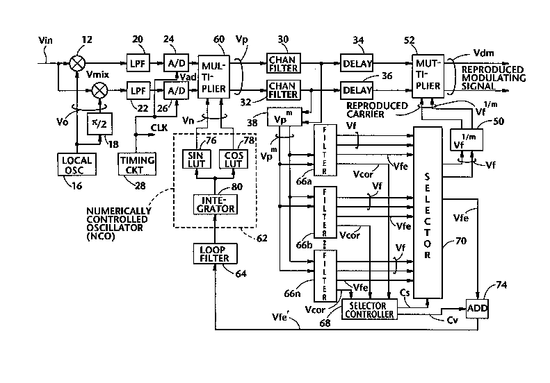
In brief, the arrangement of Fig. 3 differs from
that of Fig. 2 in that the former arrangement further
includes, a first multiplier 60, a numerically
controlled oscillator (NCO) 62, a loop filter 64, a
plurality of filters 66a-66n, a selector controller 68, a
selector 70 and an adder 74. As shown, the NCO 62
includes a SINE look-up table (LUT) 76, a COSINE look-up
table (LUT) 78 and an integrator 80.
The filters 66a-66n are configured in the same
manner with one another and takes the form of a single-
tuned type. The frequency interval between the tuning
frequencies of the adjacent filters is ~W.
Fig. 4 is a block diagram showing in detail one of
the filter bank (viz., filters 66a-66n) which includes an
adder 80, a constant value generator 82 which issues a
complex value (viz., e~ where W is an angular frequency
and T a sampling time period), a multiplier 84, a delay
circuit 86, a correlator 88 and two low-pass filters 90,
92.
Merely for the convenience of discussion, the tuning
frequencies of the filters 66a-66n are denoted by k~W (k
= O, +l, +2, ...) as illustrated in Fig. 5. Thus, the
transfer function T(Z:k) of the filter which has the
tuning frequency k~W, can be represented by
T(Z;k) = 1/{1-ae~ Z~~) ... (10)
Z has been defined in connection with equation (6).
Equation (10) is rewritten by
T(W;k) = T(W-k~W;O) ... (11)
It is assumed that the output of the NCO 62 (denoted
by Vn) is represented by
Vn = e~(wn~n) ... (12)
9 - ~ 2078~05 NE-459
Thus, the multiplier 60 generates the output thereof
(denoted by Vp) which is given by
Vp = Vad Vn*
= (p+jq)e~(wpt+~p) ... (13)
where Wp = Wad - Wn
~p = ~ad - ~n
The value Wp indicates a frequency deviation of the
carrier.
The output of the multiplier (viz., power-of-m
circuit) 38 is given by
Vpm = (p+jq)me.lm(wPtl~p)
= ejm(Wpt+~p) + [noise components] ... (14)
The output Vpm is applied to the filters 66a-66n.
As mentioned above, it is assumed that the filter
shown in Fig. 4 is a filter which has the tuning
frequency k~W. The output Vpm is applied to the adder 80
and the correlator 88. The delay circuit 86 retards the
output of the adder 80 by one sampling time period. The
transfer function of the filter is given by equation 10
and hence the output of the adder 80 (viz., the output of
the filter shown in Fig. 4) can be written by
Vf = {1/~ l+(mWp-k~W)2lZ}
x e~(Wpt~p)-t~l(mwp-~w)~ (15)
Deriving equation (15) is known to those skilled in the
art and does not important to an underst~n~ ng of the
present invention, and thus will be omitted for brevity.
On the other hand, the output of the correlator 88
is given by the following equation.
Vpm-Vf* = {1/~1 l+(mWp-k~W)2l2}
X e~tan (mWp-k~w)~
= l/Cl+(mWp-k~W)2}
+ j{(mWp-k~W)/(l+(mWp-k~W)2)}... (16)
The real part of equation (16) indicates a correlation
coefficient and is applied, via the LPF 92, to the
selector controller 68 as Vcor. On the other hand, the
lO - 20787 05 NE-459
imaginary part of equation (27) indicates a tuning
frequency error value and is applied, via the LPF 90, to
the selector 70 as Vfe.
The selector controller 68 determines which is the
highest value among the correlation coefficients applied
thereto from the filters 66a-66n. It is assumed that the
filter 66b has the tuning frequency ~W and issues the
highest correlation coefficient. In such a case, the
controller 68 produces a control signal Cs which
indicates the filter 66b. The selector 70 selects the
filter 66b in response to the control signal Cs, and thus
acquires the complex signal Vf and the frequency error
signal Vfe both from the filter 66b. The signal Vf is
relayed to the divider 50, while the frequency error
signal Vfe to the adder 74. The demodulated signal Vdm
derived from the multiplier 52 is given by
Vdm = (p+jq)e~r ... (17)
The frequency deviation Wp of equation (17) should
be rendered zero in order to exactly reproduce the
modulating signals p and q. This is implemented using
the feedback path which includes the adder 74, the loop
filter 64 and the NC0 62.
Fig. 6 is a diagram which shows a plurality of
characteristic curves which respectively indicate
numerical values of the error signals Vfe outputted from
the selector 70. In fig. 6, the tuning frequencies of
the filters 66a, 66b, 66c, 66d, 66e, ...., 66n are
respectively denoted 0, +~W, -~W, +2~W, -2~W, +3~W, -3~W,
..... ..., +n~W and -n~W (for example).
It is assumed that the selector controller 68
selects the filter 66b. In this instance, the controller
68 supplies the adder 74 with a control signal Cv which
indicates a predetermined constant (depicted by L).
Thus, the characteristic curve with the tuning frequency
~W is shifted by L as shown in Fig. 7. Similarly, if
Il - 2078705 NE-459
the selector 68 selects the filter 66d, the selector
controller 68 supplies the adder 74 with a constant
signal Cv indicative of a constant value 2L.
Accordingly, the curve with the tuning frequency 2~W is
shifted by 2L as illustrated.
The output of the adder 74 is applied, via the loop
filter 64, to the integrator 80 of the NCO 62. The
integrator 80 is a digital differential analyzer which
accumulates the numerical values applied from the adder
74 using the timing clocks (CLKs). The integrated values
are sllccpc~ively applied to the SINE and COSINE look-up
tables 76, 78 which in turn generate the signal Vn (see
equation (12). Following this, Vn is multiplied by the
complex signal Vad as mentioned above. Thus, the
frequency deviation Wp in the output of the multiplier 60
gradually appro~che~ zero and ultimately converges to
zero.
According to the present invention, even if the
frequency deviation Wp exhibit a large value such that
the prior art filter is unable to tune to the signal
àpplied thereto, the filter bank of the present invention
is able to sllccec~fully tune to the received signal using
one of the filters 66a-66n. Thus, the frequency
deviation Wp is eventually rendered zero.
It will be understood that the above disclosure is
representative of one possible embodiment of the present
invention and its variant and that the concept on which
the invention is based is not specifically limited
thereto.