Note: Descriptions are shown in the official language in which they were submitted.
2078'31
- 1 -
POSITIONAL DEVIATION MEASURING DEVICE AND METHOD THEREOF
BACKGROUND OF THE INVENTION
Field of the Invention
The present invention relates to a positional
deviation measuring device and a method thereof which are
suitable for use as the positional deviation measuring
device and method for measuring the positional deviation
between superimposed patterns when fine electronic circuit
patterns formed on objects (hereinafter referred to as
reticles), such as a plurality of masks or reticles, are
aligned with and printed on a second object, such as a
wafer, by an exposure apparatus. used for manufacturing
semiconductor devices.
Description of the Related Art
In a semiconductor-manufacauring exposure apparatus
for transferring circuit patterns on reticles onto the
photo-sensitive member of a wafer using ultraviolet
radiation or X-rays, relative positioning between the
reticle and the wafer is an essential factor for increasing
the performance of the apparatus. The positioning
operation conducted by the currently used exposure
207873I
_ 2 _
apparatus requires a positioning accuracy of the order of,
for example, a submicron or less, to achieve a high degree
of integration of the semiconductor devices.
In many positioning device s, a so-called alignment
pattern is provided on the ret:icle and on the wafer for
positioning, and alignment between the reticle and the
wafer is performed by utilizing the positional data
obtained from the alignment patterns. The positioning
performance of an exposure apparatus is conventionally
measured and evaluated by prini:ing the fine pattern formed
on the reticle onto the wafer and then by visually
measuring or measuring through an image processing
operation the deviation between the pattern printed on the
wafer and a pattern previously formed on the wafer.
However, the visual measuring method has drawbacks in
that (1) the measurement accur<icy thereof largely depends
on the experience or skill of l.he operator and is. thus
unstable, (2) it requires time and is inconvenient because
it is manually done, and (3) the measurement accuracy is
low.
The measurement method based upon an image processing
operation suffers from problems in that the technique
thereof is complicated and requires a great deal of time,
and in that a high measurement accuracy cannot be obtained.
2~'~873~
- 3 -
It is an object of the present invention to overcome
the deficiencies of the prior a.rt.
It is another object of the present invention to
provide a positional deviation measuring device which can
automatically measure the posit.ional deviation between
superimposed patterns on an object.
It is still another object of the present invention to
provide a positional deviation measuring device in which
the measuring time for measuring the positional deviation
between superimposed patterns i.s reduced.
It is still another object of the present invention to
provide a positional deviation measuring device which
assures high accuracy measurements of the positional
deviation between superimposed patterns.
According to one aspect, the present invention which
achieves at least one of these objectives relates.to a
device for measuring the positional deviation between a
plurality of diffraction gratings formed on the same
object, the device comprising an illumination optical
system for illuminating the plurality of diffraction
gratings with a light beam, the illumination by said
illumination optical system generating a plurality of
diffracted light beams from the plurality of diffraction
gratings, an interference optical system for forming at
2078'31
- 4 -
least one interference light be=am from the plurality of
diffracted light beams, a dete<aor for detecting the at
least one interference light beam, wherein the result of
the detecting by the detection serves as the basis for
measuring the positional deviation between the plurality of
diffraction gratings, and a measuring system for measuring
the relative positional relation between the illumination
optical system and the plurality of diffraction gratings.
The plurality of diffraction gratings can be two
equidistant linear diffraction gratings. Also, the
interference optical system can form two separate
interference light beams from t:he diffracted light beams
respectively generated from the' two diffraction gratings.
In addition, the measuring system comprises imaging means
for imaging the plurality of diffraction gratings through
the interference optical system.
The device can further comprise a light-receiving
element for receiving a diffracaed light beam which is
generated from the at least one: of the plurality of
diffraction gratings by the illumination of the
illumination optical system and which is not incident on
the interference optical system, and means for measuring
the relative positional relatic>n between the interference
optical system and the plurality of diffraction gratings
from a position on the light-receiving element at which the
- 5 - -
diffracted light beam, which i:c not incident on the
interference optical system, i:; incident. Also, the
measuring system measures the rotational positional
deviation about a direction perpendicular to the surface on
which the object on which the ~rlurality of diffraction
gratings are formed.
According to another aspects, the present invention _
which achieves at least one of these objectives relates to
a method of measuring the posit.ional deviation between a
plurality of diffraction gratings formed on the same
object, the method comprising the steps of illuminating the
plurality of diffraction gratings with a light beam from an
illumination optical system, th.e illumination generating a
plurality of diffracted light beams from the plurality of
diffraction gratings, forming a.t least one interference
light beam from the plurality of diffracted light beams
using an interference optical system, detecting at least
one interference light beam, and using the result of the
detec~Eing to measure the positional deviation between the
plurality of diffraction gratings, measuring the relative
positional relation between the illumination optical system
and the plurality of diffraction gratings, and aligning the
illumination optical system with the object on the basis of
the results of the measuring step, the illumination in the
illuminating step being performed on the plurality of
207731
- 6 -
diffraction gratings which have been aligned in the
alignment step.
The plurality of -diffract.ion gratings can be two
equidistant linear diffraction gratings. Also, the method
can further comprise the step of forming separate
interference light beams from ithe diffracted light beams
respectively generated from the two diffraction gratings
with the interference optical System. In addition, the
measuring step comprises the si.ep of using imaging means
for imaging the plurality of d:Lffraction gratings through
the interference optical system.
The measuring step can further comprise the steps of
receiving a diffracted light beam, which is generated from
the at least one of the plurality of diffraction gratings
by the illumination of the illumination optical system and
which is not incident on the interference optical system,
with a light receiving element, and measuring the. relative
positional relation between the' interference optical system
and the plurality of diffraction gratings from a position
on the light-receiving element at which the diffracted
light beam, which is not incident on the interference
optical system, is incident. The measuring step can also
comprise the step of measuring the rotational positional
deviation about a direction perpendicular to the surface of
the object on which the plurality of diffraction gratings
~fl~'8~~~1
are formed.
Other and further objects will be apparent from the
following description of embodiments with reference to the
accompanying drawings.
Fig. 1 illustrates the principle of the present
invention;
Fig. 2 illustrates how a 7Light beam is incident on a
diffraction grating;
Fig. 3 illustrates a phase' shift between a reference
signal and a signal to be measured;
Fig. 4 illustrates a schematic view of the structure
of a measuring device;
Fig. 5 is a plan view of ciiffraction gratings on a
wafer;
Fig. 6 is a front view of an edge mirror;
Fig. 7 is a perspective view of a rotational
interference optical system;
Fig. 8 is a side elevation view of a rotational
interference optical system;
Fig. 9 illustrates a schematic view of the structure
of the essential parts of a first embodiment according to
the present invention;
Fig. 10 illustrates a schematic view of the overall
structure of the first embodiment;
Fig. 11 illustrates the images of diffraction gratings
on a TV screen;
Figs. 12(a) and 12(b) illustrate the intensity
distribution of a TV scanning 7_ine;
Fig. 13 illustrates a schematic view of the case in
which a prism is shifted;
Fig. 14 illustrates a schematic view of the case in
which a plane glass is used;
Fig. 15 illustrates a schematic view of another
embodiment of the present invention; and
Fig. 16 is a perspective view of a photodetector and a
signal processing system.
DETAIT ED DESGRIPTr_ON ~F TFiE PREFERRED EMBODIMENTS
A positional deviation measuring device according to
the embodiments described below includes an illumination
optical system for illuminating first and second grating
patterns formed on an object with coherent light, an
interference optical system for causing the diffracted
light emanating from the first and second grating patterns
to interfere with each other, a detecting portion for
detecting the relative positional deviation between the
first and second grating patterns by obtaining the phase
difference between the interference light beams generated
20~8~~1
- 9 -
v
by the interference optical sy:~tem, and a measuring portion
for measuring the deviation between the illumination
optical system and the first and second grating patterns.
In the positional deviation measuring device having
the aforementioned structure, t:he first and second grating
patterns are illuminated with coherent light, and the
diffracted light beams emanating from the first and second
grating patterns are caused to interfere with each other to
detect the relative positional deviation between the first
and second grating patterns. p,lso, the deviation between
the first and second grating patterns and the illumination
optical system is measured.
The principle of measurement of the positional
deviation will be described in detail. Fig. 1 illustrates
how an equidistant linear diffraction grating 2 whose
grating lines extend in a direction perpendicular to the
surface of the page on which Fig. 1 is printed is
illuminated with laser beams L1 and L2, which are plane
waves having an angle of incidence of the same absolute
value and slightly different frequencies. Where m is the
number of the order of the diffracted light, a diffracted
light of the +mth order is the diffracted light located to
the left of the direction of propagation of the diffracted
light of the zeroth order, and a diffracted light of the -
mth order is the diffracted light located to the right of
207831
- 10 ~~
the direction of propagation oi° the diffracted light of the
zeroth order. The diffracted light of - first order
produced from the light beam L~'~. by the diffraction grating
2 is directed perpendicular to the surface of the wafer 1.
It is a known fact that when the diffraction grating 2
moves by distance equal to the pitch of the diffraction
grating 2 in the x direction, t:he phase of the wave fronts
of the diffracted light beams L3 and L4 produced from the
light beams L1 and L2 by the diffraction grating 2 having a
pitch p varies by 2n, i.e., by the single wavelength. That
is, when the diffraction grating 2 shifts in the x
direction by X0, a phase change: of t2mnX0/p occurs in the
diffracted light.
A method of measuring the deviation between the
printed patterns using the above-described principle will
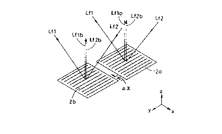
be described below. As shown i.n Fig. 2, we consider two
equidistant linear diffraction gratings (gratings) 2a and
2b located adjacent to each other in the same plane. The
two diffraction gratings 2a and 2b have the same pitch p.
There is a deviation (0x = Xb -~ Xa) in the x direction
between the diffraction gratings 2a and 2b. Xa and Xb are
respectively deviations of the diffraction gratings 2a and
2b in the x direction from the same reference position.
The complex amplitudes Uf1 and Uf2 of the two light
beams Lfl and Lf2 having slightly different frequencies
-. 2 0 7 8'~ 31
- 11 -
(t~fl, (~f2) and initial phases ~~fl and ~f2 are given by the
following equations (1) and (2), respectively.
Uf1 = AO exp {i ((~flt + ~f1) } ~ ~ ~ (1)
Uf2 = BO exp {i (C~f2t + ~f2) } ~ ~ ~ (2)
TAO and BO are constants which can be easily
determined experimentally.
the entire surface of the two diffraction gratings 2a
and 2b is illuminated with the two light beams Lfl and Lf2.
The light beams Lfl and Lf2 are projected from, for
example, the left and right sides at angles of incidence of
the same absolute value, respectively. Diffracted light
beams of + first order produced from the light beam Lfl by
the diffraction gratings 2a and 2b are indicated by Lafl
and Lbfl, respectively. Diffracted light beams of - first
order produced from the light beam Lf2 by the diffraction
gratings 2a and 2b are indicated by Laf2 and Lbf2,
respectively. Complex amplitudes Uafl(+1), Uaf2(-1),
Ubfl(+1) and Ubf2(-1) of the diffracted light beams Lafl,
Laf2, Lbfl and Lbf2 are respectively expressed by the
following equations (3) through (6)
Uaf1 (+1) - Af1 exp (wflt + + Via) (3)
{i ~fl }
Uaf2 (-1) - Af2 exp ((af2t+ + Via) (4)
{i ~f2 }
Ubf1(+1) - Bfl exp (wflt + + fib)} (5)
{i ~fl
Ubf2 (-1) - Bf2 exp ((~f2t+ + fib) (6)
{i ~f2 }
Afl, Af2, Bf1 and Bf2 are ~~onstants which can be
20'~8'~31
- 12 -
determined experimentally.
Here, we have ~a = 2nXa/p and ~b = 2nXb/p. In these
equations, the amounts of deviation of the diffraction
gratings 2a and 2b in the x dio.ection are expressed in the
form of a phase. The intensity distributions Ua and Ub of
the interference light beams obtained by interfering the
diffracted light beams Lafl an<i Laf2 produced by the
diffraction grating 2a and the diffracted light beams Lbfl
and Lbf2 produced by the diffraction gratings 2b,
respectively, are given by the following equations (7) and
(8)
Ua = ~ U'afl (+1) + U'af2 (-1) ~ 2
- Afl2 + Af22 + 2Af1 ~ Af2 cos {2n (f2-fl) t
+ (~f2 -~ ~Ofl) - 2~a} ~ ~ ~ (7)
~ Ub = ~ U'bfl.(+1) + U'bf2 (-1) ~ 2
- Bfl2 + Bf22 + 2Bf1 ~ Bf2 cos {2n (f2-fl) t
+ (~f2 - ~Of1) - 2~b} ~ ~ ~ (8)
where Afl2 + Af22 and Bfl2 + Bf22 are a d.c. component, and
2Af1 ~ Af2 and 2Bf1 ~ Bf2 are a~n amplitude, and U'afl(+1),
U'af2(-1), U'bfl(+1), and U'bf2;(-1) are complex amplitudes
of diffracted light beams Lafl, Laf2, Lbfl and Lbf2,
respectively.
The signals indicated by equations (7) and (8) are
those having a beat frequency of f2 - fl and an initial
phase difference of ~f2 - ~f1 and which have been phase
~~78731
- 13 ~-
modulated by deviations ~a and ~b of the diffraction
gratings 2a and 2b, respective:Ly. Thus, the initial phases
of the light beams can cancel each other and a phase
difference 0~ _ ~b = ~a = (2 n/p)Ox can be detected with a
high degree of accuracy by the so-called heterodyne
interference method by using either one of the signals
expressed by equations (7) and (8) as a reference signal
while employing the other ode as a signal to be measured
and by detecting the time deviation between the two
signals.
As mentioned above, the heterodyne interference method
is a method which detects the phase difference between the
two signals over time. Therefc>re, the detection is not
affected by a difference in they d.c. components of the
signals or a change in the amplitudes thereof. If the time
difference between a reference signal gl and a signal to be
measured g2 is indicated by fit, as.shown in Fig. 3, the
phase difference between the two signals can be measured
with a high degree of accuracy by accurately detecting time
difference OT by using, for example, a lock-in amplifier.
Since the thus-detected phase difference corresponds
to the phase difference 0~ representing the deviation
between the diffraction gratings 2a and 2b, the deviation
between the diffraction gratings 2a and 2b can be obtained
from p'~~/2n. Thus, the positioning accuracy of the
207731
- 14 ~-
semiconductor device exposure apparatus, i.e., the
positional deviation between the device pattern printed in
the first exposure operation and that printed in the second
exposure apparatus, can be detected by obtaining the
deviation between the grating pattern (which may be 2a)
printed in the first exposure operation and the grating
pattern (which may be 2b) printed in the second exposure
operation on the basis of the aforementioned principle.
Fi.g. 4 illustrates the structure of the measuring
device which adopts the aforementioned measurement method.
In an optical path of a laser r>eam emanating from a laser
light source 3 are disposed a frequency shifter 4, a lens
5, a mirror 6 and a polarizatic>n beam splitter 7. In each
of optical paths of the laser beams split by the
polarization beam splitter 7, a~ mirror 8 or 9 is provided
to direct the laser beam toward a wafer 1. Two diffraction
gratings 2a and 2b are provided on the upper surface of the
wafer 1 in such a manner that the grating lines thereof axe
parallel to each other, as shown in Fig. 5. In an optical
path of a light reflected by th.e wafer 1, a Glan-Thompson
prism 10, an edge mirror 11 consisting of a mirror portion
lla and a glass portion llb, anal a photodetector 12 which
is a photoelectric conversion device, such as an avalanche
photo-diode, are disposed in that order. The output of the
photodetector 12 is connected to a phase difference meter
- 15 ~-
13 which may be a lock-in amplifier. In an optical path of
light reflected by the edge mirror 11, a photodetector 14,
which is similar to the photode~tector 12, is provided. The
output of the photodetector 14 is connected to the phase
difference meter 13.
The frequency shifter 4 produces two light beams Lfl
(-~) and Lf2 (O) whose planes o~f polarization are
perpendicular to each other and which have slightly
different frequencies fl and f2 from the light emanating
from the laser light source 3. The arrow in parenthesis
indicates a p-polarized light x>eam, and the O in
parenthesis indicates an s-polarized light beam. The two
light beams Lfl (--~) and Lf2 (O) present on the common
optical path are narrowed by the lens 5. The mirror 6
changes the direction of propagation of the narrowed light
beams. The polarization beam s~plitter 7 separates the
light beams Lf1 (~) and Lf2 (O) incident thereon in two
directions due to a difference in the direction of
polarization. The separated two light beams are reflected
by the mirrors 8 and 9, respectively, and are then
projected onto the entire surface of the diffraction
gratings 2a and 2b on the wafer 1 at angles of incidence of
the same absolute value.
Fig. 7 is a perspective view of an optical system for
diffracting light incident thereon. Fig. 8 is a side
~~~8731
- 16 ~-
elevational view of the optical system. In Figs. 7 and 8,
illustration of the glass port_Lon of the edge mirror 11 is
omitted. The light beams Lf1 and Lf2 are made incident on
the wafer 1 from the right and left thereof at the same
angle with respect to the normal to the surface of the
wafer 1 to illuminate the wafer: 1. In Fig. 7, the
diffracted light beam Lafl of t:he + first order produced _
from the light beam Lfl incident on the diffraction grating
2a from the left is superimposed on the diffracted light
beam Laf2 of the - first order produced from the light beam
Lf2 incident on the diffraction grating 2a from the right
by the passage thereof through the Glan-Thompson prism 10
which produces a linearly polarized light and causes the
diffracted light Lafl of the +f:irst order to interfere with
the diffracted light Laf2 of tree -first order. Similarly,
the diffracted light beam Lbfl of the + first order
produced by the diffraction grating 2b from the light beam
Lfl is superimposed on the diffracted light beam Lbf2 of
the - first order produced by the diffraction grating 2b
from the light beam Lf2 so that. the two beams interfere
with each other.
The interference light beams S1 and S2 obtained by
interference of the beams noted above contain the phase
terms representing the deviations from the initial phases
of the diffraction gratings 2a and 2b. The interference
20~8~31
_ 1~ _
signals are expressed by equations (7) and (8).
That is, equation (7) represents a signal obtained
when the diffracted light beams Lafl and Laf2 interfere
with each other, and equation (8) represents a signal
obtained when the diffracted light beams Lbf1 and Lbf2
interfere with each other. 2~a and 2~b are the phase terms
which represent the deviations of the diffraction gratings _
2a and 2b. The interference light beams S1-and S2
corresponding to the diffraction gratings 2a and 2b and
obtained by the Glan-Thompson prism 10 deviate from each
other according to the layout of the diffraction gratings
2a and 2b. The edge mirror 11 specially directs the
interference light beams S1 and S2 into two directions.
The photodetectors 12 and 13 convert the separated
interference light beams S1 and S2 into electrical signals.
The obtained electrical signal:; are input to the phase
difference meter 13.
If the pitch, p, of the diffraction gratings 2a and 2b
is 2 ~t,m and if the wavelength a, of the light emanating from
the light source 3 is 0.6328 N,m, diffracted light beams
Lafl, Laf2, Lbf1 and Lbf2 of the t first order are
diffracted in the upward direction perpendicular to the
wafer 1, when the angle of incidence 8 (t1) of the light
beams Lfl and Lf2 with respect to the diffraction gratings
2a and 2b is given by the following equation:
20'~8~31
_ lg ..
8 (t1) - sin (m~, / p) (where m is the number or of the
order of the diffracted light) ~~~ (9)
From the above equation, we have 8 (tl) - sin-1
(0.6328/2) - 18.4'
In the aforementioned mea:>urement operation, a phase
difference of x,/1000 corresponds to a positional deviation
between the diffraction gratings 2a and 2b of 0.001 ~i.m.
Fig. 7 illustrates an example of the detection
operation of the positional deviation which utilizes the
diffracted light beams of t first order produced by the
diffraction gratings 2a and 2b. However, diffracted light
beams of higher orders (of the tenth order, where m = 2, 3,
4, ~~~) can also be used for su~,ch measurements. In such a
case, the mirrors 8 and 9 shown. in Fig. 4 are shifted such
that the diffracted light beams of the higher orders are
directed in the upward direction perpendicular to the wafer
1. The use of the diffracted light beams of the higher
orders increases the sensitivity with which the phases
representing the deviations of the diffraction gratings 2a
and 2b in the x direction are obtained. The use of the
diffracted light of, for example, the tenth order increases
the sensitivity by a factor of m, as compared with the case
in which the diffracted light of t first order is used.
If the pitch of the diffraction gratings 2a and 2b is
2 ~.m and if the wavelength ~, of the light emanating from
_,
_ 19 ..
the light source 3 is 0.6328 N.m, as in the case shown in
Fig. 7, diffracted light beams of the t second order are
directed in the upward direction perpendicular to the wafer
1, when the angle of incidence 8 (t2) of the light beams
with respect to the diffraction gratings 2a and 2b is given
by the following equation:
8 (t2) - sin (2 x 0.6388/2;) - 39.3' ~~~ (10)
Similarly, when the diffracted light beams of the t
third order are used, the angles of incidence is set to a
value given by the following equation:
8 (~3) - sin (2 x 0.6388/f) - 71.7' ~~~ (11)
When diffracted light beams of the tenth order are used
for the positional deviation measurements, the phase terms
dam and ~bm corresponding to ~a and ~b in equations (3)
through (6) are expressed as fc>llows:
dam = 2mnXa/p ~~~ (12)
~bm = 2m7cXb/p . . . ( 13 )
Thus, the deviation between the diffraction gratings
2a and 2b is expressed in terms. of the phase as follows:
2 (~bm - dam) - (4mn/p) ~ (Xb - Xa) ~ ~ ~ (14)
In the device shown in Fig. 4, no image forming lens,
which ensures that the area on the wafer 1 illuminated with
the light beams Lfl and Lf2 and the photodetector 12 are
conjugate, exists. In that case, the light beam may be
dispersed by diffraction between the diffraction gratings
2078~3.~
- 2 0 -
2a and 2b on the wafer 1 and the photodetector 12 and the
degree to which it has a diameter larger than the aperture
of the photodetector 12, the ei=ficiency of the
photodetector 12 is reduced. 'This problem may be solved by
providing an image forming len:> between the Glan-Thompson
prism 10 and the area on the wafer 1 illuminated with the
light beam or between the Glan--Thompson prism 10 and the
edge mirror 11.
The layout of such a device will be described below
with reference to Fig. 9 which illustrates the structure of
the essential parts of a first embodiment of the present
invention. As a result, the same reference numerals used
in Fig. 4 are used in Fig. 9 to denote identical elements
in Fig. 4. In the structure shown in Fig. 9, an
interference prism 20, having a polarization beam splitter
20a and reflecting surfaces 20b and 20c, is provided in
place of the polarization beam splitter 7 and mirrors 8 and
9 shown in Fig. 4. A lens 21 i.s provided between a mirror
6 and the interference prism 20, and a mirror 22 and a lens
23 are provided between a wafer 1 and a Glan-Thompson prism
10. Lenses 24 and 25 are disposed between an edge mirror
11 and a photodetector 12 and between the edge mirror 11
and a photodetector 14, respectively. The diffraction
gratings 2a and 2b and the edge: mirror 11 are conjugate
with respect to the lens 23. The edge mirror 11 and the
207~~31
- 21 - _
apertures of the photodetector:~ 12 and 14 are conjugate
with respect to the lenses 24 and 25, respectively.
The light beams Lfl and Lf:2 having two frequencies fl
and f2, respectively, and emanating from a double-frequency
laser light source 3 pass through the mirror 6 and then the
lens 21 and reach the interference prism 20. After the
light beams Lfl and Lf2 pass through the polarization beam
splitter 20a and reflection surfaces 20b and 20c of the
interference prism 20, they are incident on the diffraction
gratings 2a and 2b on the wafer 1 which diffract the light
beam Lf1 whose plane of linear polarization is
perpendicular to the surface of: the paper on which fig. 9
is drawn and the light beam Lf2 whose plane of linear
polarization is parallel to the: surface of the paper on
which Fig. 9 is drawn. The diffracted light beams are
reflected from the mirror 22 and pass through the lens 23
and then the Glan-Thompson pri:cm 10 and pass through or are
reflected by the edge mirror 11. and then reach the
photodetectors 12 and 14.
To illuminate the diffraction gratings 2a and 2b on
the wafer 1 with the light beams emanating from the laser
light source 3 efficiently in terms of the quantity of
light, the diameter of the light beams emitted from the
laser light source 3 must be adjusted according to the size
of the diffraction gratings 2a and 2b. To illuminate the
20~8~3.~
- 2 2 ~-
diffraction gratings 2a and 2b with a light beam having a
desired diameter through the lens 21 having an adequate F
No., the lens 21 is disposed such that the focal point
thereof is on the diffraction <~ratings 2a and 2b.
Regarding the layout of the wafer 1 and the optical
system, it is desirable to place restrictions on the
alignment between the wafer 1 and the optical system. If
these restrictions are ignored, detection errors increase.
The details of the restriction:; will be described below
with reference to Fig. 9 in tei°ms of the relationship
between the alignment conditions and physical quantities
associated therewith.
(1) Translation in the x axis direction of the wafer
(a) If sufficient relative po:>itional deviation between
the wafer and the edge of the edge mirror 11 occurs in the
x axis direction, optical cros~~-talk occurs in the
photodetectors 12 and 14.
(b) If the center of the beam striking the diffraction
gratings 2a and 2b deviates frc>m the ideal position in the
x axis direction, the quantity of light illuminating the
diffraction gratings is reduced.
(2) Translation in the y axis direction of the wafer
The same relationships as those described in (a) and
(b) of (1) obtain.
(3) Translation in the z axis direction of the wafer
207873
- 2 3 ~~
(a) Regarding the lens 23, if <ie-focusing occurs in the z
axis direction between the difi'raction gratings 2a and 2b
and the edge mirror 11, blurring of the edge and generating
optical cross-talk in the photodetectors 12 and 14 will
occur.
(b) Since the wafer is illuminated obliquely, the center of
the light beam striking the dii:fraction gratings 2a and 2b
deviates from the ideal position, thus reducing the
quantity of light striking the diffraction gratings..
(4) Rotation ax about the x axis
(a) The ideal condition is that: the direction in which the
light beam Lfl is diffracted by the diffraction gratings 2a
and 2b and the direction in which the light beam Lf2 is
diffracted by the diffraction gratings 2a and 2b are the
same. Such a condition is referred to as a one color
condition because interference fringes having uniform
intensity over the entire surface are obtained under that
condition. A rotation 6x about: the x axis of the direction
of light beam Lfl with respect to light beam Lf2 violates
the one color condition, and reduces the amplitude of the
variations in the intensity of light detected by the
photodetectors 12 and 14 and hence reduces the phase
detection capability thereof.
(b) A rotation ax about the x axis changes variations in
the phase shift of the light beams Lfl and Lf2 generated by
24~8~31
- 24 -
the diffraction gratings 2a and 2b.
(5) Rotation ay about the y axis
The same relationships as those described in (a) and
(b) of (4) are obtained.
(6) Rotation ~z about the z axis
The same relationships as those described in (a) and
(b) of (4) are obtained.
Quantitative examples of the above-mentioned
relationships between the alignment conditions and the
physical quantities associated therewith will be given as
follows:
(1) Translation in the x axis direction of the wafer
(a) Since the x direction is parallel to the edge of the
edge mirror 11, normal deviation in the x axis direction
between the wafer and the edge of the edge mirror 11 causes
minimal cross-talk between signals produced by the
photodetectors 12 and 14 that is within acceptably limits.
(b) If the total size of the diffraction gratings 2a and 2b
is, for example, 120 N.m x 120 um and if the diameter of the
illuminated light beam is 200 ~Lm, the maximum acceptable
translation in the x axis direction at which the intensity
of light is reduced by 1/10 is less than 120 ~tm or between
100 dim and 12 0 N.m .
(2) Translation in the y axis direction of the wafer
(a) since the y direction is perpendicular to the edge of
207831
- 25 - -
the edge mirror 11, the maximum acceptable translation in
the y axis direction is determined by the spacing S between
the diffraction gratings 2a and 2b, shown in Fig. 5. If S
- 50 N.m, if it is assumed that the lens 23 projects the
diffracted light beams produced by the diffraction gratings
2a and 2b onto the edge mirror 11 so that the image of the
patterns on the gratings 2a and 2b is the same size as the
patterns on the gratings (i.e., a life-size image), and if
the F No. of the lens 23 is 3, the maximum acceptable
translation in the y axis directs ion is given by 50 (S)/2 -
2 N,m (blurring Caused by diffraction) - 23 ~.m with the
blurring caused by diffraction taken into consideration.
(b) Under the same conditions as that described in (b) of
(1), the maximum acceptable translation in the y axis
direction is from 50 to 60 elm.
(3) Translation in the z axis direction of the wafer
(a) Regarding the lens 23, assume that de-focusing occurs
in the z-axis direction between. the diffraction gratings 2a
and 2b and the edge mirror 11. At that time, if the
effective F No. of the lens 23, which forms a life-size
image at the edge mirror 11 of the patterns on the
diffraction gratings 2a and 2b is 6, the maximum acceptable
translation in the z axis direction which ensures that no
optical cross-talk occurs in the photodetectors 12 and 14
is 100 ~.m to 150 elm.
207~73~
- 2 6 -~
(b) If the angle of incidence H of the light illuminating
the wafer 1 is sin-1 (0.6328/2 N.m) - 18.4', if the pitch of
the diffraction gratings 2a and 2b on the wafer 1 is 2 ~tm,
and if the wavelength of light emitted from source 3 is
6328 ~, de-focusing occurring between diffraction gratings
2a and 2b and the edge mirror 7.1 by an amount OZ in the z
axis direction shifts the center of the light beam
illuminating the diffraction gz-atings 2a and 2b in the x
direction by OZ tan 18.4' - 0.X13 0Z) If the maximum
acceptable deviation in the z axis direction of translation
which ensures a reduction in the quantity of light by 1/10
is 100 ~t.m, 0.22 OZ i 100 dim, that is, OZ < 300 N,m.
(4) Rotation 6x about the x axis
(a) The maximum acceptable rotation a'x about the x axis
which assures the one color condition is sufficiently large
that the typical or normal rotation ax about the y axis is
within the maximum acceptable rotation.
(b) The maximum acceptable rotation ax about the x axis
which causes acceptable variations in the phase shift is
sufficiently large that the typical or normal amount of
rotation 6'x about the x axis is within the maximum
acceptable rotation.
(5) Rotation ay about the y axis
(a) The maximum acceptable rotation 6y about the x axis
which assures the one color cor,~dition is 64.5 m rad = 3.7
207731
_ 2 7 ._
', if the aperture of the photodetectors 12 and 14 is 240
N~~
(b) The maximum acceptable variations in the phase shift is
sufficiently large that the typical or normal about of
rotation 6y about the y axis is within the maximum
acceptable rotation ay that causes the maximum acceptable
variations in the phase shift.
(6) Rotation az about the z axis
(a) The maximum acceptable rotation az about the z axis
which assures the one color condition is 20.5 m rad =
1.17'.
(b) The maximum acceptable rotation az about the z axis
which causes acceptable variations in the phase shift is
0.05 m rad.
The above-described quant~~~tative examples are
summarized in the following table.
207731
_ 2g _
Table 1
Alignment conditionMaximum acceptable Tolerance
deviation factor
x (a) Sufficiently large Up to 100 ~l.m
(Translation) that the i:ypical or
normal deviation that
occurs is within the
maximum acceptable
deviation
(b) 100 - 120 elm
y ( a ) 2 3 Elm 2 3 ~tm
(Translation) (b) 50 - GO N.m
z (a) 100 - 150 dim Up to 100 N.m
(Translation) (b) 300 N.rn
a'x (a) Suffic:iently large Sufficiently
that the typical or large that the
normal deviation that typical or
occurs is within the normal
maximum ac:ceptable deviation that
deviation occurs is
within the
maximum
acceptable
deviation
(b) Suffic:iently large
that the typical or
normal deviation that
occurs is within the
maximum acceptable
deviation
6y (a) 3.7' 3.7'
(b) Sufficiently large
that the typical or
normal deviation that
occurs is within the
maximum ac;ceptable
deviation
6z (a) 1.17'
Up to 10
(b) Up to 10"
2478731
- 29 -
As can be seen from Table 1, the tolerances of the
translations in the plane of th.e wafer 1 are small, and
restrictions on these alignment conditions within these
tolerances is essential to increase detection accuracy. In
this embodiment, the alignment conditions are set within
these tolerances by detecting the individual alignment
conditions and by aligning the optical and detection system
with the object to be detected on the basis of a detection
signal.
Fig. 10 illustrates the entire structure of the first
embodiment according to the present invention. In addition
to the components shown in Fig. 9, a half mirror 30 is
provided in advance of the edge mirror 11 so as to direct
the diffracted lights produced by the diffraction gratings
2a and 2b toward a TV camera 32 through a lens 31 provided
in the direction of reflection of the half mirror 30.
Images of the diffraction gratings 2a and 2b are formed on
a surface P by the lens 23 and are then formed on the TV
camera 32 by the lens 31. The output of the TV camera 32
is connected to a signal processing system 33. The output
of the signal processing system. 33 is connected to a
central processing unit (CPU) 34. The aforementioned
structure enables the operator to know the extent to which
the images on the diffraction gratings 2a and 2b on the
wafer 1 deviate from the normal positions on the x, y and z
20'~873~
- 30 -
planes with respect to the detection optical system. The
wafer 1 is driven in the x axis; direction by a stage 35 and
is driven in the y axis direct:ion.by a stage 36. A command
signal of the CPU 34 is transmitted to the stages 35 and 36
as well as to a z axis direction driving system (not shown)
through a control driving circuit 37.
Fig. 11 illustrates images 2A and 2B of the _
diffraction gratings 2a and 2b obtained on a TV screen (not
shown). On the TV screen connected to the TV camera 32,
the areas where the diffraction gratings 2a and 2b are
present are displayed as bright. images 2A and 2B. Thus,
deviation of the position of the specified grating area on
the wafer 1 from a desired position in x, y and z
directions can be detected from the images 2A and 2B
displayed on the TV screen.
For example, the correct pattern position on the wafer
1 is obtained using the image formed by the TV camera 32
during the assembly of the apparatus, and the position of
the TV image is determined using coordinates on the TV
screen. The deviation of the pattern printed on the wafer
1 from a desired position (the measured position) can be
obtained by obtaining the coordinate of the position of the
diffraction gratings 2a and 2b on the TV screen each time
the pattern printed on the wafer 1 is driven by the stages
35 and 36.
-- 2078731
- 31 -
If a charged coupled device (CCD) is used as the
TV camera 32 and if it is assumed that the images of
the diffraction gratings 2a and 2b are formed on the
CCD at a magnification of 10 by the lens 31, the size
of a single pixel of the CCD which is l0,um x 10 ~.cm
corresponds to the size of a 2 ,um x 2 ,um area on the
wafer 1. It is thus possible to calculate the
deviation in the x and y plane direction to an accuracy
of 2 to 3 ,um using an image memory.
The CPU 34 gives an instruction to the stages 35 and
36 through the control driving circuit 37 on the basis of
the obtained deviation to move 'the wafer 1 to the desired
position. Consequently, the printed diffraction gratings
2a and 2b can be set at the correct position with respect
to the laser optical system for detection, and the
detection accuracy can thus be Enhanced.
Detection of the deviation of the wafer 1 from a
predetermined position in the z direction can be performed
by detecting, for example, the intensity distribution of
the TV image shown in Fig. 11 u~>ing a scanning line L.
Figs. 12 (a) and 12 (b) illustrate the intensity
distribution at a cross-section of the TV screen. In the
intensity distribution of the scanning line obtained when
the diffraction gratings 2a and 2b deviate in the z
direction, the edges representing the boundaries between
the area of
207731
- 32 -
the diffraction gratings 2a anti 2b and another area are not
sharp, as shown in Fig. 12(b). Fig. 12(a) illustrates the
intensity distribution of the :>canning line obtained when
the diffraction gratings 2a anti 2b are located at the
normal position in the z direction. As shown in Fig.
12(a), the edges are sharp. It: is thus possible to obtain
the deviation in the z direction by obtaining the sharpness
of the edges, i.e., the maximum value of the differential
coefficient of the intensity distribution. The CPU gives
an instruction to the stage for driving the wafer in the z
direction (not shown) on the basis of the obtained
deviation to move the stage to a desired position in the z
direction.
At that time, the driving in the z direction may be
achieved by moving the interference prism 20 shown in Fig.
10 alone in the z direction or by driving a common base on
which the laser light source 3, the lens 21 and the
interference prism 20 are placed in the z direction.
Alternately, a stage for driving the wafer 1 in the z
direction pro~rided separately from the stages 35 and 36 may
be driven to move the wafer 1.
Fig. 13 illustrates extent to which the interference
position on the wafer 1, i.e., the position of the
interference light beams S1 and. S2 on the wafer 1, shifts
in the z direction when the interference prism 20 is
2078731
- 33 -
shifted in the z direction by ~'Z. In this example, an
internal angle of the reflection surfaces 20b and 20c of
the prism 20 is 148.3' and light beams from the source 3
transmitted and reflected by beam splitter 20a from a 45'
angle therewith. When the prism indicated by the solid
line is moved in the z direction to a position indicated by
an alternate long and short dash line, point Q moves to Q',
and 8 = 1.777 ~ OZ. That is, t:o shift the surface of the
wafer 1 in the z direction by ,'i4 elm, the interference prism
20 must be shifted in the z direction by D = 100/1.777
56.3 dim. Point Q and point Q' are the points at which the
beams from prism 20 are incident on the wafer 1.
Fig. 14 illustrates another example of a method of
driving the wafer in the z direction. Inclination of a
plane glass 38 from a right angle with respect to the beam
from source 3 causes the optical path shown by the broken
line to shift on the wafer 1 in the z direction.
Alternately, the illuminated point of the light beam can be
shifted in the z direction by rotating the interference
prism 20.
Regarding the detection and control of the rotational
components ax, ay and az of the diffraction gratings 2a and
2b, the tolerances for ax and cry are large while the
tolerance for az is up to 10" and is very small, as shown
in Fig. 1. Therefore, alignmer.~t control of the rotational
~07~731
- 34 -
components of the diffraction gratings 2a and 2b is mainly
done for az.
The detection method used for controlling az will be
described with reference to Fic~. 15. Elements identical to
those shown in Fig. 10 are denoted by identical reference
numerals. In an embodiment shown in Fig. 15, the wafer 1
is placed on a in-plane rotation mechanism 40.
Photodetectors 41 and 42, which may be two-dimensional
sensors, detect variations in i:.he position of the light
spot of the light beam having <~ diffraction order other
than a desired order used for producing interference light
beams S1 and S2 (which is the .Light beam incident on the
photodetectors 12 and 14 through the mirror 22), e.g., the
diffracted light of the second order produced by the
diffraction gratings 2a and 2b, from the diffracted light
beams incident on the diffraction gratings 2a and 2b on the
wafer 1.
The inclination 8z of the wafer 1 can be obtained by
detecting the shift of the light spot from the position of
the diffracted light obtained by normal wafer alignment by
means of the photodetectors 41 and 42. If the
photodetectors 41 and 42 are disposed at a point separated
from the illuminated point of the light spot on the wafer 1
by 100 mm and if the position detection ability or
resolution of the photodetectors 41 and 42 is 2 ).Lm, 0.002
2078731
- 35 -
mm/100 mm = 0.02 = 4". Therefore, the performance of
the photodetectors 41 and 42 is sufficient so as to act
as a monitor which detects a maximum acceptable
deviation of up to 10".
As shown in Fig. 16, the photodetectors 41 and 42 are
connected to signal processing :rotating systems 43 and 44,
respectively. The output signals of the signal processing
systems 43 and 44 are supplied to the CPU 34. A grating
sample can be set within a desired tolerance for o-z by
rotating the in-plane rotating mechanism 40 of the wafer 1
on the basis of the obtained amount of rotation o-z. In
addition to the diffracted lighi~ beams of the second and
higher orders produced by the diffraction gratings 2a and
2b, diffracted light of the fir;>t order may be employed as
long as it is not used for measurement of the position
deviation between the gratings. In the structure shown in
Fig. 15, however, since the diff=racted light of the first
order may overlap the light of t:he zeroth order, i.e., the
regularly reelected light, the use of diffracted light of a
second or higher order is desirable. In general, there is
no limitation to the order of the diffracted light and a
light beam of any diffraction order which is sensitive to
the rotation of the diffraction grating can be employed.
Furthermore, four-part sensors may be used as the position
detection sensors in place of th.e photodetectors 41 and 42.
_ 2078731
- 36 -
As will be understood from the foregoing description,
in the positional deviation measuring device according to
the present invention, the diffracted light beams emanating
from the two grating patterns on the same object are caused
to interfere with each other, a.nd the positional deviation
between the grating patterns is measured by obtaining the
phase difference between the two interference light beams. _
Consequently, the relationship between the illumination
optical system and the object c:an be obtained within the
maximum acceptable deviation, a.nd the detection accuracy
can thus be enhanced.
The individual components represented by the blocks
shown in Figs. 4, 9, 10 and 15 are well known in the
positional deviation measuring art and their specific
construction and operation is n.ot critical to the invention
or the best mode for carrying out the invention.
Therefore, no further description thereof is deemed
necessary.