Language selection

Search

Patent 2078740 Summary

Third-party information liability

Some of the information on this Web page has been provided by external sources. The Government of Canada is not responsible for the accuracy, reliability or currency of the information supplied by external sources. Users wishing to rely upon this information should consult directly with the source of the information. Content provided by external sources is not subject to official languages, privacy and accessibility requirements.

Claims and Abstract availability

Any discrepancies in the text and image of the Claims and Abstract are due to differing posting times. Text of the Claims and Abstract are posted:

  • At the time the application is open to public inspection;
  • At the time of issue of the patent (grant).
(12) Patent: (11) CA 2078740
(54) English Title: GENERATION OF HORIZONTAL SYNC PULSE
(54) French Title: GENERATION D'IMPULSIONS DE SYNCHRONISATION HORIZONTALE
Status: Expired
Bibliographic Data
(51) International Patent Classification (IPC):
  • H04N 5/08 (2006.01)
  • H04N 5/12 (2006.01)
(72) Inventors :
  • COLLES, JOSEPH H. (United States of America)
(73) Owners :
  • BROOKTREE BROADBAND HOLDING, INC. (United States of America)
(71) Applicants :
(74) Agent: BORDEN LADNER GERVAIS LLP
(74) Associate agent:
(45) Issued: 1999-12-14
(22) Filed Date: 1992-09-21
(41) Open to Public Inspection: 1993-03-27
Examination requested: 1997-01-22
Availability of licence: N/A
(25) Language of filing: English

Patent Cooperation Treaty (PCT): No

(30) Application Priority Data:
Application No. Country/Territory Date
766,817 United States of America 1991-09-26

Abstracts

English Abstract


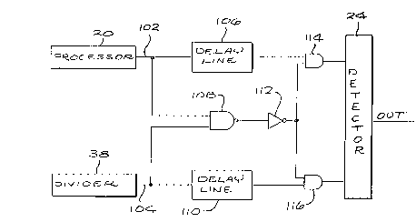
A system eliminates the adverse effects of serration
and equalization pulses (periodically generated during the
vertical sync interval) in regulating the frequency of
horizontal sync pulses. These sync pulses provide timing
information to regulate a video display. The system includes
circuitry for stripping and processing the horizontal and
vertical sync signals and the serration pulses from the video
signals. These pulses are introduced to a first AND gate and
through a first delay line to an input of a second AND gate.
Frequency divider output signals are introduced to the first
AND gate and to a third AND gate through a second delay line
having an equal delay with the first delay line. The output
from the first AND gate passes to second inputs of the second
and third AND gates. The second and third AND gates produce
signals which represent the time difference between the sync
and divider output signals and which have a maximum time
difference equal to the delays of the delay lines. In doing
so, the gates eliminate the effects of the serration and
equalization pulses. A phase comparator compares the times of
occurrence of the second and third AND gate signals and
introduces to a low pass filter the signals representing the
time difference. A voltage controlled oscillator produces a
signal having a frequency dependent upon the magnitude of the
output voltage from the filter. The frequency of the
oscillator signals is passed to a frequency divider. The
resultant divider signals are introduced to the first AND gate
and the second delay line.


Claims

Note: Claims are shown in the official language in which they were submitted.


THE EMBODIMENTS OF THE INVENTION IN WHICH AN EXCLUSIVE
PROPERTY OR PRIVILEGE IS CLAIMED ARE DEFINED AS FOLLOWS:
1. A system for regulating the frequency of an
oscillator to provide sync pulses for resolution of a video
image, comprising in combination:
first means for providing sync pulses controlling the
generation of horizontal and vertical retrace periods,
second means for providing comparison signals having a
time variable relative to the time of the sync pulses,
third means for providing a particular delay of the
sync pulses and of the comparison signals,
fourth means responsive to the sync pulses, the
comparison signals, the delayed sync pulses and the delayed
comparison signals for producing resultant pulses
representative, within particular limits dependent upon the
particular delay, of the difference in time between the sync
pulses and the comparison signals,
fifth means responsive to the resultant pulses for
producing an oscillatory signal having a frequency variable
in accordance with the occurrence of the resultant pulses,
and
sixth means for deriving the comparison signals in
accordance with the frequency of the oscillatory signal.
2. A system as set forth in claim 1, wherein the
fourth means produce the resultant pulses, within a time
period corresponding to the particular delay, after the
latter to occur of the sync and comparison pulses.
3. A system as set forth in claim 1 wherein the
fourth means increases the frequency of the oscillatory
signal when the sync pulses occur before the comparison
signals and the sixth means decreases the frequency of the
oscillatory signal when the comparison signals occur before
the sync pulses.


4. A system as set forth in claim 1, wherein the sync
pulses include serration pulses and wherein the fourth means
is operative to inhibit any effect of the serration pulses
in the production of the resultant pulses.
5. A system as set forth in claim 1, wherein the
fourth means are operative to inhibit any effect of noise
signals in the production of the resultant pulses.
6. A system for regulating the frequency of an
oscillator to provide sync pulses for resolution of a video
image, comprising in combination:
first means for providing sync pulses including
horizontal and vertical sync pulses and serration and
equalization pulses,
second means for providing comparison signals,
third means for delaying the sync pulses and the
comparison signals by a particular time interval,
fourth means responsive to the sync pulses, the
comparison signals, the delayed sync pulses and the delayed
comparison signals for producing control pulses having a
time interval dependent upon the relative times of
occurrence of the sync pulses and the comparison signals and
having a time interval dependent upon the particular time
interval,
fifth means responsive to the occurrence of the control
pulses for producing an oscillatory signal having a
frequency variable in accordance with such occurrence, and
sixth means responsive to the frequency of the
oscillatory signal for providing the comparison signals at
times dependent upon the frequency of the oscillatory
signal.


7. A system as set forth in claim 6, wherein the
fourth means include a first delay line for delaying the
sync pulses by the particular time interval and a second
delay line for delaying the comparison pulses by the
particular time interval and further include seventh means
responsive to the sync pulses, the comparison signals and
the delayed pulses from the first delay line to produce a
first output and further include eighth means responsive to
the sync pulses, the comparison signals and the delayed
signals from the second delay line to produce a second
output and where in the fifth means is responsive to the
outputs of the seventh and eighth means to produce the
oscillatory signal having the variable frequency.
8. A system as set forth in claim 7, wherein
the seventh means are operative only upon the simultaneous
occurrence of the sync pulses, the comparison signals and
the delayed sync pulses from the first delay line to produce
the first output and the eight means are operative only upon
the simultaneous occurrence of the sync pulses, the
comparison signals and the delayed comparison signals from
the second delay line to produce the second output.
9. A system for regulating the frequency of an
oscillator to provide sync pulses for resolution of a video
image, comprising in combination:
means for providing sync pulses from a video signal,
means for providing oscillatory signals having a
variable frequency,
means for providing a control signal having a duration
equal to the time between the sync pulses and the
oscillatory signals when this time duration is less than a
particular value and for providing a control signal having a
duration of the particular value when the time between the
sync pulses and the oscillatory signals is greater than the
particular value, and


means responsive to the control signal for adjusting
the frequency of the oscillatory signals in accordance
with the duration of the control signal.
10. In a system as set forth in claim 9, the control
signal means being operative to provide the control signal
with a polarity dependent upon whether the sync pulses occur
before or after the oscillatory signals, and
the adjusting means being operative to adjust the
frequency of the oscillatory signals upwardly or downwardly
in accordance with the polarity of the control signal.
11. In a system as set forth in claim 10,
the control signal means including means for providing
delays in the sync pulses and the oscillatory signals and
means for producing the control signal in accordance with
the relative times of occurrence of the sync pulses, the
oscillatory signals, the delayed sync pulses and the delayed
oscillatory signals.
12. A system as set forth in claim 11 wherein the
control means include a plurality of logical gates connected
in a particular logical relationship.
13. A system for regulating the frequency of an
oscillator to provide sync pulses for resolution of a video
image, comprising in combination:
means for providing sync pulses from a video signal,
means for providing oscillatory signals having a variable
frequency,
means responsive to the sync pulses and the
oscillatory signals for producing a control signal having a
polarity dependent upon the relative order in time of the
occurrence of the sync pulses and the oscillatory signals
and having a duration, limited to a particular maximum
value, dependent upon the relative times of occurrence of


the sync pulses and the oscillatory signals, and
means responsive to the control signals for varying the
frequency of the oscillatory signals in accordance with the
polarity and duration of the control signals.
14. In a system as set forth in claim 13, the control
signal means including means for providing a particular
delay to the sync pulses and to the oscillatory signals and
means for determining the time relationships between
particular pairs of the sync pulses, the oscillatory
signals, the delayed sync pulses and the delayed oscillatory
signals.
15. In a system as set forth in claim 13, the control
means including means for providing a particular delay to
the sync pulses and the oscillatory signals and means for
limiting the duration of the control signals to a time
corresponding to such particular delay.
16. A system as set forth in claims 14 or 15, wherein
the determining means include a NAND gate and AND gates
responsive to the sync pulses, the oscillatory signals, the
delayed sync pulses and the delayed oscillatory signals for
determining the polarity and duration of the control
signals.
17. A system for regulating the frequency of an
oscillator to provide sync pulses for resolution of a video
image, comprising in combination:
means for providing a video signal including
horizontal sync pulses and vertical sync pulses and
serration pulses,
means for providing an oscillatory signal having a
variable frequency,
means responsive to the sync pulses and the oscillatory
signals for producing, only upon the occurrence of the


horizontal sync pulses, control signals for a limited period
of time dependent upon the relative times of occurrence of
the horizontal sync pulses and the oscillatory signals, and
means responsive to the control signals for varying
the frequency of the oscillatory signals in accordance with
the characteristics of the control signals.
18. In a system as set forth in claim 17, the control
signal means including means for determining the polarity of
the control signals in accordance with the relative priority
of occurrence of the sync pulses and the oscillatory signals
and the frequency varying means including means for varying
the frequency of the oscillatory signals in accordance with
the polarity of the control signals.
19. In a system as set forth in claims 17 or 18, the
control means including means for providing aduration of the
control signals in accordance with the time difference
between the sync pulses and the oscillatory signals when
such time difference is less than the particular limit and
for providing a duration of the control signals at the
particular limit when such difference is at or greater than
the particular limit.
20. In a system as set forth in claims 17, 18 or 19,
means for delaying each of the sync pulses and the signals
by a time corresponding to the particular time limit and
means for combining individual pairs of the sync pulses, the
oscillatory signals, the delayed sync pulses and the delayed
oscillatory signals in a logical network relationship to
produce the control signals.

Description

Note: Descriptions are shown in the official language in which they were submitted.


20~~~~0
This invention relates to a system for generating
2 sync pulses in video signals representing video images. More
3 particularly, the invention relates to a system for
4 eliminating the effects of serration and equalization pulses
in generating sync pulses in video signals representing video
6 images.
7
8 Video images are generally represented by video
9 signals produced in a raster scan. In such a raster scan, a
horizontal sync pulse is produced at the beginning of the
11 video signals representing each horizontal line. A vertical
12 sync pulse is also produced at the end of the video signals
13 representing a complete image. When the vertical sync pulse
14 is produced, there is a relatively long blanking period during
which the beam producing the image is returned from the lower
lf> right corner of the screen to the upper left corner of the
L'7 screen so that a new raster scan can be initiated. During
lf3 this blanking period, serration and equalization pulses are
Zg produced periodically to define successive intervals in the
vertical blanking period.
21
22 One purpose of the sync pulse defining the beginning
23 of each horizontal line is to insure that the beginning of
24 each horizontal line occurs on a regulated basis such that the
beginning of the successive horizontal line will define a
26 straight vertical line. This assures that the image will be
27 displayed on the screen without any distortion. To accomplish
28 this, the rate of production of the horizontal sync pulses in
29 the video signal is regulated. However, the serration and
equalization pulses interfere with this regulation and
~'~l adversely affect the time for the production of the sync
;32 pulses. This prevents the image displayed on the video screen
1


2U7$'~40
1 from being as precise as might otherwise be desired. The
2 problems described in this paragraph have existed for a long
3 period of time without correction in spite of full knowledge
4 in the industry of the existence of this problem over such
period of time and consideration aver this period of time of
6 how to resolve the problem.
7
8 A system constituting one embodiment of this
9 invention eliminates the effects of serration and equalization
pulses (periodically generated during the vertical sync
11 interval) in generating output sync pulses to regulate the
12 timing of a video display. The system includes circuitry for
13 stripping and processing the horizontal and vertical sync
14 signals and the serration pulses from the video signals.
These pulses are introduced to an input of a first AND gate
7.G and through a first delay line to an input of a second AND
1'7 gate .
1B
19 Frequency divided oscillator signals are introduced
to the first AND gate and to an input of a second AND gate
21 through a second delay line providing a delay equal to that of
22 the first delay line. The output from the first AND gate
23 passes to second inputs of the second and third AND gates.
24 The second and third AND gates produce signals which represent
the time difference between the sync pulses and the divider
26 signals and which have a maximum time difference equal to the
27 delays of the delay lines. In doing so, the gates eliminate
28 the effects of the serration and equalization pulses.
29
A phase comparator compares the times of occurrence
31 of the second and third AND gate output signals and introduces
32 to a low pass filter the signals representing the results of
2

2~~~~~~
1 the comparison. A voltage controlled oscillator produces a
2 signal having a frequency dependent upon the magnitude of the
3 voltage from the filter. The oscillator signals are divided
4 by a frequency divider. The resultant signals constitute the
divider signals introduced to the first AND gate and to the
6 second AND gate through the first delay line and to the third
AND gate through the second delay line.
8
9 In the drawings:
11 Figure 1 is a circuit diagram, mostly in block form,
12 of a prior art sys'cem for generating sync pulses in a video
13 signal:
14 Figure 2 schematically shows timing diagrams
illustrating how the sync pulses are regulated by the system
lg of the prior art for regulating the time of occurrence between
.17 successive sync pulses;
18 Figure 3 illustrates how noise signals and serration
lg pulses adversely affect the time between the generation of
successive sync pulses by the system of the prior art;
21 Figure 4 is a circuit diagram (constituting one
22 embodiment of the invention) in block form for inclusion in
Z3 the system of Figure 1 to eliminate the adverse effects of the
24 noise signals and the serration and equalization pulses in
generating the successive sync pulses at the proper timing
26 intervals;
27 Figure 5 illustrates the generation of the
2g horizontal sync pulses and the vertical sync and serration and
2g equalization pulses in the stages prior to the circuitry shown
in Figure 4 and the generation of only the horizontal sync
31 pulses as a result of the operation of the circuitry shown in
32 Figure 4;
3

2~~$~40
Figure 6 schematically shows timing diagrams
2 illustrating the timing relationship of pulses produced at
3 strategic terminals in the circuitry shown in Figure 4 when
4 the pulses are produced within particular time limits
controlled by such circuitry;
6 Figure 7 schematically shows timing diagrams
7 illustrating the timing relationship of the pulses produced at
8 such strategic terminals when the pulses are produced outside
9 of such particular time limits;
Figure 8 shows timing diagrams illustrating how fast
11 the system of this invention responds to correct errors in the
12 timing of the horizontal sync pulses even during a vertical
13 retrace period when serration and equalization pulses are
14 produced.
16 A prior art circuit system is shown in Figure 1 and
17 generally illustrated at 10. The system 10 includes a
18 stripper 12 which receives a video signal on a line 14 and
lg strips the horizontal and vertical sync signals and the
serration and equalization pulses from the line. The
21 horizontal pulses are illustrated at 16 in Figure 3; the
22 vertical sync pulses are illustrated at 17 in Figure 3; and
23 the serration and equalization pulses are respectfully
24 illustrated at 18 and 19 in Figure 3. The horizontal sync
pulses 16 are produced at the beginning of each horizontal
26 line to provide a timing for the video signals in that line.
27 The vertical sync pulses 17 are produced at the end of the
28 scanning of the bottom horizontal line in a frame and until
29 the beam has been returned to the beginning of the scanning of
the top horizontal line. The serration pulses 18 are produced
31 during the vertical sync pulse 17 to provide a timing during
32 the vertical sync pulse. The equalization pulses 19 are
4

1 produced at the beginning and end of the vertical sync pulse.
2
3 The sync pulses from the stripper 12 are introduced
4 to a processor 20 which separates 'the horizontal and vertical
sync pulses and introduces these sync pulses to an input
6 terminal (A) of a phase detector 24 in a phase-locked loop
7 generally indicated at 26 in Figure 1 and shown in broken
8 lines in that Figure. The phase-locked loop 26 also includes
9 a low pass filter 28 shown within broken lines and
schematically illustrated by a resistor 30, a resistor 32 and
11 a capacitor 34 connected in series between the output of the
12 phase detector 24 and a reference potential such as ground.
13 The output voltage on the terminal common to the resistors 30
14 and 32 is introduced to a voltage controlled oscillator 36.
The output from the oscillator 36 in turn passes to a divider
7.6 38 which passes its output to another input (B) to the phase
L~Y detector 24.
1 f3
lg The phase detector 24 compares the phases of the
sync pulses from the processor 20 and a divided clock signal
21 from the divider 38. These signals are schematically
22 illustrated in Figure 2. For the case where the negative-
23 going edge of a sync pulse 40 from the processor 20 precedes
24 the negative-going edge of a signal 42 from the divider 38,
the phase detector 24 produces a positive signal 44. The
2g positive signal 44 is produced only during the period of time
27 between the negative edge of the pulse 40 and the negative
~g edge of the signal 42. The signal 44 may be considered as a
2g control or resultant signal.
31 The signal 44 is introduced to the filter 28 which
3N passes only the low frequency components in the signal. These
5

2~~~~~0
1 low frequency components cause the frequency of the signals
2 from the oscillator 36 to be increased. The oscillator 36
3 produces signals at a suitable frequency such as approximately
14.31818 megahertz. The frequency of this signal is divided
by a suitable divider such as 910 to produce signals at a
6 suitable frequency such as 15,750 kilohertz corresponding to
7 the frequency of the horizontal sync pulses 16. Since the
5 frequency of the oscillator signals introduced to the phase
9 detector 24 is increased, the phase difference between the
sync pulses from the processor 20 and the divider signals 44
11 is correspondingly reduced.
12
13 Figure 2 also illustrates the case where the
14 negative edge of the sync pulse 46 from the processor 20
follows the negative edge of the signal 48 from the divider
1.6 38. Under such circumstances, a voltage pulse 50 having a
1'l negative polarity is produced by the phase detector 24. This
1~ signal is produced only during the period between the negative
lg edge of the divider signal 48 and the sync pulse 46. This
2p signal is filtered by the filter 28 to produce the low
21 frequency components and these components are introduced to
22 the voltage controlled oscillator 36 to reduce the frequency
23 of the signals from the oscillator. After being divided in
24 frequency by the divider 38, these signals are introduced to
the phase detector 24 and the difference in time between the
26 sync pulses from the processor 20 and the frequency-divided
27 signals from the oscillator 36 is narrowed.
28
29 In this way, the frequency of the oscillator 36 is
regulated to provide the sync pulses at the desired rate for
31 providing a high resolution of the video image on a screen.
32 When the times of occurrence of the negative edges of the
6

~07~~40
1 pulses from the processor 20 and the frequency-divided signals
2 from the oscillator 36 are the same, no signal is introduced
3 to the oscillator so that the frequency of the signals from
4 the oscillator remains unchanged.
6 The problem with conventional sync circuits may be
7 readily seen from Figure 3. During the normal portion where a
8 video signal is being generated at the line 14, the sync
9 stripper 12 receives only the horizontal sync pulses 16 and
introduces these pulses to the processor 20. However, during
11 the vertical retrace interval, additional sync pulses pass
12 through the processor 12. These additional pulses are the
13 serration and equalization pulses respectively illustrated
14 schematically at 18 and 19 in Figure 3. These pulses occur at
times when no horizontal sync pulses 16 are being produced.
16
17 The pulses 18 cause the phase detector 24 to produce
18 positive pulses which increase the frequency of the oscillator
19 36. The phase detector 24 outputs a positive level until the
next horizontal sync pulse 16 is produced. The net effect of
21 the serration pulses 18 during the vertical retrace period is
22 to increase the frequency of the signals from the oscillator
23 36 even though no change in frequency is required. The start
24 of the first horizontal sync pulses in the next generation of
the video image on the video screen accordingly occurs at an
26 improper time. The equalization pulses 19 produce a similar
27 effect on the timing of the horizontal sync pulses 16.
~8
29 Figure 4 illustrates a circuit generally indicated
at 100 and constituting one embodiment of the invention. The
31 circuit 100 includes a line 102 for receiving sync pulses from
32 the processor 20 in Figure 1 and a line 104 for receiving
7

~~~$~40
1 frequency divided signals from the divider 38 in Figure 1.
2 The pulses on the line 102 pass to a delay line 106 providing
3 a suitable delay such as approximately four microseconds (4
4 sec.) and to an input terminal of an AND gate 108. The
signals on the line 104 pass to a delay line 110 also
6 providing a suitable delay such as approximately four
microseconds (4 sec.) and to a second input terminal of the
8 AND gate 108.
9
The output from the AND gate 108 passes to input
11 terminals of AND gates 114 and 116. A second input terminal
12 of the AND gate 114 receives signals from the delay line 106
13 and a second input terminal of the AND gate 116 receives
14 signals from the delay line 110. The output terminals of the
AND gates 114 and 116 are connected to the input terminals of
16 the phase detector 24 also shown in Figure 1.
17
18 Figure 5 shows horizontal sync pulses 120 in a first
row and the horizontal sync pulses and serration and
19
equalization pulses 122 in a second row. The pulses 120
effectively remain after the circuitry shown in Figure 4 has
21
operated to remove the serration and equalization pulses. The
22
operation of the circuitry shown in Figure 4 in removing the
23
serration pulses 122 (Figure 5) is illustrated by the examples
24
shown in Figures 6 and 7.
26
27 In the example shown in Figure 6, the sync pulses
130 from the processor 20 precede the divided oscillator
28
29 signals 132 from the divider 38 by a period of approximately
one (1) microsecond (l~sec.). This is indicated in Figure 6
31 by - 1. The sync pulses from the processor 20 are
32 indicated at A in Figure 6 to correspond to the input terminal
8


2~?8"~~0
1 A to the phase detector 24 in Figure 1. Similarly, the
2 signals from the divider 38 are indicated at B in Figure 6 to
3 correspond to the input terminal B to the phase detector 24 in
4 Figure 1. The delay lines 106 and 110 respectively delay the
signals 130 and 132 by four microseconds (4 sec.) as
6 indicated respectively at 134 and 136 in Figure 6. The AND
7 gate 108 in Figure 4 operates to pass a signal only when both
8 the sync pulses 130 and the divider signals 132 have reached a
9 positive level. Thus, the AND gate 108 operates to produce a
signal at the later of the times that a sync pulse 130 has
11 reached a positive level on the line 102 and a divider signal
12 132 has reached a positive level on the line 104.
13
14 The signal produced by the AND gate 108 is
introduced to the AND gate 114 as is the signal passing
16 through the delay line 106. The signal passing through the
17 AND gate 114 operates upon the phase detector 24 to obtain an
lg output from the phase detector. This output continues for a
lg maximum period of four microseconds (4 ~CSec.). Within this
period of four microseconds (4 ~tsec.), the delay line 110 will
21 introduce a signal to the AND gate 116. This signal passes
z2 through the AND gate 116 to the phase detector 24 to
23 inactivate the phase detector. The positive signal from the
24 phase detector 24 will have a width just equal to the time
difference between the A delayed output 134 and the B delayed
2g output 136. This positive signal causes the frequency of the
27 oscillatory signals from the oscillator 36 to increase,
2g thereby decreasing the period of time between the pulse on the
2g line 102 from the processor 20 and the signal on the line 104
from the divider 38.
'> 1
32
9


~o~~~~o
1 Figure 7 provides an example of the operation of the
2 circuitry of Figure 4 when the period between the pulse on the
3 line 102 and the divider signal on the line 104 exceeds four
4 microseconds (4 ,sec.), the period of the delay provided by
each of the delay lines 106 and 110. In the example shown in
6 Figure 7, the time between the pulse on the line 102 and the
7 signal on the line 104 is assumed to be five microseconds (5
8 sec.). This is illustrated by a pulse 160 on the line 102
9 and a signal 162 on the line 104 and is also indicated by -
5 between the rising edges of the pulses 160 and 162 in Figure
11 7. This causes the AND gate 108 in Figure 4 to provide an
12 output five microseconds (5 ~CSec.) after the signal is
13 provided on the line 102.
14
The output signal from the AND gate 108 in Figure 4
16 passes immediately through the AND gate 114 since the AND gate
:L7 has been previously prepared for activation by a signal from
lg the delay line 106. The output from the AND gate 114 is
lg illustrated at 164 in Figure 7. Four microseconds (4 sec.)
2p after the AND gate 114 starts to pass a signal, the delayed
21 signal on the line 104 passes through the AND gate 116. This
22 is indicated at 168 in Figure 7. This signal causes the phase
23 detector to be reset. Thus, the phase detector 24 output has
24 a positive level for a period of only four microseconds (4
~CSec.) even though the period of time between the pulse on the
26 line 102 and the signal on the line 104 exceeds four
27 microseconds (4 usec.). This is true whenever the signal on
28 one of the lines 102 and 104 precedes the signal on the other
29 line by a time period in excess of four microseconds (4~).
The circuitry shown in Figure 4 accordingly eliminates any
31 effect of serration pulses 18 or equalization pulses 119 in
32 the operation of the phase detector 24.


1 Figure 8 schematically illustrates the period of
2 time in which applicant's system responds to regulate the time
3 between the generation of successive sync pulses. In Figure
4 8, vertical retrace pulses are schematically illustrated at
200 and horizontal sync pulses are schematically illustrated
6 at 202. The output signals from the phase detector 24 are
7 schematically illustrated at 204. As will be seen, the
8 regulation in the operation of the phase detector 24 occurs in
9 only a few horizontal lines of the raster scan of a video
image.
11
12 The system described above has certain important
13 advantages. It regulates the frequency of the signal from the
14 voltage controlled oscillator 36 so that the horizontal sync
pulses occur at precisely controlled periods even during the
16 vertical retrace period and the time immediately after the
17 vertical retrace period. The system of this invention
la accomplishes this by eliminating any effects of serration and
lg equalization pulses on such regulation. The effects of
serration and equalization pulses on such regulation are
21 eliminated by producing control signals for regulating the
22 frequency of the signals from the voltage controlled
23 oscillator during the period between the sync pulses from the
24 processor 20 and the signals from the divider 30 when this
period is less than a particular value such as approximately
2g four microseconds (4 sec.). When the period of time between
27 the pulse on the line 102 and the signal from the divider 38
2g is greater than four microseconds (4 sec.), the activation of
29 the phase comparator 24 is limited to four microseconds (4
sec.).
31
32
11


1 Although this invention has been disclosed and
2 illustrated With reference to particular embodiments, the
3 principles involved are susceptible for use in numerous other
4 embodiments which will be apparent to persons skilled in the
art. The invention is, therefore, to be limited only as
6 indicated by the scope of the appended claims.
7
8
9
11
12
13
14
16
,r
is
19
21
22
23
24
2s
27
2a
29
31
32
12

Representative Drawing
A single figure which represents the drawing illustrating the invention.
Administrative Status

For a clearer understanding of the status of the application/patent presented on this page, the site Disclaimer , as well as the definitions for Patent , Administrative Status , Maintenance Fee  and Payment History  should be consulted.

Administrative Status

Title Date
Forecasted Issue Date 1999-12-14
(22) Filed 1992-09-21
(41) Open to Public Inspection 1993-03-27
Examination Requested 1997-01-22
(45) Issued 1999-12-14
Expired 2012-09-21

Abandonment History

There is no abandonment history.

Payment History

Fee Type Anniversary Year Due Date Amount Paid Paid Date
Application Fee $0.00 1992-09-21
Registration of a document - section 124 $0.00 1993-04-13
Maintenance Fee - Application - New Act 2 1994-09-21 $100.00 1994-09-20
Maintenance Fee - Application - New Act 3 1995-09-21 $100.00 1995-09-20
Maintenance Fee - Application - New Act 4 1996-09-23 $100.00 1996-09-18
Maintenance Fee - Application - New Act 5 1997-09-22 $150.00 1997-09-08
Maintenance Fee - Application - New Act 6 1998-09-21 $150.00 1998-09-02
Final Fee $300.00 1999-09-08
Maintenance Fee - Application - New Act 7 1999-09-21 $150.00 1999-09-21
Maintenance Fee - Patent - New Act 8 2000-09-21 $150.00 2000-09-05
Maintenance Fee - Patent - New Act 9 2001-09-21 $150.00 2001-08-31
Maintenance Fee - Patent - New Act 10 2002-09-23 $200.00 2002-09-03
Maintenance Fee - Patent - New Act 11 2003-09-22 $200.00 2003-09-03
Maintenance Fee - Patent - New Act 12 2004-09-21 $250.00 2004-09-01
Maintenance Fee - Patent - New Act 13 2005-09-21 $250.00 2005-09-01
Maintenance Fee - Patent - New Act 14 2006-09-21 $250.00 2006-08-30
Registration of a document - section 124 $100.00 2007-06-22
Maintenance Fee - Patent - New Act 15 2007-09-21 $450.00 2007-08-31
Maintenance Fee - Patent - New Act 16 2008-09-22 $450.00 2008-08-29
Maintenance Fee - Patent - New Act 17 2009-09-21 $450.00 2009-09-02
Maintenance Fee - Patent - New Act 18 2010-09-21 $450.00 2010-08-30
Maintenance Fee - Patent - New Act 19 2011-09-21 $450.00 2011-08-30
Owners on Record

Note: Records showing the ownership history in alphabetical order.

Current Owners on Record
BROOKTREE BROADBAND HOLDING, INC.
Past Owners on Record
BROOKTREE CORPORATION
COLLES, JOSEPH H.
Past Owners that do not appear in the "Owners on Record" listing will appear in other documentation within the application.
Documents

To view selected files, please enter reCAPTCHA code :


To view images, click a link in the Document Description column. To download the documents, select one or more checkboxes in the first column and then click the "Download Selected in PDF format (Zip Archive)" or the "Download Selected as Single PDF" button.

List of published and non-published patent-specific documents on the CPD .

If you have any difficulty accessing content, you can call the Client Service Centre at 1-866-997-1936 or send them an e-mail at CIPO Client Service Centre.


Document
Description 
Date
(yyyy-mm-dd) 
Number of pages   Size of Image (KB) 
Cover Page 1994-02-26 1 13
Claims 1999-05-18 6 251
Drawings 1999-05-18 3 51
Cover Page 1999-12-07 1 47
Abstract 1994-02-26 1 43
Claims 1994-02-26 7 229
Drawings 1994-02-26 3 47
Description 1994-02-26 12 465
Representative Drawing 1998-10-26 1 3
Representative Drawing 1999-12-07 1 6
Assignment 2008-02-26 6 163
Correspondence 1999-09-08 1 28
Assignment 2007-06-22 5 144
Prosecution Correspondence 1993-02-26 2 55
Prosecution Correspondence 1997-01-22 1 27
Prosecution Correspondence 1998-10-02 2 65
Examiner Requisition 1998-06-02 1 39
Fees 1996-09-18 1 42
Fees 1995-09-20 1 81
Fees 1994-09-20 1 57