Note: Descriptions are shown in the official language in which they were submitted.
2079129
This invention relates to a power amplifying
circuit, such as a final stage amplifier of a radio
transmitter, for amplifying an input signal having an
electric power in response to an amplification control signal
to produce an output signal having an amplified electric
power.
The power amplifying circuit is particularly useful
in a base station of a mobile radio communication network.
In the mobile radio communication network, a mobile
station usually moves in a service area of the base station.
A distance between the base station and the mobile station is
therefore variable. If the base station transmits a radio
signal produced by a usual power amplifying circuit to have
a fixed or predetermined electric power, the mobile station
receives the radio signal with a variable electric power
depending on the distance.
In the manner which will later be described in more
detail, a conventional power amplifying circuit amplifies the
input signal having the electric power in response to an
amplification control signal to produce an output signal
having an amplified electric power. The control signal
controls the amplified electric power so as to keep an
electric power of the received radio signal fixed. The
conventional power amplifying circuit is defective in that it
is impossible to produce the output signal having a desired
waveform in a wide range.
*
.~
207~1~9
It is therefore an object of the present invention
to provide a power amplifying circuit capable of producing an
output signal having a desired waveform in a wide range.
Other objects of this invention will become clear
as the description proceeds.
On describing the gist of this invention, it is
possible to understand that a power amplifying circuit is for
amplifying an input signal having an input electric power in
response to an amplification control signal to produce an
output signal having an amplified electric power and includes
(a) a power amplifier for amplifying the input electric power
into the amplified electric power, (b) a detector connected
to the power amplifier for detecting the amplified electric
power to produce a detection signal, (c) power control signal
generating means for generating a power control signal based
on the amplification control signal, (d) a comparator
connected to the detector and the power control signal
generating means for comparing the detection signal and the
power control signal to produce an error signal, and (e) a
driver connected to the comparator and the power amplifier
for driving the power amplifier based on the error signal.
According to this invention, the above-understood
power amplifying circuit comprises a reference signal
generator for generating a reference signal with a
predetermined waveform, and a multiplier connected to the
power control signal generating means, the reference signal
2079129
generator, and the comparator for multiplying the power
control signal and the reference signal and for producing a
level control signal as the power control signal.
Embodiments of the invention will now be described
by way of example, with reference to the accompanying
drawings, in which:
Figure 1 is a block diagram of a conventional power
amplifying circuit;
Figure 2 is a block diagram of a power control
signal generator for use in the power amplifying circuit
illustrated in Figure 1;
Figure 3 is a block diagram of another power control
signal generator for use in the power amplifying circuit
illustrated in Figure 1;
Figure 4 shows an expected waveform of an output
signal of a power amplifying circuit in general;
Figure 5 shows a waveform of an output signal of the
radio receiver illustrated in Figure 1;
Figure 6 is a block diagram of a power amplifying
circuit according to an embodiment of this invention;
Figure 7 is a block diagram of a power control
signal generator for use in the power amplifying circuit
illustrated in Figure 6; and
Figure 8 shows a waveform of an output signal of the
power amplifying circuit illustrated in Figure 6.
2079129
Referring to Figure 1, a conventional power
amplifying circuit will first be described in order to
facilitate an understanding of the present invention. The
power amplifying circuit is for amplifying an input signal
having an electric power in response to an amplification
control signal to produce an output signal having an
amplified electric power.
In Figure 1, the power amplifying circuit comprises
a power amplifier 11 having an input terminal 12 and an
output terminal 13. The power amplifier 11 is for amplifying
the input electric power into the amplified electric power.
A detector 14 is connected to the output terminal 13 of the
power amplifier 11 for detecting the amplified electric power
to produce a detection signal. A power control signal
generator 15 has an amplification control signal input
terminal 16 and is for generating a power control signal
based on the amplification control signal. A comparator 17
is connected to the detector 14 and the power control signal
generator 15 for comparing the detection signal and the power
control signal to produce an error signal. A driver 18 is
connected to the comparator 17 and the power amplifier 11 for
driving the power amplifier 11 based on the error signal.
The input signal is supplied to the input terminal
12. The power amplifier 11 amplifies the input electric
power into the amplified electric power. The power amplifier
11 supplies the output signal to the output terminal 13. The
,.:' `''
2079129
power amplifier 11 has a gain controlled by a driving signal
supplied from the driver 18.
The detector 14 detects the amplified electric power
to produce the detection signal. The detector 14 supplies
the detection signal to the comparator 17.
The amplification control signal input terminal 16
is connected to a power controller (not shown). The power
controller supplies the amplification control signal to the
amplification control signal input terminal 16. The power
control signal generator 15 produces the power control signal
in response to the amplification control signal for supply to
the comparator 17.
The comparator 17 compares the detection signal and
the power control signal to produce the error signal. The
comparator 17 supplies the error signal to the driver 18.
The driver 18 drives the power amplifier 11 based
on the error signal. A gain of the power amplifier 11
depends on the error signal.
Referring to Figure 2, the power control signal
generator 15 will be described more in detail. In Figure 2,
the power control signal generator 15 comprises a shift
register 15A for converting a serial N-bit data into a
parallel N-bit data. The parallel N-bit data are supplied to
first through N-th switches 15Bl, 15B2, ..., and 15BN, where
N represents a predetermined positive integer. An n-th
switch 15Bn is supplied with one bit of the parallel N-bit
2079129
data at a time, where n is variable between 1 and N, both
inclusive. The switches 15 (suffix omitted) are supplied in
common with electric power through a power supplying resistor
15C from a power source indicated by a horizontal short line
and individually grounded by grounding resistors 15Dl, 15D2,
..., and 15DN, respectively.
The amplification control signal is the serial N-bit
data. Each bit of the N-bit data has a low or a high level.
The n-th switch 15Bn is turned on to an on state, if the bit
is supplied thereto with the high level. The n-th switch
15Bn is turned off to an off state, if the bit is supplied
with the low level. The power control signal generator 15
produces the power control signal which is decided by a
resistance of the power supplying resistor 15C, resistance of
the grounding resistors 15Dl, 15D2, ..... , and 15DN, and the on
and the off states of the switches 15.
Referring to Figure 3, another power control signal
generator 15 comprises a shift register 15J for converting a
serial N-bit data into a parallel N-bit data for use as an
address data. A read-only memory 15K is connected to the
shift register 15J and memorizes digital power control
signals for producing one of the digital power control
signals in response to the address data. A digital/analog
converter 15L is connected to the read- only memory 15K for
converting the digital power control signal into an analog
power control signal. A low pass filter 15M is connected to
2079129
the digital/analog converter 15L for filtering the analog
power control signal.
When used in a time division multiple access
transmitter, the power amplifying circuit must produce the
power control signal which has in general a waveform having
smooth rise and fall exemplified in Figure 4. This is in
order to suppress a broadening of a spectrum of an output
signal of the power amplifying circuit when the switches 15
are put into the on and off states. In Pan-European mobile
telephone system (GSM), the power amplifying circuit must
control electric power of the output signal in a range
between 30 dB and 42 dB.
The conventional power amplifying circuit with the
power control signal generator 15 shown in Figure 2 is
difficult to exactly control the electric power in a wide
range of 30 dB to 42 dB. The conventional power amplifying
circuit with the power control signal generator 15 shown in
Figure 3 does not produce an output signal having an expected
waveform when the electric power is 40 dB. This is because
the read-only memory 15K has a narrow dynamic range. In this
case, the waveform of the output signal is depicted in Figure
5.
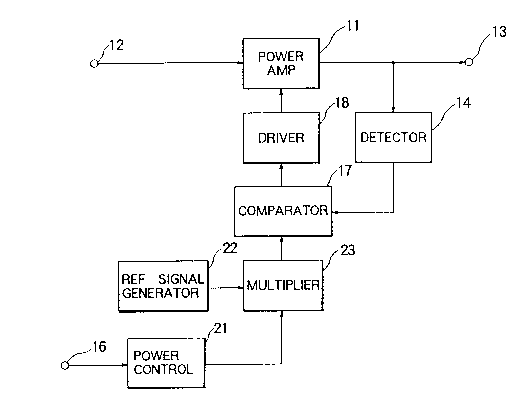
Referring to Figure 6, the description will proceed
to a power amplifying circuit according to a preferred
embodiment of this invention. Similar parts are designated
by like reference numerals.
~'
207gl29
The power amplifying circuit is for amplifying an
input signal having an input electric power in response to an
amplification control signal to produce an output signal
having an amplified electric power. The power amplifying
circuit includes a power amplifier 11 for amplifying the
input electric power into the amplified electric power. A
detector 14 is connected to the power amplifier 11 for
detecting the amplified electric power to produce a detection
signal. A power control signal generator 21 is for
generating a power control signal based on the amplification
control signal. A comparator 17 is connected to the detector
14 and the power control signal generator 21 for comparing
the detection signal and the power control signal to produce
an error signal. A driver 18 is connected to the comparator
17 and the power amplifier 11 for driving the power amplifier
11 based on the error signal.
The power amplifying circuit comprises a reference
signal generator 22 for generating a reference signal with a
predetermined waveform. A reference signal generator 22 is
described as an envelope generator in United States Patent
No. 4,706,262. A multiplier 23 is connected to the power
control signal generator 21, the reference signal generator
22, and the comparator 17 for multiplying the power control
signal of the power control signal generator 21 and the
reference signal supplied from the reference signal generator
to supply a level control signal as the power control signal
2079129
to the comparator 17. For example, the multiplier 23 is an
analog multiplier NJM4200 which is made by New Japan Radio
Corporation.
Turning temporarily to Figure 7, the power control
signal generator 21 comprises a shift register 21A for
converting a serial N-bit data into a parallel N-bit data for
use as an address data. A read-only memory 21B is connected
to the shift register 21A and memorizes digital power control
signals for producing one of the digital power control
signals in response to the address data. A digital/analog
converter 21C is connected to the read-only memory 21B for
converting the digital power control signal into an analog
power control signal for use as a direct voltage signal.
Turning back to Figure 6, the reference signal
generator 22 produce the reference signal which has a
waveform as depicted in Figure 4. The waveform is always
kept at a fixed form.
The multiplier 23 receives the analog power control
signal and the reference signal and produce the level control
signal. The level control signal has a waveform which is
similar to the waveform of the reference signal. The level
control signal has an amplitude which corresponds to a
voltage of the analog power control signal.
Turning to Figure 8(a), it will be assumed that the
analog power control signal has a voltage Vl. In this event,
the level control signal has an amplitude Vl and has a
2079129
waveform which is similar to the waveform of the reference
signal. In Figure 8(b), it will be assumed that the analog
power control signal has a voltage V2. In this event, the
level control signal has an amplitude V2 and has a waveform
which is similar to the waveform of the reference signal.
Turning back again to Figure 6, the detector 14
detects the amplified electric power to produce the detection
signal. The comparator 17 receives the detection signal and
the power control signal and produces the error signal. The
comparator 17 supplies the error signal to the driver 18.
The driver 18 drives the power amplifier 11 based on the
error signal. The power amplifier produces the output signal
having the amplified electric power. The power amplifier 11
has a gain depending on the error signal. The power
amplifying circuit can produce the output signal having an
expected waveform at a wide range of the gain.