Note: Descriptions are shown in the official language in which they were submitted.
2079554
HIGH POWER FACTOR AC/DC CO~V~Kl~K
BACKGROUND OF THE INVENTION:
Field of The Invention
The present invention relates generally to a
circuit of AC/DC converter which converts a commercially
available alternating current power supply voltage into a
stable DC output voltage, particularly, relates to the
AC/DC converter having a high power factor.
Description of The Background Art
Fig. l shows a conventional AC/DC converter
which converts the received commercially available
alternating current (AC) power supply into a direct
current (DC) voltage.
In Fig. l, the AC/DC converter includes an
input rectifying circuit RCl which carries out a full
rectification of an input alternating current voltage Ei,
a smoothing capacitor Cl, a field effect transistor Ql
which serves as a switching device, a transformer Trl,
transformer magnetically resetting diode D4, an output
rectifying diode D2, a flywheel diode D3, an output
smoothing choke coil L2, and an output smoothing
capacitor C2. Thus, the AC/DC converter serves to
convert the alternating input voltage Ei into a stable DC
output voltage Eo.
Although, in such an AC/DC converter as
described above, a desired characteristic is exhibited
for the output DC voltage, the input current thereof Ii
flows only at a time at which a peak of the instantaneous
input alternating current voltage Ei approximately
appears as appreciated from Fig. 2.
Therefore, a power factor of the AC/DC
converter shown in Fig. l is as low as about 0. 5 through
0. 7.
To improve the power factor, a method of
2079554
inserting a large sized choke coil into the rectifying
circuit has been proposed. However, the size and weight
of the AC/DC converter are too large and heavy.
Another method for improving the power factor
is to install a pre-converter to electronically improve
the power factor has been proposed. However, the other
method introduces the increased number of parts and
components, large-sized and expensive AC/DC converter,
and interferences between the switching devices in the
10 AC/DC converters.
SUMMARY OF THE INVENTION:
It is, therefore, a principal object of the
present invention to provide a structure of AC/DC
converter which is simple in circuit structure, small in
size, light in weight, and sufficiently economical.
The above-described object can be achieved by
providing an AC/DC converter, comprising; a) a pair of
input terminals to be connected across a commercially
available AC power supply; b) a full wave rectifying
circuit having a pair of input.terminals connected across
the pair of input terminals of the AC power supply and
having a pair of rectified output terminals; c) a first
choke coil having one terminal connected to one of the
pair of the rectified output terminal of the full wave
rectifying circuit; d) a first capacitor one end
connected to the other terminal of the first choke coil;
e) a first diode whose anode terminal is connected to
the other end of the first choke coil; f) a control
circuit for generating an on and off drive signal having
a relatively high frequency as compared with a frequency
of the AC power supply; g) a second capacitor one end
thereof connected to its cathode terminal of the first
diode and the other end connected to the other of the
pair of the rectified output terminal; h) switching
means having a pair of main electrodes and drive
~ 2079~54
electrode terminals, its drive electrode terminal being
driven in response to the on and off drive signal by
means of the control circuit so that said switching means
is turned on and off, one of the main electrodes being
connected to the other end of the first capacitor, and
the other main electrode being connected to the other end
of the second capacitor;i) a transformer having at least
primary winding and secondary winding, one end of its
primary winding connected to the cathode of the first
0 diode and the other end of the primary winding being
connected to the other end of the first capacitor; and j)
rectifying means connected across the secondary winding
of the transformer, the rectifying means having a pair
of output terminals of the AC/DC converter.
The above-described object can also be achieved
by providing an AC/DC converter, comprising: a) a pair of
input terminals to be connected to a commercially
available single phase AC power supply; b) a full wave
rectifying circuit having a pair of input terminals
connected across said pair ~f input terminals to be
connected to the commercially available AC power supply
and having a pair of plus and minus rectified output
terminals; c) a smoothing capacitor having a plus end
connected to the plus rectified output terminal of the
full wave rectifying circuit and a minus end connected to
the minus rectified output terminal thereof; d) a
transformer having at least one primary winding and
secondary winding; e) switching means having a pair of
main electrodes and a drive electrode, both main
electrodes being connected between said primary winding
and the minus rectified output terminal of said full wave
rectifying circuit, being turned on when the drive
electrode receives an on drive signal, and being turned
off when the drive electrode receives an off drive signal
and a frequency of said on and off drive signals being
2079~51
.
-- 4 --
higher than the frequency of said commercially available
AC power supply; f) an inductor providing a constant
current supply connected between the plus rectified
output terminal of said full wave rectifying circuit and
a positive end of said primary winding ; g) a diode
interposed between the first inductor and the positive
end of said primary winding for blocking a current flow
from said primary winding into said inductor; h) a
capacitor interposed between a junction between said
~o first inductor and a negative end of said primary
winding, said eapacitor being charged according to a
current flow from said inductor until its terminal
voltage is equal to a terminal voltage across the
smoothing capacitor when said main electrodes of said
switching means are turned on so that the current energy
is stored therein and a stored charge in said smoothing
capacitor is supplied to said primary winding and its
terminal voltage across said capacitor being reversed and
said transformer being reset when a current route is
formed in a loop in which the current energy is caused to
flow from said primary winding, capacitor, and diode
while said smoothing capacitor is charged via said diode
when said main electrodes of said switching means are
turned off; and i) another rectifying circuit connected
across the secondary winding of said transformer for
providing a DC output voltage across a pair of output
terminals of the AC/DC converter.
The above-described ob~ect can also be achieved
by providing an AC/DC converter, comprising; a) an AC
power supply; b) a full wave rectifying circuit having a
pair of input terminals connected across the AC power
supply and having a pair of rectified output terminals;
c) a first choke coil having one terminal connected to
one of the pair of the rectified output terminal of the
full wave rectifying circuit; d) a first capacitor one
2079554
end connected to the other terminal of the first choke
coil; e) a first diode whose anode terminal is connected
to the other end of the first choke coil; f) a control
circuit for generating an on and off drive signal having
a relatively high frequency as compared with a frequency
of the AC power supply; g) a second capacitor one end
thereof connected to its cathode terminal of the first
diode and the other end connected to the other of the
pair of the rectified output terminal; h) switching
0 means having a pair of main electrodes and drive
electrode terminals, its drive electrode terminal being
driven in response to the on and off drive signal by
means of the control circuit so that said switching means
is turned on and off, one of the main electrodes being
connected to the other end of the first capacitor, and
the other main electrode being connected to the other end
of the second capacitor; i)-a transformer having at least
primary winding and secondary winding, one end of its
primary winding connected to the cathode of the first
diode and the other end of the primary winding being
connected to the other end of the first capacitor; and j)
rectifying means connected across the secondary winding
of the transformer, the rectifying means having a pair
of output terminals of the AC/DC converter.
BRIEF DESCRIPTION OF THE DRAWINGS:
Fig. l is a conventional AC/DC converter
described in the BACKGROUND OF THE INVENTION.
Fig. 2 is a waveform chart of the input AC
current (Ii) and AC voltage (Ei) of the AC/DC converter
shown in Fig. l.
Fig. 3 is a circuit diagram of an AC/DC
converter in a first embodiment according to the present
invention.
Figs. 4 (A) through 4 (G) are waveform charts
for explaining an operation of the first embodiment shown
207955~
\
- 6 -
in Fig. 3.
Fig. 5 is a waveform chart of the input AC
voltage and AC current to the AC/DC converter shown in
Fig. 3.
5Fig. 6 is a circuit diagram of an AC/DC
converter in a second embodiment according to the present
invention.
Figs. 7 (A) through 7 (G) are waveform charts
for explaining an operation of the AC/DC converter in the
10 second embodiment shown in Fig. 6.
Fig. 8 is a circuit diagram of the AC/ DC
converter in a third embodiment according to the present
invention.
Figs. 9 (A) through 9 (C) are waveform charts
for explaining an operation of the third embodiment shown
in Fig. 8.
Figs. 9 (D) through 9 (F) are waveform charts
of the input AC currents in the case of the third
embodiment shown in Fig. 8.
20Fig. lO is a circuit wiring diagram of the
AC/DC converter in a fourth embodiment according to the
present invention.
Fig. ll is a circuit wiring diagram of the
AC/DC converter in a fifth embodiment according to the
present invention.
Fig. 12 is a waveform chart for explaining an
operation of the AC/DC converter shown in Fig. ll.
Fig. 13 is a characteristic graph representing
a relationship between the operating frequency of the
AC/DC converter shown in Fig. ll and transfer energy
thereof.
Fig. 14 is a circuit diagram of the AC/DC
converter in a sixth embodiment according to the present
invention.
DESCRIPTION OF THE PREFERRED EMBODIMENTS:
2079554
Reference will hereinafter be made to the
drawings in order to facilitate a better understanding of
the present invention.
It is noted that Figs. l and 2 have already
been explained in the BACKGROUND OF THE INVENTION.
(First Embodiment)
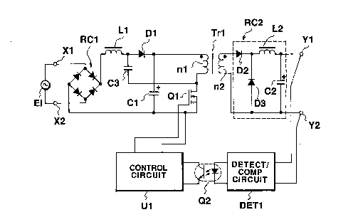
Fig. 3 shows a first embodiment of an AC/DC
converter according to the present invention.
In Fig. 3, a commercially available AC power
10 supply Ei is connected across a bridge type (full wave)
rectifier RCl via input terminals Xl and X2.
A positive DC output terminal of the rectifier
RCl is connected to a plus end of a capacitor Cl via a
choke coil (having a core) Ll and diode Dl and a
negative DC output terminal of the rectifier RCl is
connected to a minus end of the capacitor Cl. A junction
between the choke coil Ll and diode Dl is connected to a
drain electrode of a field effect transistor Ql via a
capacitor C3. Its source electrode of the transistor Ql
is connected to the minus end o,f the capacitor Cl. A gate
electrode of the transistor Ql is connected to a control
circuit Ul which serves as a switching regulator so that
the transistor Ql is driven to turn ON and OFF in
response to a drive signal derived from the control
circuit Ul at a high frequency of about lOO KHz.
The above-described portion of the circuitry
serve as a rectifying chopper circuit.
In details, while the input AC voltage Ei
(generally, in Japan, lOO V effective value and 50 Hz
East half of Japan) is rectified by means of the
rectifier RCl and rectified voltage is supplied across
the transistor Ql via the choke coil Ll and capacitor C3.
The transistor Ql repeats the ON and OFF operations at
the frequency of about lOO KHz. For exmple, in the first
embodiment, the choke coil Ll has an inductance of about
2079554
500 ~H (micro Henry) and the capacitor C3 has a
capacitance of 0. 02 ~F (micro Farad), and the capacitor
Cl has the capacitance of 200 ~F.
When the transistor Ql is turned on, the input
AC rectified current flows from the choke coil Ll to
charge the capacitor C3. This current flows during an
interval of time until a voltage across the capacitor C3
reaches a voltage across the capacitor Cl so that an
energy (power) is stored in the choke coil Ll and
0 capacitor C3. When the field effect transistor Ql is, in
turn, turned off, the current energy stored in the choke
coil Ll charges the capacitor Cl via the diode Dl.
Since an electrostatic capacitance of the
capacitor Cl has a sufficiently large value, the
substantially constant voltage Eb is maintained across
the capacitor Cl in a steady state. In addition, since
the input AC current always passes through the choke
coil Ll, the current is continued.
Next, the plus input end of the capacitor Cl is
connected to the drain electrode of the transistor Ql via
a primary winding nl of the transformer Trl.
A secondary winding n2 of the transformer Trl
is connected to a smoothing capacitor C2 via a smoothing
choke coil L2 and a diode D2 and connected across output
DC terminals Yl and Y2.
A detection/comparison circuit DETl is
connected across the DC output terminals Yl and Y2.
It is also noted that output terminals of the
detection/comparison circuit DETl are coupled with a
photo coupler Q2 which is optically connected to
detection input ends of the control circuit Ul.
The detectionicomparison circuit DETl is
generally constituted by a switching regulator IC, e.g.,
TL494 of Texas Instrument, Inc. available on the market
or an equivalent IC to which an output current amplifier
" "`` 2079554
and some auxiliary parts are added.
In addition, the detection/comparison circuit
DETl is constituted by a resistance divider and constant
voltage (zener) diode. Then, the photo-coupler Q2 has a
sufficient withstanding voltage to isolate the
commercially available AC current power supply Ei.
A flywheel diode D3 is connected across a
junction between the diode D2 and the smoothing choke
coil L2 and the other end of the secondary winding n2 of
0 the transformer Trl. This portion serves as a forward
type converter and is used to reset the transformer Trl
through an inherent vibration (resonance vibration)
between the primary winding nl of the transformer Trl and
capacitor C3.
While the transistor Ql is turned on, the
stored charge across the capacitor Cl serves to supply
the power to the output terminals Yl and Y2 via the
primary winding nl of the transformer Trl and successive
circuit stage. While the transistor Ql is turned off,
the current energy flowing thrQugh the primary winding nl
of the transformer Trl flows via a route of capacitor C3
and diode Dl to reset the transformer Trl and to reverse
the voltage across the capacitor C3.
Next, an operation of the first embodiment
z5 shown in Fig. 3 will be described below with reference to
Figs. 4 (A) through Fig. 5.
Suppose that a switching frequency of the
transistor Ql is sufficiently higher than the frequency
of the input AC voltage power supply. Hence, the input
AC voltage during one cycle of the switching operation of
the transistor Ql is deemed to be constant. In addition,
since the choke coil Ll has a large inductance with
respect to the switching frequency of the transistor Ql,
the choke coil Ll provides a constant current supply.
Furthermore, a self inductance of the transformer Trl is
2079554
- 10 -
considerably small as compared with that of the choke
coil L1 and winding ratio thereof is 1 : 1. The
inductance of the choke coil L2 is sufficiently large and
the output filtering choke coil L2 provides a current
5 SUpp ly .
The operation of the first embodiment shown in
Fig. 3 will be described in details below with time
intervals divided into TO, T1, , T7 shown in Figs. 4
(A) through 4 (G).
0 [Time interval from TO to T1]
When the field effect transistor Q1 is turned
on at a time of TO, the current flowing in a closed loop
of Ei ~ L1 ~ C3 ~ nl ~ C1 ~ Ei is, in turn, caused
to flow into the transistor Q1 via the capacitor C3. At
15 the same time, the voltage Eb across the capacitor C1 is
applied across the primary winding nl of the transformer
Trl and the same voltage is generated across the
secondary winding n2 so that the current which has flown
into the choke coil L2 is wholly commutated into the
20 secondary winding n2. Hence, the current of the primary
winding nl of the transformer Trl exhibits a stepwise
change of the current which has flown into the diode D3,
as shown in Eig. 4 (A), at the time of TO and,
thereafter, the current of the primary winding nl is
25 raised at a gradient of Eb/LO (LO denotes the self
inductance of the transformer Trl). Then, the current il
flowing through the choke coil L1 is expressed as
follows:
il = J sin (~ 1t + a) ~ (1), wherein
~ J 10 + ~12C32(Ei + VCo)2
a = tan~1 J1o/ ~1C3(Ei + VCO)
~1 = 1 / L1 C 3
2079554
- 11 -
J1o denotes an initial current flowing through
the choke coil L1,
VcO denotes an initial voltage across the
capacitor C3, and
5C3 denotes a capacitance across the capacitor
C3.
In the equation (1), the initial value of i1 is
different depending on a phase of the input AC voltage
Ei. J1o becomes larger as the input voltage Ei becomes
0 higher. Conversely, as the input voltage Ei becomes
higher, the value of VcO becomes smaller.
Hence, a provides a larger value as the phase
of the input voltage Ei provides a higher value from zero
to peak (90 degrees). That is to say, a provides
generally 50 degrees to 80 degrees when the level of the
alternating input voltage changes from zero to peak. In
addition, the interval time of T1 ~ T 2 is an interval of
time within which the capacitor C3 is charged until its
voltage reaches the voltage Eb. The completion of
charging becomes earlier, at the phase of the
instantaneous alternating voltage which provides a higher
value. Therefore, at the time of the present phase at
which the input instantaneous alternating voltage gives a
lower value, the time interval of t1 to t2 becomes as
long as approximately 1.5 ~ 5 ~S.
The waveform of input current Ic3 is shown in
Fig. 4 (B). Then, the voltage Vc3 across the capacitor C3
is raised substantially linearly as shown in Fig. 4 (D).
The current IQ flowing into the field effect transistor
Q1 is a sum of the current In1 flowing into the winding
nl and that Ic3 flowing through the capacitor C3 (refer
to Fig. 4 (C)). The current In2, flowing through the
secondary winding of the transformer Trl, is partially
derived from the current which has flown into the diode
D3 so as to make equal to the output current I0 as shown
` 2079S~l
. ,
in Fig. 4 (E).
[Time Interval of Tl - T2]
At the time of Tl at which the voltage across
the capacitor C3 becomes equal to the voltage Eb of the
capacitor Cl, the voltage thereacross is clamped to Eb so
that the current in the choke coil Ll flows into the
capacitor Cl via the diode Dl. Hence, the current IQ
flowing through the field effect transistor Ql continues
to rise at the gradient of Eb/L0 although the current
flowing through the capacitor C3 becomes null.
In addition, the output current Io is supplied
via the transformer Trl from the capacitor Cl of the
AC/DC converter shown in Fig. 3.
The current il flowing through the choke coil
Ll is expressed in the following equation (2) provided
that the voltage across the capacitor C3 is constant.
il = (Ei - Eb)t/Ll + J20 ---~ (2)
, wherein J20 denotes an initial current of the
choke coil Ll at the time of T,l.
The current il is reduced according to the
equation (2) since the value of Eb is always higher than
that of Ei. As the instantaneous input voltage Ei gives
higher value at the present phase, the reduction gradient
is moderate.
This operation mode is continued until T3 at
the time of which the field effect transistor Ql is
turned off. A conduction interval of the transistor Ql
is generally constant if a load and effective value of
the input voltage remain unchanged. This interval of time
becomes longer as the instantaneous input voltage has a
higher value at the present phase, i.e., approximately 0
through 3. 5 ~S.
[Time Interval of T2- T3]
When the field effect transistor Ql is turned
2079~54
- 13 -
off at the time of T2, the energizing current which has
flown in the primary winding nl is, in turn, caused to
flow in a closed loop of nl ~ C3 ~ D1 ~ nl.
The voltage across the transistor Q1 is
increased from zero in accordance with the voltage across
the capacitor C3 (refer to Fig. 4 (F)). The current
flowing in the secondary winding n2 of the transformer
Trl is continued to flow since the voltage across the
capacitor C3 is applied to the primary winding nl of the
10 transformer Trl even after the transitor Q1 is turned
off. Then, the current of the choke coil L1 is continued
to be decreased and to flow through the capacitor C1 as
expressed in the equation (2). At this time, the current
i3 flowing into the capacitor C3 is given by:.
i3 = -~ (~ 3C3Eb)2 + K302sin(~ 3t + r) - Io
--- (3), wherein
~ 32 = l/Lo C3
r = tan~1(k30/~2C3Eb)
K30 denotes the initial current of L0 (a value
20 Of subtraction of the output current from the primary
winding current at the time of T2) and,
lo denotes the output current of the AC/DC
converter.
In the equation (3), since K30 indicates a
large value, the value of r gives approximately 70
degrees and the change in the current i3 becomes minor
and is deemed to substantially be constant. This
operation mode is continued until the voltage across the
capacitor C3 becomes zero. The time interval of T2 ~
T3 indicates 1 ~S or less.
[Time interval T3 - T5]
When the voltage across the capacitor C3
indicates zero at the time of T3 as shown in Fig. 4 (D),
the voltage across the primary winding nl of the
transformer Trl also indicates zero so that the current
2079~
of the secondary winding n2 is interrupted and the
current of the choke coil L2 is continued to flow via the
flywheel diode D3.
Hence, the current through the primary winding
Inl of the transformer Trl is decreased by the output
current Io at the time of T3 as shown in Fig. 4 (A) and,
thereafter, a free vibration between the energization
inductance Lo and capacitance C3 is continued so that the
voltage across the capacitor C3 is reversed and becomes
0 negatively larger. Then, the voltage across the field
effect transistor Ql is continued to rise in accordance
with the voltage across the capacitor C3.
At the time of T4, the direction of the
current Inl flowing into the primary winding nl is
reversed and the voltage Vc3 across the capacitor C3
reaches a negative peak value (refer to Fig. 4 (D)) so
that the voltage Vc3 thereacross continues the vibration
until the time reaches T4 at which the current Inl of
the primary winding nl equals to that of the choke coil
Ll. Hence, the current Ic3 fl~wing into the capacitor C3
indicates the current i3 of the equation (3) to which Io
is added. A time duration between the time T3 and T4
indicates approximately 2 ~S or longer without influence
of the input voltage phase. The time duration between T4
and T5 becomes longer as the input current becomes
larger. Therefore, the time duration between T4 and T5
becomes longer when the present phase is such that the
instantaneous input voltage becomes higher. The
difference between the time durations described above
indicates about l ~S.
[Time interval of T5 - T6]
When the current in the choke coil Ll becomes
less than the current in the primary winding nl at the
time of T5, the diode Dl blocks the current flow
therethrough and the current flows in such a closed loop
: `` ` 2079554
- 15 -
as Ei ~ L l ~ C3 ~ nl Cl ~ Ei.
Since the choke coil Ll has considerably large
inductance as compared with the energization inductance
Lo at the transformer Trl, a rate of change in the
current flowing into the primary winding nl becomes minor
and the voltage across the primary winding is abruptly
decreased. Then, the voltage across the transistor Ql is
accordingly reduced. The voltage across the capacitor C3
is substantially linearly changed.
At this time, the current il which flows
through the choke coil Ll is expressed as follows:
il = J5 sin (~4t + ~) --- (4),
wherein
J5 ~ J 502 + ~42C32(Ei - Eb - VC5o)2
~4 = l/(Ll + Lo)C3
~ = tan-l{Jso/~4c3(Ei - Eb - VC50)}
J50: initial current of the choke coil Ll at
the time of T5, and
Vc50 = initial voltage across the capacitor C3.
In the equation (4), the relation between Ei
and Vc50 is such that the initial value of Vc50 becomes
negatively large (approximately - 350 volts) when Ei
provides the present phase at which Ei indicates a lower
intantaneous voltage value and the interval of time
between T3 and T5 becomes accordingly short. In addition,
as Ei becomes large, the initial value of Vc50 becomes
substantially zero. Hence, ~ indicates approximately 50
degrees when the input voltage Ei is in the vicinity to
zero and indicates substantially zero as the input
voltage Ei becomes larger. In addition, ~4 becomes
shorter as compared with the time interval between T3 and
T5 since Ll is larger than L0, so that the current change
of il becomes moderate. The waveform of the input
current Ii is shown in Fig. 4 (G).
The voltage VQ across the field effect
" -: ` 2Q79S54
- 16 -
transistor Ql is shown in Fig. 4 (F). That is to say, the
value of voltage VQ is derived by a sum of the voltage Eb
across the capacitor Cl and the derivative of il in the
equation (4) by which the inductance of Lo is multiplied.
[Time interval of T6 - T7]
When the voltage across the primary winding nl
of the transformer Trl becomes zero at the time of T6 and
its polarity is reversed, the current in the choke coil
L2 is branched into the diode current D3 and secondary
0 winding n2. Therefore, the primary winding voltage is
suppressed to zero and the voltage VQ across the field
effect transistor Ql is clamped to Eb during the time
interval of T6 to T7. Since the voltages across the
transformer windings are reduced to zero, the change in
the energization current becomes null so that the change
in the current generated due to the vibration according
to the choke coil Ll and capacitor C3 is caused to flow
into each winding of the transformer Trl as the branched
current of the current in the choke coil L2.
Thus, the current il. of the choke coil Ll can
be expressed as follows:
il = J6sin (c~lt + ~ ) -- ( )
, wherein J6 =~ J 602 + ~l2C32(Ei - Eb - VC6o)2
~ = tan~l{J60/~lC3(Ei - Eb - Vc60)}
J60: initial current at the choke coil Ll, and
VC60: initial voltage across the capacitor C3.
At the time of T7, the field effect transistor
Ql is again turned on, the same operation from the time
T0 at the next cycle is repeated. Fig. 4 (G) shows the
waveform of the current li flowing through the choke coil
Ll.
As described above, one period of the
transistor switching from the on state to the off state
has been explained.
Next, the input current Io at the one cycle of
`` ``` 2079~54
- 17 -
commercially available alternating current will be
described below.
A front part of the converter circuitry is
constituted by, so-called, voltage boost chopper circuit
5 SO that the input current is continued to flow over the
whole range of the input voltage succession. During the
interval of time from TO to T1, the input current serves
to charge the capacitor C3 until its charged voltage is
equal to the voltage Eb across the capacitor C1 so as to
store the energy into the choke coil L1 during the
switching device of the transistor Q1 turned on.
After the charge of the capacitor C1 up to the
voltage Eb, the capacitor C1 is charged by a sum of the
energy stored in the choke coil L1 and input voltage
5 irrespective of the switching state. For the input
current during the time interval of TO to T1, the current
integrated quantity is the same if the voltage across the
capacitor C3 during the switching on time is the same
over the whole range of the input voltage and the initial
20 value of voltage across the ca~acitor C3 is approximately
inversely proportional to the input voltage. This is
because a point of the time T5 (a point of time at which
the current flowing through L1 is the same as that
flowing through LO and the diode D4 is cut off) becomes
25 later as the input voltage becomes higher so that the
voltage across the capacitor C3 becomes near to zero.
Hence, the input current incremental quantity when the
transistor Q1 is turned on becomes larger as the input
voltage becomes lower. On the other hand, since in a
reset mode of the choke coil L1 during the time interval
of T1 to T5 a difference voltage between the input
voltage and voltage across the capacitor C1 determines a
reset quantity, the input current becomes reduced as the
input voltage becomes lower. Hence, the integrated
quantity of the input current at one cycle of switching
; 207955~
- 18 -
receives influence from the AC input voltage variation.
However, if a simulation is carried out for one period of
AC frequency, a waveform of sinusodial wave on which a DC
component is superposed as shown in Fig. 5. This
waveform corresponds to about 0. 98 of the power factor.
An output voltage of a forward coupled
converter is determined by a voltage to be applied to the
primary winding nl of the transformer Trl and by a duty
ratio thereof unless the current of the filter choke coil
0 L2 is cut off. Hence, a duty ratio ontrol is carried
out which compensates for a voltage variation of the
converter circuitry by means of a control circuit Ul so
that the output voltage is maintained at the constant
voltage against any load variation.
At this point, the converter circuitry in the
first embodiment carries out the duty ratio control
through only one transistor Ql which is a switching
device so that the output voltage is maintained at the
constant voltage. On the other hand, the field effect
transistor Ql serves as the. switching device of the
chopper circuitry for the variation in the AC input
voltage so as to carry out the same duty factor control.
Consequently, the mutual internal circuits function to
carry out the duty ratio control so to provide and
maintain a stable DC output voltage.
It is noted that the field effect transistor Ql
can be replaced with another switching device such as a
bipolar transistor and an opposite polarity of each
semiconductor switching device can be employed.
In the first embodiment, the dimension may be
replaced with a suitable value or combination of those
values which provide the same operation mode.
It is also noted that a smoothing filter may be
added into the output DC circuit. Although the
detect/comparison circuit DETl is connected across the
207955~
output terminals, it may be connected across both ends of
a load remotely located. Alternatively, a winding for
the voltage detection may be installed to the transformer
Trl so as to detect the output voltage. In addition, a
plurality of secondary windings may be installed into the
transformer Trl, each secondary winding having a
rectifying/smoothing circuit and a pair of output
terminals.
(Second Embodiment)
0 Fig. 6 shows a second embodiment of the
converter according to the present invention.
The differences from the first embodiment shown
in Fig. 3 are in the following points:
l) a connection polarity of the transformer Trl
is a reversed polarity to the case shown in Fig. 3 (as
denoted by dot marks of Fig. 3 and of Fig. 6);
2) the secondary side rectifying circuit is
formed of a halfwave rectifying circuit constituted by
the diode D2 and capacitor C2 only; and
3) a diode D4 is c~nnected in series to the
primary winding nl of the transformer Trl with the
polarity thereof shown in Fig. 6.
The operation mode is changed from the
feedforward type to a flyback type. The purpose of
obtaining a high power factor in the second embodiment is
common to the first embodiment.
The operation of the second embodiment will be
described below with each waveform being divided
according to the time intervals of T0, Tl, ---, and T5 as
shown in Figs. 7 (A) through 7 (G).
[Time interval of T0 to Tl]
If the field effect transistor Ql is turned on
at the time of T0, the current which has flown in the
closed loop of Ei ~ Ll ~ Dl ~ Cl ~ Ei is flown into
the field effect transistor Ql charging the capacitor C3.
207955~
,.
- 20 -
At the same time, although the voltage Eb
across the capacitor Cl is applied across the primary
winding nl of the transformer Trl, the polarity of
voltage across the secondary winding n2 is negative
with respect to the output voltage E0 and the diode D2
serves to block the current flow in the secondary winding
n2. Hence, an energization current of the primary
winding nl is started to flow as in the closed loop of
Cl ~ nl ~ D4 ~ Ql ~ Cl and raised at the gradient of
10 Eb/L0 as shown in Fig. 7 (A) (L0: energization inductance
of the transformer Trl).
The current flowing into the choke coil Ll is
expressed in the same form as the equation (l).
In the equation (l), the initial value is
different from the phase of the input voltage Ei.
As Jlo in the equation (l) becomes larger as
the input voltage Ei becomes larger, the value of VcO is
substantially constant irrespective of the input voltage
Ei. Hence, as a becomes large as the higher input
voltage Ei has the phase, a indicates approximately 50
degrees to 80 degrees when the AC input voltage goes from
zero to peak. In addition, the interval of time from Tl
to T2 is time duration during which the capacitor C3 is
charged to the voltage Eb of the capacitor Cl.
As the input voltage has a higher phase, the
completion of charging becomes faster. As the input
voltage has a lower phase, the completion thereof becomes
as longer as approximately 5. 0 ~s through 2. 0 ~s.
The input voltage waveform is shown in Fig. 7
(B).
Then, the voltage across the capacitor C3 is
raised approximately linearly as shown in Fig. 7 (D).
The current flowing into the transistor Ql is
a sum of the current flowing into the primary winding nl
and the current flowing into the capacitor C3. The
`: ` 2079~54
secondary winding current In2 of the transformer Trl is
cut off by means of the diode D2 so as to become zero
shown in Fig. 7 (E) at the time interval thereof (T0 -
Tl).
[Time Interval of Tl - T2]
When the voltage across the capacitor C3 is
clamped to the voltage Eb across the capacitor Cl, the
current through the choke coil Ll is caused to flow into
the capacitor Cl via the diode Dl. Hence, the current
0 flowing into the field effcct transistor Ql is raised at
the gradient of Eb/L0 although the current flowing into
the capacitor Cl becomes null. The waveform of the
current described above is shown in Figs. 7 (B) and 7
(C) .
The current il flowing through the choke coil
Ll is expressed in the equation (2) if the voltage across
the capacitor C3 is constant.
Since the voltage Eb is always higher than Ei,
the current Ii becomes reduced as appreciated from the
equation (2). In addition, the gradient of decrease
becomes moderate as the higher instantaneous input
voltage Ei has the present phase.
The above-described operation mode is continued
until the field effect transistor Ql is turned off. The
conduction interval of the field effect transistor Ql
becomes substantially constant if the load and effective
value of the input voltage remain unchanged. Therefore,
the interval becomes longer as the higher instantaneus
input voltage has the present phase. This interval then
indicates approximately 0 to 3. 0 "s.
[Time Interval of T2 to T3]
When the field effect transistor Ql is turned
off at the time of T2, the energization current flows
into the closed loop of nl ~ D4 ~ C3 ~ Dl ~nl. The
voltage across the field effect transistor Ql is raised
2079554
from zero in accordance with the voltage across the
capacitor C3. On the other hand, the current flowing
through the secondary winding n2 of the transformer Trl
still does not flow even after the field effect
transistor Q1 is turned off since the voltage across the
capacitor C3 is applied to the primary winding nl of the
transformer Trl. Then, the current flowing into the choke
coil L1 continues to reduce and flow into the capacitor
C1 as expressed generally as in the equation (2).
The current i3 flowing into the capacitor C3 is
expressed in the equation (6).
i3 = -~ (~ 3C3Eb)2 + K302sin(~3t + r) --- (6)
2 = 1/Lo C 3
r = tan~1K30/~3C3Eb
K30 : initial current of Lo at the time of T2
(a value of primary winding current from which the output
current is subtracted)
Since in the equation (6) K30 is large and ~
20 gives approximately 70 degrees., the change in i3 becomes
reduced and is deemed to be constant. This mode of
operation is below 1 ~S which is an interval of time
until the voltage across the capacitor C3 indicates zero.
[Time Interval of T3 - T4]
When the voltage across the capacitor C3
indicates - VO at the time of T3, the voltage across the
primary winding nl of the transformer Trl also indicates
- VO so that a current is started to flow into the
secondary winding n2. Then, the voltage across the
secondary winding is clamped to the output voltage Eo and
the primary winding voltage is also fixed to Eo.
When the primary winding voltage is fixed to
the constant of Eo, the charge into the capacitor C3 is
ended so that the primary winding current Inl of the
transformer Trl becomes zero at the time of T3 as shown
: 2079554
- 23 -
in Fig. 7 (A) and the stored energy therein is commutated
to the secondary winding n2.
The secondary winding current In2 is decreased
at the gradient of Eo/Lo as shown in Fig. 7 (E). The
voltage across the transistor Ql is a sum of voltage
among the voltage across the capacitor C3, the voltage
across the primary winding nl, and the output voltage Eo.
The current flowing into the secondary winding
n2 gives zero at the time of T4 so that the energy stored
0 in the energization inductance at the transformer Trl is
wholly dissipated. The current of the choke coil Ll is
continued into the capacitor Cl as expressed in the
equation (2). The time duration between the time T3 and
time T4 is determined according to the value of the
output current Io. It is about 4 ~s at the time of the
maximum output current.
[Time Interval of T4 - T5]
This interval of time is an interval from a
time at which the current of the secondary winding gives
zero to a time at which the field effect transistor Ql is
turned on.
The current flowing into the choke coil Ll is
an interval of time at which the capacitor Cl is charged.
The input current is expressed continuously
from the time of Tl to the time of T5 in the equation
(2).
At the time of T5, the field effect transistor
Ql is again turned on and the same operation at the time
of T0 in the next cycle is repeated. The waveform of the
current Ii across the choke coil Ll is shown in Fig. 7
(G).
When the simulation for the one cycle of the
alternating current frequency on the basis of the same
principle of operation in the case of the first
embodiment is carried out, the AC input current is formed
207955~
- 24 -
of the waveform shown in Fig. 5 in which the DC component
is superposed on the sinusodial waveform. The waveform
shown in Fig. 5 corresponds to that at the time of the
power factor being about 0. 98.
The diode D4 shown in Fig. 6 may be omitted. In
the first embodiment, no diode D4 is present. However,
the operation of the first embodiment is basically
unchanged if the diode d4 is added.
(Third Embodiment)
0 Fig. 8 shows a third preferred embodiment of
the AC/DC converter according to the present invention.
As- shown in Fig. 8, the circuit of AC/DC
converter in the third embodiment is almost the same as
that in the first embodiment shown in Fig. 3.
However, the different circuit structure from
the first embodiment will be described below.
That is to say, in the third embodiment, both
DC output terminals of the rectifying circuit RC1 are
connected with a divider constituted by resistors R1 and
R2. Its divided voltage is co~nected to a terminal 6 of
the control circuit U1 via a series resistor R3.
The circuit U1 is generally constituted by an
IC manufactured by the Texas Instrument, Inc., No. TL494
or an equivalent, the integrated circuit used for a
switching power supply now commercially available in the
market to which an output current amplifier and a slight
number of auxiliary parts are added. The terminal 6 of
the control circuit U1 is a terminal at which a charge
rate of an internal relaxation oscillation circuit is
30 set. As the voltage input through the terminal 6 becomes
higher, the period of charge becomes longer so that the
oscillation frequency is reduced to 100KHz. On the
contrary, as the voltage to be input to the terminal 6 is
reduced, the oscillation frequency is set to become as
high as about 200 KHz .
2079554
- 25 -
Now, the behavior where the internal
oscillation frequency of the control circuit Ul is varied
according to an instantaneous value of the voltage
immediately after the rectification by means of the
rectifying circuit RCl will be described below.
In this embodiment, the internal oscillation
frequency of the control circuit Ul is increased or
decreased in accordance with the waveform of input AC
voltage Ei as shown in Fig. 9 (B).
The output drive signal of the control circuit
Ul is as shown in Fig. 9 tC) as the waveform having the
corresponding duty ratio. Even in this case, the duty
ratio of the on time and off time of the transistor Ql as
the switching device is controlled as described above so
that the stable DC output voltage is still obtained.
Then, a charge quantity of the capacitor C3 is
varied in accordance with the phase of the input voltage
Ei such that at the phase when the instantaneous input
voltage becomes lower, on the contrary, the internal
oscillation frequency becomçs higher and the charge
quantity to the capacitor C3 becomes less since the
period the internal oscillation becomes shorter and, at
the phase of the higher input voltage, the internal
oscillation frequency is low and the charge quantity at
the capacitor C3 becomes larger since the period thereof
becomes longer. Thus, the waveform of the input current
Ii is improved so as to approach to the waveform of the
input AC voltage Ei. Fig. 9 (E) shows the improved
waveform appeared in the case of the third embodiment.
The power factor was 0. 996 at the waveform. The
distortion percentage of the input current indicated
about 5 %.
It is noted that, in the third embodiment,
although a proportional value of the instantaneous value
of the output terminals at the rectifying circuit is
2~79554
- 26 -
supplied to the oscillation circuit via the resistors,
the oscillation circuit is controlled via the other
waveform shaping circuit and function generator so that
the power factor of the converter circuitry can further
approach to 1. To obtain the voltage value corresponding
to the instantaneous value of the AC input voltage, not
only the outputs of the main circuit rectifying circuit
but also the voltage values may be obtained from the
input terminals via another rectifying circuit or
10 transformer.
(Fourth Embodiment)
Fig. 10 shows a fourth embodiment of the AC/DC
converter according to the present invention.
The structural difference from the third
embodiment shown in Fig. 8 is listed below:
1) the connection polarity of the transformer
Trl is the reverse polarity as in the case of Fig. 8;
2) the secondary winding rectifying circuit is
constituted by the halfwave rectifier of only the diode
D2 and capacitor C2; and
3) the presence of the diode D4 having the
polarity connected in series with the primary winding nl
of the transformer Trl.
The structural difference corresponds to the
flyback type converter which is replacement with the
forward type shown in Fig. 8. However, as described in
the second embodiment, the diode D4 may be omitted.
(Fifth Embodiment)
Fig. 11 shows a fifth embodiment of the AC/DC
converter according to the present invention.
As shown in Fig. 11, the circuit structure of
the fifth embodiment is almost the same as that of the
first embodiment shown in Fig. 3 or of the third
embodiment shown in Fig. 8.
However, the charge voltage across the
2079554
- 27 -
smoothing capacitor C1 tends to increase if the load is
light. A cause of increase in the voltage across the
capacitor C1 during the light load is that the energy
quantity stored in the choke coil L1 remains hardly
unchanged since the voltage across the capacitor C3 is
charged to the voltage across the capacitor C1 for every
cycle of the transistor Q1 regardless of the load power.
Hence, if the charge quantity across the capacitor C3 is
controlled, the voltage across the capacitor C1 can be
0 controlled.
Referring to Fig. 12, the charge quantity of
the capacitor C3 is determined by a potential difference
between a negative output terminal of the rectifying
circuit when the transistor Q1 is turned on and a point
of b. Hence, as the potential difference between the
point a and point b with reference to the point b becomes
large, the less charge quantity is resulted. When the
potential difference is controlled, the voltage across
the capacitor C1 can be controlled.
Two methods for c~ntrolling the potential
difference between the points a and b when the transistor
Q1 is turned on are provided.
a) the first method is to utilize free
vibrations between the capacitor C4 and choke coil L3:
That is to say, when an on phase of the field
effect transistor Q1 is controlled during the free
vibration of the capacitor C4 and choke coil L3 so as to
control the charge quantity of the capacitor C3. For
example, as the voltage across the capacitor C1 becomes
high the load being in the light condition, the on phase
of the transistor Q1 is moved such that the voltage
across the capacitor C4 or coil L3 becomes higher than
the point b as the reference, i. e., on point of time of
the transistor Q1 becomes late so that the potential
difference between the point a and point b is decreased
207955~
- 28 -
and the charge quantity of the capacitor C3 is
accordingly decreased.
Then, the stored energy quantity stored in the
choke coil Ll is decreased and the increase in the
voltage across the capacitor Cl is suppressed.
The operation of the parallel circuit of L3 and
C4 will be described below with reference to Fig. 13.
Generally, a frequency characteristic of a
parallel resonance circuit of an inductance and a
0 capacitance provides an extremely largest value of
impedance at its resonant frequency fn. At a frequency
higher than the resonant frequency fn, the characteristic
gives a capacitive and at a frequency lower than the
resonant frequency fn, the characteristic gives an
inductive. Utilizing such a characteristic as described
above, a magnitude relationship in a transfer energy is
cooperated with the characteristic. In details, the
operation frequency fo of the converter in the fifth
embodiment is operated in a range higher than the
inherent vibration frequency,fn. Then, utilizing the
impedance characteristic of the parallel resonant
circuit, when the transmission energy is large, the
parallel circuit provides predominantly capacitive so
that the limitation of the charge energy is not
equivalently provided for t-he chopper circuit. On the
contrary, when the transfer energy is minor, the
impedance of the parallel circuit provides the larger
value so that the limitation is placed on the charge
energy to the chopper circuit.
In this way, the charge quantity across the
smoothing capacitor Cl is automatically controlled.
b) the second method is to control the
potential difference between the point a and point b when
the transistor Ql is turned on utilizing the change in
the potential difference Vab between the point of a and
2079554
- 29 -
point of b corresponding to the phase ¢ 1 and phase ¢ 2
shown in Fig. 12.
To change the phase, the drive frequency of the
transistor Q1 as the switching element is varied. The
terminal voltage of the capacitor C1 is supplied to the
input ends of the detection/comparison circuit DET2.
The detection/comparison circuit DET2 serves to
compare the terminal voltage of the capacitor C1 with the
reference voltage and to amplify the error voltage
0 therebetween to be supplied to the control circuit U1 via
the resistor R1 so that the internal oscillation
frequency is varied.
In the second method, the internal oscillation
frequeney beeomes higher in aecordanee with the increase
in the voltage across the capacitor C1 and the conduction
of the chopper circuit is interrupted at its short on
period and the input current is accordingly limited.
The voltage across the terminals Y1, Y2 is
maintained constant if the ratio between the on time and
ff time is held constant when the frequency of the
internal oscillation is varied.
The excessive or insufficient quantity of the
charge energy across the capacitor is further corrected
by means of one of the two methods so that the distortion
f the input AC current becomes reduced.
It is noted that, in the fifth embodiment
shown in Fig. 11, two methods are incorporated into the
converter circuitry and, as alternative, either one
method may be incorporated.
( Sixth Embodiment)
Fig. 14 shows a sixth embodiment of the AC/DC
converter according to the present invention.
The structural difference of Fig. 14 from Fig.
11 is generally the same as that between the third and
fourth embodiments (refer to Figs. 8 and 10).
20795~
- 30 -
Therefore, the explanation of the structure and
operation of the sixth embodiment will be omitted here.
(Effects achieved by the Invention)
As described hereinabove, the AC/DC converter
according to the present invention ha-s the above-
`described features. In details, the AC/DC converter can
carry out the stable control of the output voltage and
simultaneously can improve the waveform of the
alternating AC input current with a mere single switching
10 element. The power factor can be improved upto about 0.
98 or upto 0. 996. Since the switching element is
single, no mutual interference is present as in the case
of the previously proposed AC/DC converter in which the
pre-converter is installed. In addition, since the
switching element carries out the zero volt switching and
its oscillation action of the converter serves to
function as a loss-less snubber, a snubber circuit for
the switching device is not necessary. Furthermore,
since the resonance action of the converter functions as
the reset circuit of the transformer, the transformer
requires no reset winding and reset diode.
Thus, the improved AC/DC converter according to
the present invention can provide a simple structure,
light weight, high efficiency , and high power factor.
25The other various effects can be achieved by
the AC/DC converter according to the present invention.
It is noted that the pair of input terminals Xl
and X2 shown, e.g., in Fig. 3 may arbitrarily be formed.
While the present invention has been disclosed
in terms of the embodiments in order to facilitate better
understanding thereof, it should be appreciated that the
invention can be embodied in various ways without
departing from the principle of the invention.
Therefore, the invention should be understood to include
all possible embodiments and modification to the shown
:` ` ` 2~7955~
- 31 -
embodiments which can be embodied without departing from
the principle of the invention as set forth in the
appended claims.