Note: Descriptions are shown in the official language in which they were submitted.
208U0~4
MULTILAYER CIRCUIT BOARD WITH REPAIRED I/O PIN
AND PROCESS FOR REPAIRING I/O PIN
ON MULTILAYER CIRCUIT BOARD
BACKGROUND OF THE INVENTION
1. Field of the Invention
This invention relates to a process for repairing
I/O pins formed on a multilayer circuit board and
multilayer circuit board having I/O pin or pins repaired
thereby, and in more particular a process for repairing
I/O pins formed on a multilayer ceramic or glass ceramics
circuit board and structure of the repairèd I/O pin or pins
formed on the multilayer ceramic or glass ceramic circuit
board.
2. Description of the Prior Art
Formerly, the multilayer ceramic circuit board on
which I/O pins were formed was a single chip module pin
grid array. In such a multilayer ceramic circuit board,
however, when an I/O pin was broken, there was no case of
repairing the I/O pin.
In a recent multi chip module, when an I/O pin was
broken, the I/O pin can be sometimes repaired. However,
this is limited to a case where the I/O pin itself was
broken. When the I/O pin was broken together with a part
of a substrate, it was impossible to repair the I/O pin.
Recently, in view of an aspect of electrical
characteristics, a substrate of low strength, such as a
glass ceramics substrate, has been often used as a
2080094
-
substrate for the multi chip module. As a result, when
the I/O pin was broken, a part of the substrate was often
broken therewith. In such a case, however, it was
impossible to properly repair the I/O pin.
In the aforementioned glass ceramics substrate, the
I/O pins are very thin and so are easily damaged or
broken as shown in FIG. 1 through FIG. 4.
FIG. 1 shows a case where the I/O pin 51 is broken
in the shaft region, and FIG. 2 shows a case where the
I/O pin 51 is broken in the region where it is brazed.
Also, FIG. 3 shows a case where the IlO pin 51 and an
attachment pad 52 are both peeled off from a ceramic
substrate 53 and broken, and FIG. 4 shows a case where
the ceramic substrate 53 is broken together with the I/O
pin 51.
In the prior multilayer circuit board, when an I/O
pin was broken, the I/O pin could not be repaired, and
the entire multilayer circuit board had to be replaced.
Therefore, for electronic devices which use
multi chip module type added-value circuit boards, there
is a problem of high repair costs.
SUMMARY OF THE INVENTION
An object of this invention is to provide a process
for repairing I/O pin or pins on a multilayer circuit
board such as a multilayer ceramic circuit board when an
I/O pin or pins is broken together with an attachment pad
or when an I/O pin or pins is broken together with a part
208009~
-
of a substrate such as a ceramic substrate.
Another object of this invention is to provide a
multilayer circuit board with repaired pin or pins
according to the above process.
According to one aspect of this invention, there is
provided a multilayer circuit board with a repaired I¦O
pin, comprising a new I/O pin adhered to the location on
the multilayer circuit board where an broken I/O pin was
removed, and a fixation plate for bridging and securing
the new I/O pin to I/O pins surrounding the new I/O pin.
According to another aspect of this invention, there
is provided a process for repairing an I/O pin on a
multilayer circuit board, comprising the steps of a first
step of attaching and adhering a new I/O pin to a
location on the multilayer circuit board where an broken
I/O pin was removed and a second step of bridging and
securing said new I/O pin to surrounding I/O pins with a
fixation plate.
BRIEF DESCRIPTION OF THE DRAWINGS
FIG. 1 is a cross-sectional view describing the
condition of a broken I/O pin of a prior multilayer
circuit board;
FIG. 2 is a cross-sectional view describing the
condition of a broken I/O pin of a prior multilayer
circuit board;
FIG. 3 is a cross-sectional view describing the
condition of a broken I/O pin of a prior multilayer
circuit board; 208009~
FIG. 4 is a cross-sectional view describing the
condition of a broken I/O pin of a prior multilayer
circuit board;
FIG. 5 is a partially cross-sectional view of an
embodiment of a normal multilayer circuit board;
FIG. 6 is a partially cross-sectional view showing
a multilayer circuit board with a repaired I/O pin
according to an embodiment of this invention;
FIG. 7 is a partially cross-sectional view describing
the repair process of the multilayer circuit board of an
embodiment of this invention;
FIG. 8 is a partially oblique view describing the
repair process of the multilayer circuit board of an
embodiment of this invention;
FIG. 9 is a partially cross-sectional view describing
the repair process of the multilayer circuit board of an
embodiment of this invention;
FIG. 10 is a partially cross-sectional view describing
another repair process of the multilayer circuit board of
an embodiment of this invention;
FIG. 11 is a partially cross-sectional view describing
even another repair process of the multilayer circuit
board of an embodiment of this invention; and
FIG. 12 is a partially cross-sectional view describing
yet another repair process of the multilayer circuit
board of an embodiment of this invention.
2080094
-
DESCRIPTION OF THE PREFERRED EMBODIMENTS
Next, this invention will be described in reference
to the drawings. The same allocated reference numerals
in the drawings show the same elements throughout the
drawings.
Before describing this invention, the construction
of a normal multilayer circuit board with no broken I/O
pins as shown in FIG. 5 Will be described as follows.
In FIG. 5, the multilayer circuit board 1 comprises
a ceramic substrate la, and very thin film metal layers lb
formed on the surface of this ceramic substrate 1a with
polyimide as an insulator or insulation film between
layers. An LSI chip is mounted on top of the thin film
metal layers 1b.
Several through holes 3 are formed in the ceramic
substrate 1a and attachment pads 4 are located on the
rear surface of the ceramic substrate 1a corresponding to
the respective through holes 3. To each of the attachment
pads 4, I/O pins 5 used for external connection are
brazed, and are electrically connected to the LSI chip 2
by way of the through holes 3 in the ceramic substrate
1a.
For example, the diameter of the through holes 3 can
be set to be 0.25 mm, and the inside of the holes can be
filled with conducting paste such as tungsten,
molybdenum, gold, silver, silver-palladium or the like.
The diameter of the attachment pads 4 can be set to be 1.3
mm and the pads 4 can be made of a sputtering film such
- ` 20sonq4
as a gold plating film, copper plating film, thick gold
film, thick copper film or palladium film, or the like.
The I/O pins have, for instance, a diameter of 0.35
mm and a length of 5.00 mm. The ends of the I/O pins 5
which adhere to the attachment pads 4 are subjected to a
header process to have an increased surface area and thus
obtain sufficient adhesive strength, and the surface of
the pins is covered with a gold plating. A brazing
material used to braze the I/O pins 5 to the attachment
pads 4 generally includes a eutectic crystal alloy
brazing material such as gold/tin of 80/20 (wt. %), or
silver/copper of 72/28 (wt. %).
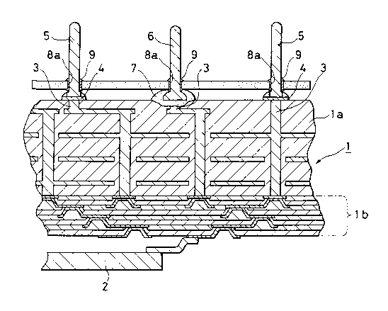
FIG. 6 shows a construction of a multilayer circuit
board with a repaired I/O pin for a case when an I/O pin
of I/O pins 5 formed on the rear surface of the ceramic
substrate 1a has broken together with the attachment pad
4, or when it has broken together with a part of the
ceramic substrate 1a.
In the location of the broken I/O pin, a new I/O
pin 6 (repair pin, or pin for repairing the broken
location) is secured to the rear surface of the
ceramic substrate 1a using an electrically conductive
adhesive 7. Also, the repair pin 6 is bridged to the
surrounding I/O pins 5 using a fixation plate 8 with
holes 8a in which the pins 5 and 6 are placed erect, and
each of the I/O pins 5 and 6 are supported by securing
them to the fixation plate 8 using adhesive 9.
The embodiment of the repairing process according to
2080094
-
this invention will be explaiend in more detail with
reference to FIG. 7 through FIG. 9.
First, as shown in FIG. 7, the conductive adhesive 7
is filled in where the broken I/O pin was located, and the
repair pin 6 is placed erect in this conductive adhesive
7 and is adhered to the location. At this time, the
location where the repair pin 6 is to be placed erect is
deduced from the measured dimensions from the surrounding
I/O pins 5 to the location. The conductive adhesive 7
used to adhere the repair pin 6 is made of, for instance,
gold-polyimide, silver-epoxy or the like. By adhering
the repair pin 6 to the location of the broken I/O pin
using the conductive adhesive 7, it is possible to repair
the multilayer circuit board 1.
However, by only adhering the repair pin 6 to the
ceramic substrate 1a using conductive adhesive 7, it is
difficult to solidly secure the repair pin 6 to the
ceramic substrate 1a.
Therefore, as shown in the oblique view of FIG. 8,
the repair pin 6 is bridged to the surrounding
I/O pins 5 joined to the ceramic substrate 1a using a
fixation plate 8, and the I/O pins 5 and the repair pin 6
are adhered to the fixation plate 8 using an adhesive 9
and thus the repair pin 6 is supported by the surrounding
I/O pins 5 by way of the fixation plate 8.
In this embodiment of the invention, the fixation
plate 8 is a 0.635 mm thick ceramic plate, and there are
nine holes 8a with a diameter of 0.4 mm formed in this
2080094
fixation plate 8 having the same pitch as the surrounding
I/O pins 5 and the new pin 6. The diameter of these
holes 8a is regulated by the precision of the location
when placing the repair pin 6 erect, however, it is
desired that it is about 0.1 mm larger than the diameter
of the surrounding I/O pins 5 and the repair pin 6.
Also, it is possible to use a type of epoxy or a
type of ceramics as the adhesive 9, and it is desired that
this adhesive 9 be filled in between each of the pins 5
and 6 and each of the holes 8a.
FIG. 9 is a cross-sectional view taken along a line
A-A of FIG. 8. As shown in the figure, the adhesive 9
is filled in between each of the holes 8a formed in the
fixation plate 8 and each of the surrounding I/O pins 5
and repair pin 6, and the fixation plate 8 is placed at
the base of each pin 5, 6. By placing the fixation plate
8 at or near the base of each pin 5, 6, it is possible to
make sure that the pins 5 and 6 are solidly secured.
Referring now to FIG. 10, the adhesive 9 is
completely filled in between each of the holes 8a formed
in the fixation plate 8a and each of the surrounding I/O
pins 5 and repair pin 6 and in a space between the rear
surface of the ceramic substrate 1a and the fixation
plate 8, the space including the header portion of the
surrounding I/O pins 5 and repair pin 6, and the pins are
adhered to the fixation plate 8.
In this case, in order that migration of adjacent
pins 5, 6 does not occur inside the adhesive 9, it is
2080094
desired that an adhesive 9 be selected which is superior
in migration resistance.
FIG. 11 is a cross-sectional view of a construction
of a multilayer circuit board with a repaired pin
wherein, together with forming nine holes 1Oa having the
same pitch as the surrounding I/O pins 5 and the repair
pin 6, concave sections 1Ob are formed in a fixation
plate 10 in locations corresponding to the header section
of the pins 5 and 6.
The material and thickness of the fixation plate 10
are the same as those of the fixation plate 8 of the
embodiments mentioned above.
In this case, it is possible for the fixation plate
10 to come in approximately or satisfactorily direct
contact with the rear surface of the ceramic substrate
1a, making it possible for the pins 5 and 6 to protrude
further out from the fixation plate 10, i.e. pin
extension out of the fixation plate 10 being able to
become longer.
FIG. 12 is a cross-sectional view of a construction
of a multilayer circuit board with a repaired pin
wherein, together with forming nine holes 11a having the
same pitch as the surrounding I/O pins 5 and the repair
pin 6, projections (e.g. boss) 11b are formed around the
holes 1la, respectively, in a fixation plate 11.
The material and thickness of the fixation plate 11
are the same as those of the fixation plates 8 and 10
mentioned above.
2080094
In this case, it is possible to lengthen the contact
length of the pins 5, 6 with the fixation plate 11, i.e.
the holes 11a, making it possible to more solidly secure
the repair pin 6.
In each of the aforementioned embodiments, a ceramic
plate was used as the fixation plates 8, 10 and 11,
however, the plate is not limited to this material. It
is also possible to use other materials which have
superior electrical insulating properties, which are
strong, and which are superior in thermal resistance.
Also, the number of holes 8a, 10a, 11a formed in the
fixation plates 8, 10, 11 is not limited to nine; any
number can be selected as long as the repair pin is
solidly supported.
Recently, in view of an aspect of electrical
characteristics, a substrate of low strength such as a
glass ceramics substrate must be often selected for a
multilayer circuit board and thus, when an I/O pin or
pins breaks, a part of the substrate often breaks or is
tore out together with the pin. In such a case, a
process for repairing the broken I/O pin or pins
according to this invention is very important.
As described above, this invention makes it possible
to repair a multilayer circuit board with a ceramics or
glass ceramics substrate when I/O pins used for external
connection of the multilayer circuit board break, even if
this breakage causes a part of the substrate to break off
as well. Therefore, it is not necessary to replace the
- 10 -
2080094
expensive multilayer circuit board but rather electronic
devices can be repaired.
While this invention has been particularly described
with reference to the preferred embodiments thereof, it
will be understood by those skilled in the art that the
foregoing and other changes in form and details may be
made therein without departing from the spirit and scope
of the invention.