Language selection

Search

Patent 2080299 Summary

Third-party information liability

Some of the information on this Web page has been provided by external sources. The Government of Canada is not responsible for the accuracy, reliability or currency of the information supplied by external sources. Users wishing to rely upon this information should consult directly with the source of the information. Content provided by external sources is not subject to official languages, privacy and accessibility requirements.

Claims and Abstract availability

Any discrepancies in the text and image of the Claims and Abstract are due to differing posting times. Text of the Claims and Abstract are posted:

  • At the time the application is open to public inspection;
  • At the time of issue of the patent (grant).
(12) Patent: (11) CA 2080299
(54) English Title: DATA SECURITY ARRANGEMENT FOR SEMICONDUCTOR PROGRAMMABLE LOGIC DEVICES
(54) French Title: DISPOSITIF DE PROTECTION DE DONNEES POUR CIRCUITS LOGIQUES PROGRAMMABLES A SEMICONDUCTEUR
Status: Expired and beyond the Period of Reversal
Bibliographic Data
(51) International Patent Classification (IPC):
  • H04L 09/06 (2006.01)
  • G06F 01/00 (2006.01)
  • G11C 07/24 (2006.01)
  • G11C 16/22 (2006.01)
(72) Inventors :
  • AUSTIN, KENNETH (United Kingdom)
(73) Owners :
  • MOTOROLA INC.
  • PILKINGTON MICRO-ELECTRONICS LIMITED
(71) Applicants :
  • MOTOROLA INC. (United States of America)
  • PILKINGTON MICRO-ELECTRONICS LIMITED (United Kingdom)
(74) Agent: FINLAYSON & SINGLEHURST
(74) Associate agent:
(45) Issued: 2002-12-24
(22) Filed Date: 1992-10-09
(41) Open to Public Inspection: 1993-04-12
Examination requested: 1999-08-16
Availability of licence: N/A
Dedicated to the Public: N/A
(25) Language of filing: English

Patent Cooperation Treaty (PCT): No

(30) Application Priority Data:
Application No. Country/Territory Date
9121591.3 (United Kingdom) 1991-10-11

Abstracts

English Abstract


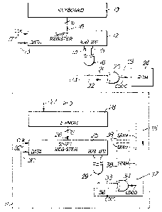
A data security arrangement is provided to protect
configuration data CDI to be stored in static random access
memories SRAM in semiconductor programmable logic devices
PLD. The configuration data, which is vulnerable to illegal
duplication, is normally held in a read only memory ROM,
typically an erasable programmable read only memory. A
data coding means is provided to code the configuration
data to be loaded to the PLD and a data decoding means is
provided in the PLD to decode the coded configuration data.
The coding and decoding means each incorporate maximal length
shift registers which generate a pseudo-random sequence of
bits. A key value is input to the shift register in the
coding means forcing it to start at a particular point in the
sequence. The output (bits B28 and B31) of this register is
combined in an EXCLUSIVE-OR gate with configuration data and
coded data is written to the read only memory ROM. The
decoding means in the PLD has a corresponding key value held
in a non-volatile memory in the PLD. This is applied to the
register of the decoding means, whose output (bits B28 and
B31) are combined in an EXCLUSIVE-OR gate with coded
configuration data CDIC read from the ROM to produce decoded
configuration data CDOD to be stored in the memories.


Claims

Note: Claims are shown in the official language in which they were submitted.


-6-
WHAT IS CLAIMED IS:
1. A data security arrangement for a semiconductor
programmable logic device comprising in combination;
a data coding means arranged to code originating
operating data provided to program the programmable
logic device;
first storage means for storing coded originating
operating data;
data decoding means incorporated in the programmable
logic device for decoding coded originating operating
data: and,
second storage means incorporated in the programmable
logic device for storing decoded originating data;
wherein the originating operating data is coded by the data
coding device and is loaded to the first storage means for
storage therein, and wherein the stored coded originating
operating data is capable of being read from the first storage
means and decoded by the decoding means into the originating
operating data form and loaded to the second storage means for
storage therein.
2. A data security arrangement as claimed in claim 1,
wherein the data coding means and the data decoding means each
include a pseudo-random sequence generator.
3. A data security arrangement as claimed in claim 2,
wherein the pseudo-random sequence generator is constituted by
a 31-bit maximal length shift register which generates a
pseudo-random sequence equivalent to 2,147,483,647 bits in
overall length.

-7-
4. A data security arrangement as claimed in claim 3,
wherein the maximal length shift register has a preload input
and a DATA input.
5. A data security arrangement as claimed in claim 4,
wherein bit 28 and bit 31 outputs of the maximal length shift
register are input to an EXCLUSIVE-OR logic function whose
output is connected to the DATA input of the maximal length
shift register.
6. A data security arrangement as claimed in claim 4,
wherein the maximal length shift register is forced to start
the pseudo-random sequence at a particular point in the
sequence by the application of a predetermined sequence start
code constituted by a 31-bit "key value" to the preload input.
7. A data security arrangement as claimed in claim 6,
wherein the application of the sequence start code to the
maximal length shift register in the data coding means is
input from a keyboard or from a secure file.
8. A data security arrangement as claimed in claim 6,
wherein the application of the sequence start code to the
maximal shift register in the data decoding means is input
from a non-volatile memory within the programmable logic
device.
9. A data security arrangement as claimed in claim 3,
wherein the originating operating data is circuit
configuration data and wherein in the data coding means the
circuit configuration data and the pseudo-random sequence are
input to an EXCLUSIVE-OR logic function which outputs coded
circuit configuration data.

-8-
10. A data security arrangement as claimed in claim 9,
wherein the pseudo-random sequence and the coded circuit
configuration data are input to an EXCLUSIVE-OR logic function
in the data decoding means to provide an output of decoded
circuit configuration data.
11. A data security arrangement as claimed in claim 1,
wherein the first storage means is constituted by a read only
memory.
12. A data security arrangement as claimed in claim 1,
wherein the associated second storage means is constituted by
static random access memories.

Description

Note: Descriptions are shown in the official language in which they were submitted.


_ 1 _
DATA SECURITY ARRANGEMENT FOR
SEMICONDUCTOR PROGRAMMABLE LOGIC DEVICES
BACKGROUND OF THE INVENTION
The present invention relates to data security
arrangements for semiconductor programmable logic devices.
The invention finds particular utility in
semiconductor programmable logic devices (PLDs) of the type
including an associated storage means e.g. a static random
access memory (SRAM) in which circuit configuration data,
necessary for the device to operate, is retained.
It is well known that prior to a PLD being loaded
with appropriate circuit configuration data, such data is
normally held in an external storage medium e.g. an erasable
programmable read only memory (EPROM). A disadvantage of
the present circuit configuration data loading arrangements
to the PLD is that a copy can be readily taken and as a
consequence valuable and sensitive circuit information can
be easily and illegally duplicated. It is extremely
desirable, therefore, to protect circuit information from
being copied.
An aim of this invention is to overcome this
disadvantage by the provision of a data security arrangement
for loading configuration data which prevents illegal
duplication of such circuit information.
SUMMARY OF THE INVENTION
According to the present invention, there is
provided a data security arrangement for a semiconductor
programmable logic device comprising data coding means,
first storage means, and incorporated within the
programmable logic device, data decoding means together with
associated second storage means, wherein the data coding
means codes originating operating data, and the first
storage means stores the coded originating operating data
and wherein the data decoding means decodes the coded

- 2 -
originating operating data read from the first storage means
into the originating operating data form prior to loading to
the associated second storage means.
Preferably the data coding means and the data decoding
means each include a pseudo-random sequence generator
constituted by a 31-bit maximal length shift register having a
preload input and a DATA input, the shift register generating
a pseudo-random sequence equivalent to 2.,147,483,647 bits in
overall length.
Preferably bit 28 and bit 31 outputs of the maximal
length shift register are input to an EXCLUSIVE-OR logic
function whose output is connected to the DATA input of the
maximal length shift register.
The maximal length shift register is preferably forced to
start the pseudo-random sequence at a particular point in the
sequence by the application of a predetermined sequence start
code constituted by a 31-bit "key value" to the preload input.
The application of the sequence start code to the maximal
length shift register in the data coding means may be input
from a keyboard or from a secure file, whereas the application
of the sequence start node to the maximal shift register in
the data decoding means is preferably input from a
non-volatile memory within the programmable logic device.
The data employed to enable the programmable logic device
to operate is preferably circuit configuration data and it is
arranged in the data coding means for the circuit
configuration data and the pseudo-random sequence to be input
to an EXCLUSIVE-OR logic function to provide an output of
coded circuit configuration data.
Preferably in the data decoding means the pseudo-random
sequence and the coded circuit configuration data are input to
an EXCLUSIVE-OR logic function to provide an output of decoded
circuit configuration data.
The first storage means may be constituted by a read only
memory, whereas the associated second storage means is

- 3 -
constituted by static random access memories.
The invention will be more readily understood from the
following description of an exemplary embodiment which should
be read in conjunction with the accompanying drawing.
BRIEF DESCRIPTION OF THE DRAWINGS
The drawing illustrates a block schematic circuit diagram
of the data security arrangements in accordance with this
invention.
DESCRIPTION OF THE PREFERRED EMBODIMENT
Referring to the drawing, a programmable logic device 11
is represented by the block designated PLD. To facilitate
security of data loaded to the PLD, a data coding means is
provided to code circuit configuration data, termed
originating operating data, which is to be loaded to the PLD,
and similarly a corresponding data decoding means is provided
in the PLD to decode the coded circuit configuration data in
the PLD.
Referring to the data coding means in more detail, a
particular form of shift register 12 is provided which
generates a maximal length pseudo-random output string. This
type of shift register is known as a "maximal length shift
register" and in the present application the overall length of
the pseudo-random sequence is arranged to be equivalent to
2,147,483,647 bits (see CMOS COOK BOOK by Don Lancaster pages
318-323, published by Howard W Sams Corp 1980).
This is achieved by feeding back to a DATA input 13 of
the register, particular outputs 14 and 15 of the register in
a particular manner. In this instance both outputs 14, 15
which provide bits B28 and B31 are input to an EXCLUSIVE-OR
gate 16 and the output of this gate is input to the DATA input
13. Providing the register 12 is continuously driven by a

- 4 -
clock input signal 17, the generated pseudo-random sequence is
continuously repeated.
In the data coding means the register 12 is preloaded (in
parallel form) with a predetermined one of different "key
values", each of 31 bits, typically input to a preload input
18 by way of a keyboard 19 or alternatively from a secure
file. The "key value" oahich may be termed a sequence start
code, forces the shift register 12 to start the pseuda-random
sequence at a particular point in the sequence and thereby
recreate an identical sequence at any time as required.
The pseudo-random sequence output from the EXCLUSIVE-OR
gate 16 is input at 21 to a further EXCLUSTVE-OR gate 20.
Circuit configuration data CDI (generated from circuit
configuration layout software) which is to be coded is input
at 22 to the gate 20. The output 23 from the EXCLUSIVE-OR
gate 20 generates coded circuit configuration data CDOC.
The coded circuit configuration data CDOC is output from
gate 20 to a first storage means 24, typically, a read only
memory, where.it is held until required by the programmable
logic device 11. The circuit configuration data now stored in
the first storage medium 24 is coded and secure, and if copied
in this form would not yield any useful circuit information to
the data copier.
To make use of the circuit configuration data in the
programmable logic device 11 when it is read from the first
storage medium 24, the data needs to be reproduced in its
original form and this is achieved by data decoding means.
The data decoding means is required to regenerate the
same pseudo-random sequence of bits as was employed in the
data coding means. Accordingly, the programmable logic device
11 incorporates a 31-bit maximal length shift register 25 of
the same form as the register 12 employed in the data coding
means.
For decoding to be accurate and effective the shift
register 25 must commence its pseudo-random sequence at the

-- 5 -
corresponding point at which the shift register 12 commenced
its sequence. Accordingly the identical predetermined 31-bit
"key-value" or sequence start code which was used to start
register 12 must be applied, in parallel form, to a preload
input 26 of the register 25 to force it to start its sequence
at the same point in the sequence as register 12, and thereby
generate an identical pseudo-random sequence.
The required 31-bit "key value" is input at 27 and stored
in a form of non-volatile memory on the PLD 11, for example,
an EPROM 28 or fusible links.
The shift register 25 operates in a manner similar to
shift register 12, the output bits B28 and B31 being input to
an EXCLUSIVE-OR gate 29 whose output is fed to.the DATA input
30 of the register. The register 25 is driven by the clock
signal CLK input at 32,
The pseudo-random sequence output from EXCLUSIVE-OR gate
29 forms an input 33 to a further EXCLUSIVE-OR gate 34 and
coded circuit configuration data CDIC which is output from the
first storage means 24 on line 35 forms a second input 36 to
the gate 34.
The EXCLUSIVE°OR function of the gate 34 upon its two
signal-inputs produces an output 37, in serial form, of the
originating operating data (the circuit configuration data).
This originating operating data is now available for use
within the programmable logic device PLD, for instance,
loading into associated second storage means in the form of
static random access memories SRAM 38.

Representative Drawing
A single figure which represents the drawing illustrating the invention.
Administrative Status

2024-08-01:As part of the Next Generation Patents (NGP) transition, the Canadian Patents Database (CPD) now contains a more detailed Event History, which replicates the Event Log of our new back-office solution.

Please note that "Inactive:" events refers to events no longer in use in our new back-office solution.

For a clearer understanding of the status of the application/patent presented on this page, the site Disclaimer , as well as the definitions for Patent , Event History , Maintenance Fee  and Payment History  should be consulted.

Event History

Description Date
Inactive: IPC expired 2013-01-01
Time Limit for Reversal Expired 2009-10-09
Letter Sent 2008-10-09
Inactive: IPC from MCD 2006-03-11
Grant by Issuance 2002-12-24
Inactive: Cover page published 2002-12-23
Pre-grant 2002-10-09
Inactive: Final fee received 2002-10-09
Notice of Allowance is Issued 2002-04-09
Letter Sent 2002-04-09
Notice of Allowance is Issued 2002-04-09
Inactive: Approved for allowance (AFA) 2002-03-28
Amendment Received - Voluntary Amendment 2000-02-01
Inactive: Office letter 1999-12-10
Letter Sent 1999-12-10
Inactive: Multiple transfers 1999-11-02
Inactive: Application prosecuted on TS as of Log entry date 1999-09-15
Letter Sent 1999-09-15
Inactive: Status info is complete as of Log entry date 1999-09-15
All Requirements for Examination Determined Compliant 1999-08-16
Request for Examination Requirements Determined Compliant 1999-08-16
Letter Sent 1998-12-18
Reinstatement Requirements Deemed Compliant for All Abandonment Reasons 1998-12-09
Deemed Abandoned - Failure to Respond to Maintenance Fee Notice 1998-10-09
Letter Sent 1998-04-15
Reinstatement Requirements Deemed Compliant for All Abandonment Reasons 1998-04-07
Deemed Abandoned - Failure to Respond to Maintenance Fee Notice 1997-10-09
Application Published (Open to Public Inspection) 1993-04-12

Abandonment History

Abandonment Date Reason Reinstatement Date
1998-10-09
1997-10-09

Maintenance Fee

The last payment was received on 2002-09-23

Note : If the full payment has not been received on or before the date indicated, a further fee may be required which may be one of the following

  • the reinstatement fee;
  • the late payment fee; or
  • additional fee to reverse deemed expiry.

Patent fees are adjusted on the 1st of January every year. The amounts above are the current amounts if received by December 31 of the current year.
Please refer to the CIPO Patent Fees web page to see all current fee amounts.

Owners on Record

Note: Records showing the ownership history in alphabetical order.

Current Owners on Record
MOTOROLA INC.
PILKINGTON MICRO-ELECTRONICS LIMITED
Past Owners on Record
KENNETH AUSTIN
Past Owners that do not appear in the "Owners on Record" listing will appear in other documentation within the application.
Documents

To view selected files, please enter reCAPTCHA code :


To view images, click a link in the Document Description column. To download the documents, select one or more checkboxes in the first column and then click the "Download Selected in PDF format (Zip Archive)" or the "Download Selected as Single PDF" button.

List of published and non-published patent-specific documents on the CPD .

If you have any difficulty accessing content, you can call the Client Service Centre at 1-866-997-1936 or send them an e-mail at CIPO Client Service Centre.


Document
Description 
Date
(yyyy-mm-dd) 
Number of pages   Size of Image (KB) 
Representative drawing 2002-03-27 1 10
Claims 1993-12-17 3 75
Abstract 1993-12-17 1 31
Drawings 1993-12-17 1 21
Description 1993-12-17 5 195
Representative drawing 1998-10-25 1 17
Courtesy - Abandonment Letter (Maintenance Fee) 1997-11-05 1 186
Notice of Reinstatement 1998-04-14 1 170
Courtesy - Abandonment Letter (Maintenance Fee) 1998-11-08 1 184
Notice of Reinstatement 1998-12-17 1 170
Reminder - Request for Examination 1999-06-09 1 118
Acknowledgement of Request for Examination 1999-09-14 1 193
Commissioner's Notice - Application Found Allowable 2002-04-08 1 166
Maintenance Fee Notice 2008-11-19 1 172
Correspondence 2002-10-08 1 36
Correspondence 1999-12-09 1 8
Fees 1998-12-08 1 40
Fees 1998-04-06 1 45
Fees 1994-11-16 6 362
Fees 1996-09-29 1 50
Fees 1995-10-05 1 31
Fees 1994-11-02 1 47