Note: Descriptions are shown in the official language in which they were submitted.
~~~~~~J
FIELD OF THE TNVENTTON
The invention described herein is a device for generating
wide band pulses of radio frequency energy.
BACKGROUND OF THE TNVENTION
Recently, considerable progress has been made in the
generation of high power pulses for applicat:ian to a wide-band
impulse transmitter by charging up the semiconductor material of a
transmission line and discharging it by rendering the material at
an end of the line conductive with a pulsed laser beam. This
causes a travelling wave to flow to that end of the line 'that can
be coupled to an antenna. Thus the semiconductor material stores
the energy and acts as a switch. Coaxial and microstrip lines have
been used, but radial transmission lines praduce pulses of higher
voltage because the travelling waves converge at its center.
A radial transmission line device and a system for using
it tc generate radio frequency pulses in response to pulses of
laser light is described in an article entitled "Monolithic,
photoconductive impulse generator using a GaAs wafer" that was
authored by people including the inventors of this invention and
which appeared in the dune 17, 2991 issue of "Applied Physics
Letters 58 (24)".
One of the problems encountered with that device is the
inefficient manner with which the optical energy from laser diodes
made of GaAs material is transferred to the wafer disk of GaAs.
This means that a larger array of laser diodes must be used in
order to transfer a required amount of optical energy to the disk.
The resulting increase in the threshold current for driving the
array increases the rise time of the laser pulses thereby limiting
the range of RF frequencies 'that can be produced. The increase in
threshold current also reduces the laser pulse repetition frequency
so as to reduce the RF output power that may be attained.
Furthermore, the thermal and mechanical stability of the
known device is such as to reduce its life when high bias voltage
and a high pulse repetition frequency are employed to increase its
output power.
SUMMARY OF THE INVENTION
Instead of making the ohmic contacts between a substrate
of semiconductor material made of GaAs and the metal layers on its
top and bottom surfaces by doping the top and bottom surfaces in
the required areas with n or p type material, the ohmic bonding is
achieved by forming n or p type epitaxial layers of GaAs between
the substrate and the metal layers. This increases the thermal and
mechanical stability so as to increase the life of the device.
In accordance with another aspect of this invention, an
optical window in the form of an AIGaAs epitaxial layer is formed
on the substrate in the central area where the laser light enters
it. Because the AlGaAs layer has a band gap energy from 1.42 to
2.16 electron volts and the GaAs used in the laser diodes has a
typical band gap energy of 1.43 electron volts, the AlGaAs layer is
transparent to the laser pulses and thereby increases the
efficiency with which they enter the substrate.
- 2 -
2~8~~~~
BRTEF DESCRIPTION OF THE DRAWINGS
The invention is described in detail below with reference
to the drawings, in which like items are indicated by the same
reference designation, wherein:
Figure 1 shows a transverse diametric cross sectianal
view of a known device for generating radio frequency pulses arzd
required operating components;
Figure 2 is a top view of the device having a diametric
cross section as depicted in Figure 1;
Figure 3 is a bottom view of the device depicted in
Figure 1;
Figure 4 is a transverse diametric cross sectional view
taken along 4~4 of Figure 5 of a wafer type RF pulse generating
device of this invention having laser light entering from the top;
Figure 5 is a top view of the wafer type RF pulse
generating device of this invention shown in Figure 4;
Figure 6 is a bottom view of the caafer type RF pulse
generating device of this invention as depicted in Figure ~;
Figure 7 is a transverse diametric crass section of wafer
type RF pulse generating device of this invention having laser
light entering from both the top and bottom faces thereof;
Figure 8 is a top view of a wafer type RF pulse
generating device as depicted in Figure 7;
Figure 9 is a bottom view of a wafer type RF pulse
generating device as depicted in Figure 7.
Figure 10 is a block diagram for an RF pulse generating
system utilizing a wafer type device depicted in Figures 7-9;
~~8~~33
Figure 11 is a graph illustrating the charging
characteristics of a wafer type RF pulse generating device of this
invention;
Figure 12 is a graphical illustration of a laser pulse
for triggering RF pulse generating wafer type devices of this
invention as well as laser pulses for triggering known wafer type
devices; and
Figure 13 is a graphical illustration of an output pulse
provided by a system using the wafer 'type pulse generating device
of this invention as well as an output pulse produced by a system
using a known wafer type device.
DETAILED DESCRIPTION
Various aspects of the system described in "Applied
Physics Letters 58(24) are shown in Figures 1,2 and 3 wherein a
disk 2 of semiconductor material such as GaAs has an annular metal
layer 4 ohmically bonded to one surface 5 by n or p doped region 6
of the disk 2 and an annular metal layer 8 ohmically bonded to the
other surface 9 by an n or p doped region 10. The central openings
of the annular metal layer 4 and the underlying doped region 6 are
respectively indicated as 12 and 14. An inner conductor 16 of a
coaxial line 18 is ohmically bonded to the center of the opening 20
in the annular layer 8 by an n or p type doped region 22. The
outer conductor 24 of the coaxial line 18 is ohmically adhered to
the annular metal layer 8 by soldering or the like as indicated at
26.
Generation of RF pulses is achieved by connecting a
source 28 of DC charging pulses between the metal layers 8 and 4
_ 4 _
~~8~4~~
and directing much shorter trigger pulses of laser light from a
source 30 through the openings 12 and 14. rn a matter of
nanoseconds, the laser light renders the central portion of the
wafer 2 conductive so that the capacitor formed by the disk 2 and
the metal layers 4 and 8 is discharged through a load impedance 32
that is connected between the inner and outer conductors 16 and 24
of the coaxial line 18. This causes RF waves to travel inwardly to
the center of the wafer and along the transmission line 18. The
load 32 is typically a remotely located antenna.
Figures 4, 5 and 6 are respectively a diametric cross
section, top and bottom views of a wafer type RF pulse generating
device of this invention wherein trigger pulses of laser light
enter from one side. A wafer, which may in this example be in the
form of disk 34 of semiconductor material such as GaAs, preferably
has an annular n type epitaxial annular layer 36 formed on one side
(top) thereof and a p type annular layer 38 formed on the other
side (bottom) thereof, but the epitaxial layers 36 and 38 may be of
n or p types that are the same or different.
In accordance with one aspect of this invention, an
optical window is formed by an AlGaAs epitaxial layer 40 on the top
face of disk 34 within the center of the annular epitaxial layer 36
and separated therefrom as indicated at 37. The outer surface of
the annulax epitaxial layer 36 is metallized as indicated at 39 to
form an electrode, and the central epitaxial layer 40 is metallized
to form a grid 41 of apertures such as, for example, apertures 42,
44, 46 and 48 shown in Figure 5. Only apertures 42 and 44 appear
in Figure 4. The grid 41 of apertures can have various degrees of
openness. Note that alternatively epitaxial layer 40 can be
5
CA 02080433 1999-12-09
eliminated to leave a centrally located aperture through
metallization layer 39 and epitaxial layer 36 to the disk 34.
With reference to Figures 4 and 6, a p type epitaxial
layer 49 is preferably formed on the bottom face of the disk 34 in
the center thereof and spaced from and concentric with the p type
epitaxial layer 38. The layers 38 and 49 are metallized as
indicated at 50 and 52, respectively. An :inner conductor 54 of a
coaxial cable 56 is soldered or otherwise conductively connected to
the metallized layer 50, and the outer conductor 58 of the coaxial
1o cable 56 is conductively connected to the metallized layer 52. In
order to provide longer leakage paths between the metallized layers
39 and 52, their diameters are less than the diameter of the disk
34.
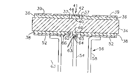
Figures 7, 8 and 9 are respect=ively a diametric cross
section, top and bottom views of a wafer type RF pulse generating
device of this invention wherein trigger pulses of laser light
enter from both th~= top and bottom faces. Those parts of the
device of Figures '7, 8 and 9 that correspond to parts shown in
Figures 4, 5 and 6 are designated by the same numerals.
2o The difference between the device shown in Figures 7, 8
and 9 and the devi~~e shown in Figures 4, 5 and 6 lies in the
provision of means for directing laser light to the center of the
bottom of the disk 34. In this particu7_ar example, an annulus 60
of p type epitaxia:L material is formed about the center of the
bottom face so as i~o be concentric with the annular layer 38 and
spaced from it via a circular channel 66. The annulus 60 is
metallized as indicated at 62, and a cavity 64 is formed in the end
of the inner conductor 54. The annular end of the inner conductor
- 6 -
CA 02080433 1999-12-09
54 is conductively attached to the metallized annulus 62. Pulses
of laser light are conducted to the epitaxial layer 60 by a fiber
optic bundle 63 that extends through a wall of the cavity 64 into
aperture 65. The metallization 62 has a through hole 65 for
receiving fiber optic 63 to permit the light to pass to AlGaAs
epitaxial layer 60, to disk or substrata 34. Thus, the trigger
pulses of laser light can enter the disk 34 of semiconductor
material from both the top and bottom faces, as well as only the
top or bottom face. Using both faces for receiving trigger pulses
1o reduces the time required to reorder the center of the disk 34
conductive with a given array of laser diodes.
Reference is now made to the block diagram of Figure 10
illustrating an RF pulsing system utilizing the wafer type device
of Figures 7, 8 and 9. In this figure, the wafer device is
generally shown in the same way as in F_~gure 7.
A master pulse generator 68, which may be a Hewlett
Packard Model 214B (manufactured by Hewlett-Packard, Palo Alto, CA)
supplies a trigger pulse via an output 70 to a high voltage
charging pulser 72. The output 74 of a high voltage charging
2o pulser 72 (50 to 75 KV, 5.0 U.S. charge time, manufactured by
Signum Electronics, for example) is connected to the metallized
electrode 39 of thEy wafer device 76, and the metallized surface 52
is connected to a potential to which all_ of the circuits are
referenced in a manner not shown.
An output= 78 of the master pu7_se generator 68 is
connected to a trigger input 80 of a pulse generator 82 that may
also be a Hewlett 1?ackard Model 214B, for example. The generator
82 provides a suitably delayed pulse at an output 84 that is
_ 7 _
CA 02080433 1999-12-09
coupled to an input 86 of a laser diode driver 88 (Model AVO-P,
manufactured by AV Tech Electrosystems, Ltd., Ottawa, Canada, for
example). The driver 88 derives its operating potential from a low
voltage power supply 90. An array 92 of laser diodes (LDT 350 LED
Array, manufactured by Laser Diode Corp., New Brunswick, NJ, for
example) is coupled to the driver 88, and laser light is coupled by
a bundle 94 of optical fibers to the grid 41 having apertures 42,
44, 46 and 48 therein and by the bundle 63 (see Figure 7) of
optical fibers to the AlGaAs epitaxial layer 60.
Operation of the system of Figure 10 is now explained by
reference to the graphs of Figures 11, 12 and 13. The time scales
represented by the abscissa of these figures are different. The
time scale for Figure 11 is in hundreds of microseconds, and
although the time scales for Figures 12 and 13 are in nanoseconds,
the time scale for Figure 13 is much expanded in respect to the
time scale for Figure 12. The graph of Figure 11 shows the buildup
of voltage between the metallized layers 39 and 52 following
application of a high voltage pulse from the output 74 of the high
voltage charging pulser 72. As can be seen, it takes a time t for
2o the voltage to build up to a maximum value V~.
Because ~~f delay provided by t=he pulse generator 82, a
pulse at its output 84 starts at the time t. and causes the pulse of
laser light produced by the diode array 92 to be as indicated at 96
of Figure 12. The pulse 96 preferably has a width that is less
than 40 ns. This :is much shorter than t:he duration of the charging
pulses at the output 74 of the pulser 72. The electrical output
pulse 98 of Figure 13 is preferably 2-4 ns, which is less in
_ g -
CA 02080433 1999-12-09
duration than the laser pulse 96 of Figure 12, but pulse 98 appears
to be longer because of the time scale.
In order to produce as wide a range of radio frequencies
as possible, the duration of the output pulse 98 should be as short
as possible. This depends on the rate at which laser light energy
is imparted to the semiconductor disk 34, and this in turn depends
on the rise time of the triggering laser pulse 96. Thus, if the
laser pulse had a slower rise time as indicated by the dashed curve
96' of Figure 12, the output pulse would have a longer duration as
1o indicated by the dashed line 98'. Because of the more efficient
optical coupling of the epitaxial layers 40 and 60, the rate at
which laser light is introduced to the disk 34 is increased for any
given number of diodes in the array 92. As previously noted,
increasing the number of diodes so as to increase the intensity of
the laser light would also increase the required threshold current
and slow down the rate of rise of the laser_ pulse.
Furthermore, the rapidity with which the semiconductor
material at the ce:zter of the disk 34 can be made conductive is
increased by subje~~ting it to laser light from both sides, thereby
2o creating a more uniform carrier distribution throughout the
semiconductor, and thereby leading to a sudden collapse of the
electric field in -the semiconductor.
Preferab:Ly, more than the four apertures 42, 44, 46 and
48 would be provided in the grid 41. The reason why having more
than one aperture :is beneficial is because a more uniform
electrical field i:~ established along the axis of the semiconductor
disk 34.
_ g
~~~~~~J
Because the device is subjected to severe operating
conditions such as high bias voltage such as -t-Vp (see Figure 10) and
a high pulse rate frequency, its thermal and mechanical stability
has been enhanced through use of 'the epitaxial layers 36 and 3~
were not used to provide the ohmic bonding of the grid 41 and the
metallized layers 30, 50 and 52.
Although various embodiments of the invention have been
described and shown herein, they are not meant to be limiting.
Those of skill in the art may recognize certain modifications to
these embodiments, which modifications are meant to be covered by
the spirit and scope of the appended claims. For example,
materials other than GaAs and AlGaAs can be used. Also, the shape
of the present device can be any practical shape not limited to a
disk shape, such as square, rectangular, and so forth.
- 10 -