Note: Descriptions are shown in the official language in which they were submitted.
WO 91!17515 P~'1'/US90/04577
Descr~tion
Diaanostic hardware for Serial Datalink
Technical Field
This invention relates generally to a
bidirectianal communications network having a ring
configuration, and more specifically, to an apparatus
for providing fault and noise tolerance capabilities
to a serial communications datalink.
Backaround Art
With the use of intelligent control modules
on a vehicle (for example, microprocessor-based
controllers), a system which provides cost effective
and reliable serial communications between such
intelligent modules h'as become increasingly important.
There are four basic types of communication
networks: the serial bus network, the bus ring
network, the general ring network and the
bidirectional ring network. In a serial bus network,
the modules are connected through a transmission line
(or bus). Each module has a transmitter for putting
data onto the bus and a receiver for reading data off
of the bus. Fig. 1 shows a typical bus network 100.
Each module 102,104,106 is connected to a bus 108. In
the bus ring nevtwork 200, as illustrated in Fig. 2
modules 202,204,206 are coranected by a bus 208, as in
the normal bus network 100 described above, but the
bus 208 is in the form of a ring.
In the general ring configuration, as
illtastrated by the ring network 300 of Fig. 3, each
module 302,304,306 is connected to the previous module
and to the next module by a separate transmission
line. Each module contains a receiver 308A,308B,308C
WO 91/1761 FCT/US90/04677
2~~~~.~~ -2w
for receiving data from the previous module and a
transmitter 310A,310B,310C for transmitting data to
the next module in the ring. This configuration
provides unidirectional communication around the ring.
As illustrated in Fig.4, each module 402,404,406 in
the bidirectional ring network 400 includes two
transmitter/receiver pairs
408A,408B,408C,410A,410B,410C. One
transmitter/receiver pair 408A,408B,408C from each
control module 402,404,406 provides communication
around the ring in one direction using one set of
transmission lines. The other transmitter/receiver
pair 410A,410B,410C provides co8ununication in the
other direction around the ring using another set of
transmission lines. Each set of transmission lines
consists of a pair of wires. Data being transmitted
over the transmission lines are.determined by the
voltage differential in the wire pair. This
configuration provides bidirectional communication
around the ring.
Application of a communication network to
intelligent control modules on a vehicle presents
several problems. First, communication may be
hampered by electromotive and electromagnetic
interference. This interference adds noise to the
electrical signals being propagated by the
transmission lines between the control modules making
the data messages indecipherable. The noise may be
seen as an offset bias in the electrical signals being
transmitted over the wire pair. Each wire in 'the pair
would bear the same offset bias. One common method of
determining if a fault has occurred is by comparing
the voltage on the wire pairs in a logic circuit: if
the offset bias becomes large enough (either a large
negative offset bias or a large positive offset bias)
z
-3-
the logic circuit will not be able to differentiate
between the two voltages even though no fault has
occurred. This is known as the common mode problem.
U.S. Patent No. 4,760,571 issued July 26, 1988, to
Siegfried Schwar2, discloses a ring network. The
network includes a noise filter to eliminate
electromotive and electromagnetic interference.
However, at high data rates, filtering of the data can
also affect the integrity of the data messages.
Other solutions for detecting faults require
1) manual access to the transmission lines, 2) the
transmission of special signals, or 3) a system having
a diagnostic mode. All three solutions involve
closing the transmission lines to normal communication
signals. One example of a system using solution 3) is
disclosed in EP-A-239731.
Second, due to space limitations, the
transmission lines are not very accessible. After the
occurrence of a fault in the network (i.e., a short
circuit or open circuit condition on one of the
transmission lines), a manual check of the wiring
harness is difficult and time consuming. It is
therefore desirable to have a network with full
diagnostic capabilities (i.e., giving the location and
the type of fault condition).
Third, if a fault does occur, the faulted
transmission lines) needs to be isolated and the
associated control modules) protected.
Fourth, the common mode problem is to be
3o eliminated without comprising any capabilities of the
system.
The subject invention is directed at
overcoming one or more of the problems as set forth
above.
~U~~ZI'~UT~ ~~~~
t
r
-3/1-
Disclosure of the Invention
In one aspect of the invention, an apparatus
provides fault tolerant serial communications in a
network. The network includes a plurality of control
modules connected on to another. The network
transmits data messages over positive and negative
transmission lines. Each control module has an
15
25
35
$l!'~.,~TIZ'~T~ ~~' ~'~
dV0 91/17615 Pt.'T/US90/04677
1 ~ -4-
associated differential receiver with positive and
negative input terminals and an output terminal. The
negative input terminal is connected to a first
positive receiving wire, the positive input terminal
is connected to a first negative receiving wire, and
'the output terminal is connected to one control
module. The network slam includes a transmitter
associated with each control module. :Each transmitter
includes a first positive line driver connected
between the one control module and a first positive
transmitting wire, and a first negative line driver
connected between the one control module and a first
negative transmitting wire. The network includes
circuits for sensing short circuits between the first
positive receiving wire and ground, sensing short
circuits between the first negative receiving wire and
supply voltage, and for sensing excessive current on
'the first positive and negative transmitting wires.
In another aspect of the present invention,
a method for providing fault tolerant serial
communications in a network is provided. The network
includes a plurality of control modules connected
togethero The network is adapted to transmit data
messages from one control module to another control
module over positive and negative transmission wires.
The method includes the steps of transmitting a data
massage from one control module to another control
module over ones of the fix°st positive and negative
transmission wires, sensing the current flowing
through the first positive and negative transmission
wires as a voltage differential between the positive
and negative transmission wipes, and delivering the
data message to the other control module as a function
of the voltage differential. The method also includes ..
the steps of sensing a short circuit condition between
WO 91/17615 PCi'/IJS90/04677
~5s ~~p~ ~ ~~
the positive transmission wire and ground, sensing a
short circuit condition between the negative
transmission wire and supply voltage, and delivering a
first fault signal in response to either of the~sensed
conditions, sensing the magnitude of current flowing
through the positive transmission wire, comparing the
positive transmission wire current magnitude to a
first reference current value, and delivering a second
fault signal in response to the positi°ve transmission
wire current magnitude being greater than the first
reference current value. The method further includes
the steps of sensing the magnitude of current flowing
through the negative transmission wire, comparing the
negative transmission wire current magnitude to a
second reference current value, and delivering a third
fault signal in response to the negative transmission
wire current magnitude being greater than the second
reference current, and receiving the first, second,
and 'third fault signal and isolating the control
modules from the positive and negative transmission
wires in response to the first, second and third fault
signals.
Brief Description of the Drawings
Fig. 1 is a block diagram of a serial bus
network as known in the prior arty
Fig. 2 is a block diagram o~ a ring bus
network as known in the prior ar°t:
Fig. 3 is a block diagram of a
communications network having control modules
connected in a ring by a transmitter--receiver pair, as
known in the prior art;
Fig. 4 is a block diagram of a redundant
ring network as known in the prior art;
WO 91!17615 PCy'/US90/04677
-
Fig. 5 is a block diagram of a
communications network having a plurality of control
modules in a ring network, each having a pair of
transceivers;
Fig. 6 is a block diagram of one control
module of Fig. having a microprocessor and a logic
board;
Fig. 7 is a functional logic diagram of the
logic module of Fig. 4;
Fig. 8A is a block diagram of the
transceivers of one control module showing a first
embodiment of a pass-through means;
Fig. 8B is a block diagram of the
transceivers of one control module showing a second
embodiment of the pass-through means; and
Fig. 9 is an electrical schematic of the
transceiver and fault diagnostic hardware according to
the present invention.
best Mode fvr Carry~g Out the TnvPntion
With reference to' Fig. 5, the present
invention is adapted to provide communication between
three control modules 502A,502B,502C rnnnected in a
network 500 on a vehicle (not shown). Each control
module 502A,502B,502C has a first transceiver
(transmitter/receiver pair) 504A,504B,504C and a
second transceiver 506A,506B,506C. The control
modules 502A,502B,502C may have varying functions,
which are immaterial to the present invention. The
control modules 502A,502B,502C include logic means
508A,508B,508C which generate and receive data
messages. The data messages generated by one control .
anodule 502A,5028,502C are transmitted to the other
control modules 502A,502B,502C by the first and second
transceivers 504A,506A,504B,506B,504C,506C The
WO 91/17615 PCT/US90/04677
i~ ..~ L
control modules 502A,502B,502C are Connected in a ring
with the first transceiver 504A,504B,504C of each
control module 502A,502B,502C Connected to the second
transceiver 506A,506B,506C of the previous Control
module 502A,502B,502C in the network 500 and the .
second transceiver 506A,506B,506C of each control
module 502A,502B,502G Connected to the first
transceiver 504A,504B,504C of the next Control module
502A,502B,502C in the network 500. A single
LO transmission line 510AB,510BC,510CA connects each
first transceiver 504A,504B,504C to the respective
second transceiver 506A,506B,506C. The transmission
lines 510AB,510BC,510CA, in the preferred embodiment,
are twisted wire pairs.
The data messages are fixed foic~nat serial
bit streams. Each data message begins with a Message
Identification (MID) character: followed by one or
more parameters. Each parameter begins with a
Parameter Identification (PID) character followed by
one or more parameter data Characters. The data
message ends with a checksum character. Each
Character has a start bit, 8 bits of data, and a stop
bit. Alternately, the Mid character Could be replaced .
by a Source Identification (STD) character and a
Destination Identification (DID) character.
With reference to Fig. 6, a fui~Ctional block
diagram of one logic means 508 is shown. The logic
means 508 includes a microprocessor 602 and a logic
board 604. The first and second transceivers 504,506
are shown as separate first and second transmitters
610,611 and first and seCOnd~receivers 612,613. In
the preferred embodiment, the microprocessor 602 as v
adapted to perform a Complex function, for example,
controlling the solenoids of a fuel injection engine.
The microprocessor 602 may receive information from a
~1'O 91/17615 PCTfUS90/04677
~1 ! Vl .i_ .A~
variety of sensors (not shown) to perform its
specified function. The logic board 604 controls the
flow of data messages to and from the microprocessor
602.
With reference to one control module 502,
the transmission line 510 connected to the :First
receiver 612 includes a first positive transmission
wire 606 and a first negative transmission wire 608>
The transmission line 510 connected to i~he second
transceiver 504 includes a second positive
transmission wire 607 and a second negai:ive
transmission wire 609. Logic level °'F1I" is defined ~:o
exist when there is a positive 0.2 voltage
differential between the positive transmission wire
606,607 and the negative transmissian wire 608,609. A
logic level "LO'° is defined to exist when there exists
a negative 0.2 voltage differential between the
positive transmissian wire 606,607 and the negati°ve
transmission wire 608,609. The positive and negative
transmission wires 606,607,608,609 form a pair of
balanced transmission wires,~i.e., the line drivers
and receivers are constructed such that the wires in
each transmission pair have matched impedances. A
second feature of the transmission lines 5~.0 is that
the currents in the posiaive and negative transmission
wires 606,607,608,609 are substantially equal in
magnitude and opposite in direction.
A second convention used is that the idle or
inactive state of the transmission lines 510 is logic
level °°HI°° (the IDLE state). In addition,, the
first
and second transceivers 504,506 are designed such that
a logic °°LO°° signal dominates, i.e., if two
transceivers 504,506 are attempting to transmit on a
transmission line 510 at the same time, the
transmission line 510 always assumes the °°LD°' state
WO 91/17615 PC1'/US90/U4677
D~ ~ Y .i r
IJ
any time either transceiver 504,506 transmits a "LO", w
Logic level "LO" is therefore said to be the DOMINANT
state. In order for one control module 502A,502B,502C
to properly detect the start of data messages
transmitted from another control module
502A,502B,502C, it is therefore necessary that the
first or start bit of each data characaer is a logic
level "LO".
A short circuit detecting mE:ans 622 detects
the presence of short circuit conditions on the
transmission lines 510A13,510BC,510CA. First and
second pinned fault detection means 614,615 associated
with the first and second receivers 612,613,
respectively, sense when the respective transmission
line 510 is shorted in the DOMINANT state, i.e., the
positive transmission wire 606 is shorted to .
electrical ground or the negative transmission wire
608 is shorted to supply voltage.
First and second overcurrent detection means
618,619 protect the control module 502 from large
currents on the positive and negative transmission
wires 606,608,607,609, i.e., the positive transmission
wire 606,607 is.shorted to supply voltage, the
negative transmission wire 608,609 is shorted to
electrical ground, ar the positive and negative
transmission wires 606,608,607,609 are shorted
together. Fault status circuits 621,622 relay the
presence of a pinned fault or overcurrent condition to
the logic board 604.
With reference to Fig. 7, the basic digital
logic circuit 700 found on the logic board 504 is
shown. Serial data to be transmitted is received from
the microprocessor 602 (shaven as signal T~) and passed
to the first and second transmitters 610,611 through
second and third logic gates 720,721. ~'he output of
dV0 91/1765 PCT/U590/04677
mlo-
the first and second receivers 612,613 is relayed to
the microprocessor 602 though a fourth logic gate 7.22
(signal RX).
The logic circuit 700 includes a means 708
for detecting if a data message is present on the
transmission line 510. Signal R.X is connected to a
first logic gate 710 through an inverter 711. The
first logic gate 710 compares the signals RX and TX
and is connected to a flip-flop 712 by a lowpass
filter 714. The lowpass filter 714 includes a
resistor 716 and a capacitor 718. The flip-flop 712
is connected t~ the microprocessor 602 and signals the
microprocessor 602 when a data message from another
control module 502 is being received (signal SBD).
The microprocessor 602 resets the flip-flop 712 by
signal SB~S .
The microprocessor 602 controls the first
and second transceivers 504,506 through the logic
circuit 700 by signals T~, Rte, T~, Rte. Through
these signals, the microprocessor 602 can disable
either transmitter 610,611 (signals T~, T~) and/or
either receiver 612, 613 (R~, Rte) .
When no data messages are being transmitted
or received by any control module 502, both
transmission lines 510 are in the passive or "T3I°'
state, as described above. If a control module 502
needs to transmit a data message, the microprocessor
602 checks signal SBD. The microprocessor 602 delays
transmission of the data message for a period of time
equal to an idle time period. plus a priority time
period after the detecting means ?OS detects the
absence of another data message. Preferably, the idle
time period is equal to the time required to transmit
a character of data, i:e., ten bit times. The
priority time peri~d is different for each module and
WO 91/17615 PCT~U~90 ~04~67~~7'~ '
.... ' '. 2
°11-
prioritizes each module such that, after the
transmission of a data message, no module will attempt
to transmit simultaneously. Then the control module
502 attempts to transmit the data message
simultaneously in both directions through the first
and second transceivers 504,505.
Referring to Figs. 8A and 8B, a data message
received by either the first or second receiver
612,61.3 of one control module 502 is relayed to the
l0 next control module 502 by a pass-through means 802.
In this way, the data message is propagated from
control module 502 to control module 502.
In one embodiment, the pass through means
802 includes a solid state relay 804, as shown in Fig.
8A. Cne suitable relay, part no. Ld31061AB, is
available from AT&T Technologies INC, a subsidiary of
American Telephone & Telegraph C0, located in
Berkeley Hts, New Jersey. The relay 804 is connected
across the control module 502 and is under the control
of the microprocessor 602. The relay 804 is normally
in the closed state, such that the first positive
transmission wire 606 is electrically connected to the '
second positive transmission wire 607. The same is
true for the first and second negative transmission
wires 608,609.
A second embodiment of the pass--through
means 802 is illustrated in Fig. 8B. First and second
pass-through gates 820,822 are connected between the
first and second transceivers 504,506. A noninverting.
input 824 of the first pass-through gate 820 is
connected to the output of the first receiver 612.
The output of the first pass-through gate 820 is
connected to the second transaaitter 611. A
noninverting input 824 of the second pass-through gate
822 is connected to the output of the second receiver
iVO 91/17615 P(_'T/US90/04677
_12_
7f;~' s _~.v
613. The out ut of the second
p pass-through gate 822
is connected to the first transmitter 610. Thus, data
messages received by the first transceiver 504 are
retransmitted to the next control module 502 by the
second transceiver 506. The reverse also holds true.
The first and second pass-through gates
820,822 have first and second inverting inputs 826,828
so that "latch-up" will not occur. "L~itclh-up" is the
situation when the first and second transceivers
504,506 become nonresponsive~ta subsequent signals
after a "LO°' (the DOMINANT state) has been received or
transmitted.
For example, when a "LO°' is received by the
first transceiver 504, the output of the first
receiver 612 and the first pass-through gate 820 both
go '°LO°'. The second transceiver 506 retransmits the
"LO" to the next control module 502. If the second
receiver 613 is allowed to relay the "LO°' back to the
first transmitter 610, the first transmitter 610 will
retransmit the "LO'° and the first receiver 612 will be
nonresponsive when the transmission line 510 attempts
to go ''HI ~' , Ta prevent the retransmitted °'LO°' from
being relayed back to the first transmitter 610, the
output of the first pass-through gate 820 is connected
to the inverting input 826 of the second pass-through
gate 822. The output of the second pass-through gate
822 is "HI", and therefore the first transmitter 610
becomes nonresponsive to the second receiver 613. A
received "~0'° by the second transceiver 506 is handled
in a similar manner and is therefore riot further
discussed.
During transmission of a data message
originating at tl~e control module 502, '°latch-up" must
also be prevented. For that purpose, the signal TX is
applied to the second inverting input 828 of the first
WO 91/17615 PCf/U590104677
_13_
and second pass-'through gates 820,822. When TX goes
"LO", the outputs of the first and second pass-through
gates 820,822 go "IiI". Therefore, the pass-through
gates 820,822 are nonresponsive to any signal from the
first and second receivers 612,613.
While the above discussion a~?plies the
present invention to a bidirectional s:~ngle line ring
network as disclosed in copending U.S. Patent
Application, entitled Fault Tolerant SE:rial
Communications Pletwork, filed concurrently with this
application, it is recognized that the present
invention can be applied to a serial bus, a serial
ring bus or a.unidirectional ring network. The
present invention is therefore not limited to such an w
application.
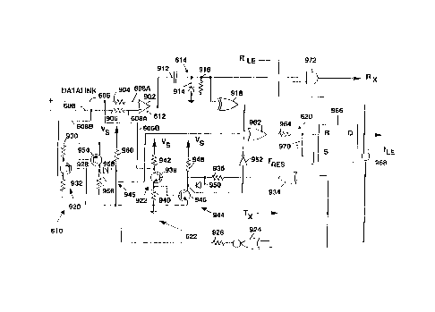
With reference to Fig. 9, an electrical
schematic of the first receiver 612, the first
transmitter 610, the first pinned fault detection
means 614, the first overcurrent detection means 618,
and the first fault status circuit 620 is shown. The
schematic fox the second receiver 613, the second
transmitter 611, the second pinned fault detection
means 615, and the second fault status circuit 621 is
identical and is therefore not further described. The
first receiver 612 includes a differential receiver
902. The first positive and negative transmission
wires 606,608 are connected to the negative and
positive input terminals of the differential receiver
902 through a first resistor 904 and a first positive
receiving wire 606A connected in series, and through a
second resistor 906 and a first negative receiving
wire 608A, respectively. The output of the
differential receiver 902 is the complement of the
logic state on the transmission line 510, i. e. , 'o~iToo
or "LO".
WO 91/17515 PCT/U~90/04677
~14~
The pinned fault detection means 614
includes a first capacitor 9l2 connected to the output
of the differential receiver 902 at one end and to the
fourth logic gate 722 at the other end. The juncture
between the first capacitor 912 and the fourth logic
gate 722 is connected to ground by a first diode 914
and a fifth resistor 916 connected in parallel. The
juncture is also connected to an input of a fifth
logic gate 918. A second input of the fifth logic
gate 918 is connected to the output of the
differential receiver 902.
The transmitter 610, in the preferred
embodiment, has a negative line driver 920 and a
positive line driver 922. The negative line driver
920 includes a sixth logic gate 924. The sixth logic
gate 924 receives signal TX. A sixth resistor 926 is
connected to the output of the sixth logic gate 924 at
one end and to the base of a first PNP transistoa~ 928
at the other end. The emitter of the first PNP
transistor 928 is connected to the voltage supply, VS,
through a seventh resistor 930. The collector of the
first PNP transistor 928 is connected to electrical
ground through an eighth resibtor 932 and is also
connected to the feirst negative transmission wire 608
through a first negative transmitting wire 608B.
The positive line driver 922 includes a
seventh logic gate 934. An input of the seventh logic
gate 934 receives signal TX. A ninth resistor 936 is
connected to the output of the seventh logic gate 934
at one end and to the base of a first NPN transistor
938 at the other end. The emitter of the first NPN
transistor 938 is connected to electrical ground by a
tenth resister 940. An eleventh resistor 942 connects
the collector of the first NPN transistor 938 to the
voltage supply. VS~ The collector of the first NPN
W~ 91/17615 PCT/US90/04677
a ~ s~
YJ
transistor 938 is also connected to the first positive
transmission wire 606 through a first positive
transmitting wire 606B.
The first overcurrent detection.means 618
includes a positive overcurrent detection circuit 944
and a negative overcurrent detection circuit 945. The
positive overcurrent detection circuit 944 includes a
second NPN transistor 946, the base of which is
connected to the emitter of the first NPN transistor
ZO 938 and the emitter of the second NPN transistor 946
is connected to electrical ground. A twelfth resistor
948 connects the collector of the second NPN
transistor 946 to the voltage supply, V8. A second
diode 950 is connected between the base of the first
NPN transistor 938 and the collector of the second NPN
transistor 946. The collector of the second NPN
transistor 946 is also connected to an eighth logic
gate 952. The negative overcurrent detection circuit
945 Includes a second PNP transistor 954, the base of
which is connected to the emitter of the first PNP
transistor 928 and the emitter of the second PNP
translator 954 is connected to the voltage supply, Vs.
A thirteenth resistor 956 connects the collector of
the second PNP transistor 954 to electrical ground. A
third diode 958 connects the collector of the second
PNP transistor 954 to the ;::ase of the first PNP
transistor 928. A fourteenth resistor 960 connects
the cathode of the third diode 958 to the voltage
supply, VS~
The first fault status circuit 620 includes
a logic gate 962. An input of the logic gate 962 is
connected to the output of the fifth logic gate 918.
A second input of the logic gate 962 is connected to
the collector of the second PNP transistor 954 and a
third input of the logic gate 962 is connected t~ the
WO 91/17615 PCT/US9a/Oa677
-16-
~~ ~ y _'~. 6~
collector of the second NFN transistor 946 through the
eighth logic gate 952. A fifteenth resistor 964 is
connected between the output of the logic gate 962 and
the Reset terminal of a flip-flop 966. A second
capacitor 970 connects the Reset terminal of the
flip-flop 966 to electrical ground. The flip-flop 966
is under the control of the microprocessor 602 through
the Set terminal (signal FMS). The output terminal,
Q, of the flip-flop 966 is connected to the
microprocessor 602 and to the sixth and seventh logic
gates 924,934 through a logic gate 968. The tenth
logic gate is also responsive to the signal T~. An
eleventh logic gate 972 is connected to the pinned
fault detection.means 614, the flip-flap 966, and
signal Rte.
Industrial Applieabl~stv
With reference to the drawings, and in
operation the networ& 500 is adapted for communication
betweew three control modules 502A,5028,502C on an
earthmoving vehicle, for example, an excavator or a
wheel loader, not shown. The contxol modules
502A,502B,503C have varying functions. These control
modules 502A,502B,50C periodically generate data
messages which may be needed by one or more of the
other control modules 502A,502B,502C. If no data
message is being transmitted by any control module
502, all transmission lines 510 are in the passive or
logic level ''HI" state.
For example in a typical embodiment, one
control module 502A controls the fuel injection of the
vehicle's engine: The second control module 502B
controls the actuation of the clutches and brakes in
an electrohydraulic transmission. The third control
W~ 91/17615 F°C,°T/1J590/04677
;t, n
17 _ ~-~) ~ 9 .~. ~ c~
i.d
module 5020 controls the movement/position of the
implement, i.e., bucket.
The control modules 502A,502B,502C need to
communicate to perform their assigned tasks. The
first control module 502A includes a sensor for
monitoring the engine's RPM. The second control
module 5028 may also require the engine's RPM to
determine a desired gear ratio. Therefore, the first
control module 502A needs to periodically transmit the
engine's RPM to the second control module 502B.
To accomplish this, the first control module
502A checks if either of the other control modules
5028,5020 is transmitting a data message. This is
accomplished through the detecting means 708. The
first logic gate 710 compares the signals, RX and T~.
Since no message is being transmitted by the first
control module 502A, signal T~ is "HI", the pas:cive
state. Therefore the output of the first logic gate
?10 Will be "HI" only if signal R~ is '°L0" (i.e., the
2o second or third control module 5028,502 is
transmitting a data message). The lowpass filter 714
eliminates any high frequency transients in the output
of the first logic gate 710. When the output of the
first logic gate 710 goes "HI", the flip~flop 712 will
be "set", i.e., the flip--flop's output, Q, and signal
SBD go °'HI". After signal S$D goes "HI", the
microprocessor 602 of the first control module 502A
delays transmission of the data message containing the
engine°s RPM for a period of time greater than the ,
time required to transmit one character of data
(discussed above). At that time, the first control
module 502A will~try to transmit the data message
again, until it is successful, i.e., the other control
module 5028,5030 is done transmitting.
W~ 91/17615 P~.'f/US90/04677
~~~ fi ~ ~°~ -ls-
While the first control module 502A is
transmitting its data message, the second control
module 5028 receives the data message from the first
transceiver 504B and passes the data message to the
third control module 502C by the passwthrough means
802, as described above. The data message is also
transmitted in the other direction by the first
transceiver 504A of the first control module 502A. w
The second transceiver 5060 of the third control
l0 module 502C receives the data message and passes the
data message to the second control module 502B. The
second and third control modules 502B,502C also decode
the data and detex~ine if the data is intended for
them through the Message Identification character
(MID) .
The chance occurrence that two control
modules 502A,502B,502C will transmit data messages
simultaneously is also eliminated by the detecting
means 708. The first logic gate 710 compares the
transmitted signal and the received signal, Tx and RX.
The detecting means a08 signals the microprocessor 602
when the signals are not the same. For examp3e, if
the first and second control.modul~s 502A,502B begin
to transaait.data messages at the same time, both will
continue to transmit as long as TX and I~ are the
same. However, if the first control module 502A
attempts to transmit a "HI" while the second control
module 5028 is transmitting a ''hO°', the microprocessor
602 of the first control module 502A will halt
transmission of its data message and wait in the same
mannex as described above. Signal SBD is also fed
into the second and third logic gates 720,721 to
disable the first and second transmitters 610,t1i of
the first control module 502A. Since the '°I3I"
transmitted by the first control module 502A is the
WO 91/17615 PCT/US90/04677
J Y ~ ' 1 YY
v .~ ~. S:' ~.J
passive state of the transmission lines, the
transmission lines will assume the '°LCa" being
transmitted by the second control modules 5028.
Therefore, the second control module 5028 can continue
to transmit its data message because the integrity of
its transmission has not been interrupted.
If the first differential receiver 902 is
receiving valid data, the output of th.e differential
receiver 902 is the logic complement of the state of
the transmission line 510 (an additional logic gate
can invert this signal before it reaches the
microprocessor 602 or the microprocessor 602 can
invert the dataj. Since the~voltage potential across
the capacitor 912 cannot change instantaneously, the
voltage across the fifth resistor 916 follows the
output of the differential receiver 620. If the
positive and negative transmission wires 606,608 are
shorted in the DOMINANT state, the output of the
differential receiver 612 remains "HI" for a period of
time great enough to charge the first capacitor 912.
The voltage potential across the fifth resistor 916
will fall as the voltage potential across the first
capacitor 912 rises. Therefore the inputs of the
fifth logic gate 918 will be apposite and the output
of the fifth logic gate 918 will go °'HI", triggerineJ
the first fault status circuit 620.
The first overcurrent detection means 618
includes the positive overcurrent detection circuit
944 and the negative overcurrent detection circuit
945, as described above. If the positive transmission
wire 606 is shorted to the supply voltage VS, the
magnitude of the current flowing through the tenth
resistor 940 increases. The voltage potential across
the tenth resistor 940 is linearly proportional to the
magnitude of the current flowing through the tenth
Vt'O 91/17615 PCT/U594l04677
resistor 940. When the voltage potential across the
tenth resistor 940 reaches a predetermined value, the
second NPN transistor 946 switches to the conducting
state and the voltage potential across the twelfth
5 resistor 948 increases. The input of the eighth logic
gate 952 becomes low, triggering the first fault
status circuit 620. If the negative t~:ansmission wire
608 is shorted to electrical ground, the magnitude of
the current flowing through the seveni:h resistor 930
10 increases. The voltage potential across the seventh
resistor 93o is, linearly proportional to the magnitude
of the current flowing through the seventh resister
930. When the voltage potential across the seventh
resistor 930 reaches a predetermined value, the second
l5 PNP transistor 954 switches to the conducting state
and the voltage potential across the thirteenth
resistor 956 increases, triggering the first fault
status circuit 620. Tf the first positive and
negative transmission wires 606,608 are shorted
20 together one or both of the positive and negative
overcurrent detection circuits 944;945 will trigger .
the first fault status circuit 620.
Tri this manner, the first fault status
circuit 620 relays to the microprocessor 602 the
presence of a short circuit on the first positive and
negative transmission wires 606,60. The
microprocessor 602 protects the circuit by disabling
the first receiver 612 and the first positive and
negative line drivers 920,922 signals T~,R~). The
second receiver 613 and the second positive and
negative line drivers 921,923 in the control module
502A,502B,502C on the other side shorted transmission
wires 606,608 are disabled in the same manner. Data
messages are transmitted around the network 500 in the
'WO 91/17615 ~C.°T/US90/04677
~'?G~~ ~I '~ ;a
_ 21.. 'S,i (: . ~. ~ n
other direction, bypassing 'the disabled
receivers/transmitters 612,613,920,921,922,923.
Transmission between all of the control
modules 502A,502B,502C can also be accomplished when a
break occurs in the transmission line
510AB,510BC,510CA between two of the control modules
502A,502B,502C. The receiversftransmitters
612,613,920,921,922,923 associated With the faulted
transmission line 510A8,510BC,510GA are disabled and
data messages are transmitted around 'the network in
the other direction, bypassing the disabled
receivers/transmitters 612,613,920,921,922,923. The
presence and location of the broken transmission line
510AB,510BC,510CA is determined in the following
manner. The first control module 502A (the assignment
of this function is arbitrary) periodically disables
the first transmitter 610 and transmits a data message
around 'the network in one direction using the second
transmitter 611. Tf the data mess~ege returns to the
first control module 502A and is received by the first
receiver 612, then no break has occurred. if the data
message does not return, a break in one of the
tranSml.SSlOn lines 51I~AB,51~BC,51~CA has oCCUrred.
Then the,first control module 502A requests that every.
other control module 5028,5020 transmit a data message
in turn. By monitor~.ng if the data message
transmitted by each control module 502B,502C is
received by the first or second transceiver 504,506,
the location of the break can be determined. for
example, if a break occurs between the first and
second Control modules 502A,5028, the data message
transmitted by the second control module 502B ArlD the
data message transmitted by the third control module
5020 will both be received by the second transceiver
504A of the the first control module.
A display (not shown) on the vehicle may
indicate to an operator that a fault has occurred and
the location of the fault. The outputs of the first
and second pinned fault detection means 614,615, and
the first positive and negative overcurrent detection
circuits may be connected to the microprocessor 602,
such that the microprocessor 602 can determine not
only the presence and location of a fault, but also
the type of fault present on the transmission lines
510AB,510BC,510CA.
20
35
..... - ;. :, , . ,.:,. . , ,.:,.. ; .,.,, ;,,, . , ,; . :.,,,,
: . ,,. ". . , .. . ' ,, .,,.. ~ , ( , , ,.,.. , .v : ;; , ' ",
.; ,; ... ~ .: ,' . . -... ,' .. ..: :: .< :' ..
, . ..; .
.; "
. :, .. ;, y
~ .~ .
; . ..:
,, . ~.
. ;~ , -..;
:,
.
'
.
~ ~
'
"
~
, ...
. .
. .,.
. .. y,,
, , .
:,. .
,
..
.. ,
.. ,
.
.,; .
.
..:
,, ,:. : . ~.:'. ~.'~ ~. ..~ .:.
;.; '.,, ,. , . ,.. ,~:'' ~..,-. , ,~ ' ':,'.,, ',..,... ) ,..,.
.,._:.:, .~:.v.' . :' ~" ,.~,',,... . ~ .. ., .' . . ;
. ' ~,~: ', ' ,~~ ' '~' . .,.,: . . :,. "':, , ' . . ,
. :.. '..,