Note: Descriptions are shown in the official language in which they were submitted.
- 1 - 20814~1
DIELECTRIC RESONATOR DEVICE AND
MANUFACTURING METHOD THEREOF
BACKGROUND OF THE INVENTION
l. Field of the Invention
The present invention generally relates to a
dielectric resonator arrangement, and more particularly,
to a dielectric resonator device constructed by forminy
a plurality of resonator electrodes on a dielectric
substrate or dielectric block.
2. Description of the Prior Art
Conventionally, there have been employed a multi-
stage dielectric resonator device constituted by forming
a plurality of resonance electrodes (inner electrodes)
within a dielectric block, and a ground electrode over
the outer face of said dielectric block, and a strip-
~ line type multi-stage resonator device having a
plurality of resonance electrodes formed on the surface
of a dielectric substrate, and a ground electrode formed
on a confronting surface of said dielectric substrate,
for example, as a band-pass filter, etc. in a microwave
band region.
In the dielectric resonator device having a
plurality of inner electrodes formed within the
dielectric block, coupling bores or holes are formed to
achieve coupling among respective resonators for setting
of the amount of coupling by the size of such coupling
bores. However, in this type of the resonator device in
which the coupling bores are to be provided, not only
the productivity is low in the manufacture, but it has
been difficult to adjust the coupling amount properly.
SUMMARY OF THE INVENTION
Accordingly, an essential object of the present
invention is to provide a dielectric resonator device
constituted by providing resonance electrodes on a
dielectric member, which is arranged to obtain necessary
'~'
_ - 2 - 2081144
characteristics without changing intervals between the
neighboring resonance electrodes.
Another object of the present invention is to
provide the dielectric resonator device of the above
described type in many kinds which are different in
characteristics without increasing kinds of molding
metal modes for manufacturing thereof.
A further object of the present invention is to
provide a method of manufacturing the dielectric
resonator device of the above described type in an
efficient manner at low cost.
In accomplishing these and other objects, according
to the present invention, there are provided the
dielectric resonator device and the method of
manufacturing said dielectric resonator device
characterized in the points as follows.
The dielectric resonator device of the present
invention is characterized in that it includes a
dielectric block having a first face and a second face
generally parallel to each other, side faces continuous
between said first and second faces, and through-holes
extending from the first face to the second face through
the dielectric block, an outer electrode formed over
said first face, said second face, and said side faces
of said dielectric block, and first inner electrodes and
second inner electrodes formed, through gaps, at least
in the vicinity of opening portions at one side, on
inner peripheral faces of said through-holes.
The dielectric resonator device according to the
present invention is further characterized in that it
includes a dielectric block having a first face and a
second face generally parallel to each other, side faces
continuous between said first and second faces and
through-holes extending from the first face to the
second face through the dielectric block, an outer
electrode formed over said first face, said second face,
_ ~ 3 ~ 2081~44
and said side faces of said dielectric block, and first
inner electrodes and second inner electrodes formed,
through gaps, in the vicinity of opening portions of
said first face, on inner peripheral faces of said
through-holes.
The method of manufacturing the dielectric
resonator device according to the present invention is
characterized in that it includes the steps of forming a
dielectric block having a first face and a second face
generally parallel to each other, side faces continuous
between said first and second faces, and through-holes
extending from the first face to the second face through
the dielectric block, applying, through formation, an
outer conductor film onto said first face, second face
and side faces of said dielectric block, and also,
applying, through formation, first inner conductor films
and second inner conductor films through gaps, at least
in the vicinity of opening portions at one side, onto
inner peripheral faces of said through-holes.
The method of manufacturing the dielectric
resonator device according to the present invention is
further characterized in that it includes the steps of
forming a dielectric block having a first face and a
second face generally parallel to each other, side faces
continuous between said first and second faces, and
through-holes extending from the first face to the
second face through the dielectric block, applying,
through formation, an outer conductor film onto said
first face, second face and side faces of said
dielectric block, and also, applying, through formation,
~irst inner conductor ~ilms and second inner conductor
films through gaps, in the vicinity of opening portions
of said first face, onto inner peripheral faces of said
through-holes.
The method of manufacturing the dielectric
resonator device according to the present invention is
~_ ~ 4 ~ 2081~44
further characterized in that the dielectric block is
formed through employment of common molding metal molds,
thereby to produce dielectric resonator devices having
various resonator characteristics by differentiating
5 widths of the gaps within the respective through-holes.
The method of manufacturing the dielectric
resonator device of the present invention is furthermore
characterized in that the dielectric bloc]~ is formed
through employment of common molding metal molds,
thereby to produce dielectric resonator devices having
various resonator characteristics by differentiating
positions and widths of the gaps within the respective
through-holes.
The dielectric resonator device of the present
invention is further characterized in that it includes a
dielectric block having a first face and a second face
generally parallel to each other, side faces continuous
between said first and second faces and through-holes
extending from the first face to the second face through
the dielectric block, an outer electrode formed over
said first face, said second face, and said side faces
of said dielectric block, and first inner electrodes and
second inner electrodes respectively formed, through
gaps, at least in the vicinity of opening portions at
one side on inner peripheral faces of said respective
through-holes.
The dielectric resonator device of the present
invention is still further characterized in that it
includes a dielectric block having a first face and a
second face generally parallel to each other, side faces
continuous between said first and second faces and
through-holes extending from the first face to the
second face through the dielectric block, an outer
electrode formed over said first face, said second face,
and said side faces of said dielectric block, and first
inner electrodes and second inner electrodes
~ ~.
- 5 - 2081444
respectively formed, through gaps, in the vicinity of
opening portion of said first face, on inner peripheral
- faces of said respective through-holes.
The method of manufacturing the dielectric
resonator device of the present invention is still
further characterized in that it includes the steps of
forming a dielectric block having a first face and a
second face generally parallel to each other, side faces
continuous between said first and second faces, and
through-holes extending from the first face to the
second face through the dielectric block, applying,
through formation, an outer conductor film onto said
first face, second face and side faces of said
dielectric block, and also, applying, through formation,
first inner conductor films and second inner conductor
films through gaps, at least in the vicinity of opening
portions at one side, onto inner peripheral faces of
- said respective through-holes.
The method of manufacturing the dielectric
resonator device of the present invention is furthermore
characterized in that it includes the steps of forming a
dielectric block having a first face and a second face
generally parallel to each other, side faces continuous
between said first and second faces, and through-holes
extending from the first face to the second face through
the dielectric block, applying, through formation, an
outer conductor film onto said first face, second face
and side faces of said dielectric block, and also,
applying, through formation, first inner conductor films
and second inner conductor films through gaps, in the
vicinity of opening portions of said first face, onto
inner peripheral faces of said respective through-holes.
The method of manufacturing the dielectric
resonator device of the present invention is further
characterized in that the dielectric block is formed
through employment of common molding metal molds,
,
- 2081444
thereby to produce dielectric resonator devices having
various resonator device characteristics by
differentiating positions of the gaps within the
respective through-holes.
The method of manufacturing the dielectric
resonator device of the present invention is furthermore
characterized in that the dielectric block is formed
through employment of common molding metal molds,
thereby to produce dielectric resonator devices having
various resonator device characteristics by
differentiating widths of the gaps within the respective
through-holes.
The method of manufacturing the dielectric
resonator device of the present invention is still
lS further characterized in that the dielectric block is
formed through employment of common molding metal molds,
thereby to produce dielectric resonator devices having
various resonator device characteristics by
differentiating positions and widths of the gaps within
the respective through-holes.
The dielectric resonator device of the present
invention is still characterized in that it includes a
dielectric substrate having resonance electrodes on its
first main surface and a ground electrode on its second
main surface, with the resonance electrodes being
conducted to said ground electrode in the vicinity of an
edge portion at one side of said dielectric substrate,
and auxiliary electrodes conducted to said ground
electrode and extending from the other edge portion of
said dielectric substrate which confronts said one edge
portion thereof, towards position near open ends of said
resonance electrodes.
The dielectric resonator device of the present
invention is further characterized in that it includes a
dielectric substrate having resonance electrodes on its
first main surface and a ground electrode on its second
`: ~
_ ~ 7 ~ 2081444
main surface, said resonance electrodes being adapted to
be open at opposite ends thereof, and auxiliary
electrodes conducted to said ground electrode and
extending from opposed two edge portions of said
dielectric substrate towards position near open ends of
said resonance electrodes.
The method of manufacturing the dielectric
resonator device of the present invention is still
characterized in that it includes the steps of forming a
dielectric substrate having resonance electrodes on its
first main surface and a ground electrode on its second
main surface, said resonance electrodes being conducted
to said ground electrode being adapted to be open at
opposite ends thereof, and also forming auxiliary
electrodes conducted to said ground electrode and
extending from opposed two edge portions of said
dielectric substrate towards position near open ends of
said resonance electrodes.
- The method of manufacturing the dielectric
resonator device of the present invention is furthermore
characterized in that it is arranged to produce
dielectric resonator devices having various resonator
characteristics by differentiating positions of gaps
between said resonance electrodes and said auxiliary
electrodes.
The method of manufacturing the dielectric
resonator device of the present invention is further
characterized in that it is arranged to produce
dielectric resonator devices having various resonator
characteristics by differentiating widths of gaps
between said resonance electrodes and said auxiliary
electrodes.
The method of manufacturing the dielectric
resonator device of the present invention is further
characterized in that it is arranged to produce
dielectric resonator devices having various resonator
2081~44
characteristics by differentiating positions and widths
of gaps between said resonance electrodes and said
auxiliary electrodes.
The dielectric resonator device of the present 5 invention is furthermore characterized in that it
includes a dielectric substrate having resonance
electrodes on its first main surface and a ground
electrode on its second main surface, said respective
resonance electrodes being conducted to said ground
electrode in the vicinity of an edge portion of said
dielectric substrate, and auxiliary electrodes conducted
to said ground electrode and extending from the other
edge portion of said dielectric substrate, towards
position near open ends of said respective resonance
electrodes respectively.
The dielectric resonator device according to the
present invention is still characterized in that it
includes a dielectric substrate having resonance
electrodes on its first main surface and a ground
electrode on its second main surface, said respective
resonance electrodes being adapted to be open at
opposite ends thereof, and auxiliary electrodes
conducted to said ground electrode and extending from
opposed two edge portions of said dielectric substrate
toward position near open ends of said respective
resonance electrodes respectively.
The method of manufacturing the dielectric
resonator device of the present invention is still
characterized in that it includes the steps of forming a
dielectric substrate having resonance electrodes on its
first main surface and a ground electrode on its second
main surface, said respective resonance electrodes being
conducted to said ground electrode in the vicinity of an
edge portion of said dielectric substrate, and also,
forming auxiliary electrodes conducted to said ground
electrode and extending from the other edge portion of
@;,
~ ~,, ~.
- 9 - 2081444
-
said dielectric substrate towards position near open
ends of said resonance electrodes respectively.
The method of manufacturing the dielectric
resonator device of the present invention is further
characterized in that it includes the steps of forming a
dielectric substrate having resonance electrodes on its
first main surface and a ground electrode on its second
main surface, said resonance electrodes being
respectively adapted to be open at opposite ends
thereof, and also forming auxiliary electrodes conducted
to said ground electrode and extending from opposed two
edge portions of said dielectric substrate, towards
position near open ends of said resonance electrodes
respectively.
The method of manufacturing the dielectric
resonator device of the present invention is still
further characterized in that it is arranged to produce
dielectric resonator devices having various resonator
device characteristics by differentiating respective
positions of gaps between said resonance electrodes and
said auxiliary electrodes.
The method of manufacturing the dielectric
resonator device of the present invention is furthermore
characterized in that it is arranged to produce
dielectric resonator devices having various resonator
device characteristics by differentiating respective
widths of gaps between said resonance electrodes and
said auxiliary electrodes.
The method of manufacturing the dielectric
resonator device of the present invention is
characterized in that it is arranged to produce
dielectric resonator devices having various resonator
device characteristics by differentiating respective
position and respective widths of gaps between said
resonance electrodes and said auxiliary electrodes.
FUNCTIONS
., ~
,~ ,ir~ '
-- - 208144 l
General functions of the dielectric resonator
device and the method of manufacturing said dielectric
resonator device according to the present invention as
referred to the above will be briefly explained herein
below.
- In the above dielectric resonator device of the
present invention, the dielectric block has the first
face and the second face generally parallel to each
other, the side faces continuous between said first and
second faces, and through-holes extending from the first
face to the second face through the dielectric block,
while the outer electrode is formed over said first
face, said second face, and said side faces of said
dielectric block, and the first inner electrodes and
second inner electrodes are formed, through gaps, at
least in the vicinity of opening portions at one side,
on the inner peripheral faces of said through-holes. As
stated above, at least one side of the first and second
inner electrodes formed in the inner peripheral face of
the through-holes within the dielectric block acts as
the resonance electrodes so as to functions as TEM mode
dielectric resonators.
In the above dielectric resonator device of the
present invention, the dielectric block has the first
face and the second face generally parallel to each
other, the side faces continuous between said first and
second faces, and through-holes extending from the first
face to the second face through the dielectric block,
with the outer electrode is formed over said first face,
said second face, and said side faces of said dielectric
block, and first inner electrodes and second inner
electrodes are formed, through gaps, in the vicinity of
opening portions of said first face, inner peripheral
faces of said through-hole. Of the first and second
inner electrodes formed on the inner peripheral faces of
the through-holes within the dielectric block, the inner
.^.,
~ ll- 2081~44
electrodes at one side contiguous to the outer electrode
on the second surface normally function as the TEM mode
dielectric resonators which resonate at 1/4 wavelength.
In the above method of manufacturing the dielectric
resonator device of the present invention, the
dielectric block having the first face and the second
face generally parallel to each other, the side faces
continuous between said first and second faces, and the
through-holes extending from the first face to the
second face through the dielectric block is formed, and
the outer conductor film is formed on said first face,
second face and side faces of said dielectric block, and
further the first inner conductor films and second inner
conductor films are formed through gaps, at least in the
vicinity of opening portions at one side, onto inner
peripheral faces of said through-holes. By the above
method, the outer conductor film formed on the first
face, the second face and the side faces act as the
outer electrode, while the inner conductor films at
least at one side of the first and second inner
conductor films formed in the inner peripheral surfaces
of the dielectric block function as the resonance
electrodes.
In the above method of manufacturing the dielectric
resonator device of the present invention, the
dielectric block having a first face and second face
generally parallel to each other, side faces continuous
between said first and second faces, and through-holes
extending from the first face to the second face through
the dielectric block is prepared, and the outer
conductor film is formed on said first face, second face
and side faces of said dielectric block, and also the
first inner conductor films and second inner conductor
films are formed through gaps, in the vicinity of
opening-portions of said first face, on the inner
peripheral faces of said through-holes respectively. By
B`
. .... ,.. ~s
- 12 ~ 2 0 81 4 14
the above method, the outer conductor film formed on the
first face, the second face and the side faces act as
the outer electrode, while the inner conductor films
contiguous from the opening portion of the second face
of the first and second inner conductor films formed on
the inner peripheral surfaces of the dielectric block
- function as the resonance electrodes, and thus, the
dielectric resonator device having the resonator length
of 1/4 wavelength is obtained.
In the above method of manufacturing the dielectric
resonator device of the present invention, tlle
dielectric block is formed through employment of common
molding metal molds, and the dielectric resonator
devices having various resonator characteristics are
obtained by differentiating positions of the gaps within
the respective through-holes. By the positions of the
above gaps, the lengths of the inner conductor films at
least at one side acting as the resonance electrodes are
varied, whereby in spite of the use of the dielectric
block formed by the common molding metal molds, the
dielectric resonator device having the predetermined
resonator characteristics may be obtained.
In the above method of manufacturing the dielectric
resonator device of the present invention, the
dielectric block is formed through employment of common
molding metal molds, and the dielectric resonator
devices having various resonator characteristics are
obtained by differentiating widths of the gaps within
the respective through-holes. By the size of the widths
for the gaps, the capacity produced between the first
and second inner electrodes is varied, whereby in spite
of the use of the dielectric block formed by the common
metal molds, the dielectric resonator device having the
predetermined resonance characteristics may be obtained.
In the above method of manufacturing the dielectric
resonator device of the present invention, the
B
--, , .
_ - 13 - 2081441
dielectric block is formed through employment of common
molding metal molds, and the dielectric resonator
devices having various resonator characteristics are
obtained by differentiating positions and widths of the
gaps within the respective through-holes. By the
positions of the above gaps, the lengths of the inner
conductor films at least at one side acting as the
resonator electrodes are varied, while, by the size of
widths for the gaps, the capacity produced between the
first and second inner electrodes is varied, whereby in
spite of the use of the dielectric block formed by the
common metal molds, the dielectric resonator device
having the predetermined resonance characteristics may
be obtained.
In the above dielectric resonator device of the
present invention, the dielectric block has the first
face and the second face generally parallel to each
other, side faces continuous between said first and
second faces, and the through-holes extending from the
first face to the second face through the dielectric
block, while the outer electrode is formed over said
first face, said second face, and said side faces of
said dielectric block, and first inner electrodes and
second inner electrodes are respectively formed, through
gaps, at least in the vicinity of opening portions at
one side, on inner peripheral faces of said respective
through-holes. As stated above, at least one side of
the first and second inner electrodes formed in the
inner peripheral face of the through-holes within the
dielectric block acts as the resonance electrodes so as
to function on the whole as TEM mode dielectric
resonator device of a plurality of stages.
In the above dielectric resonator device of the
present invention, the dielectric block has the first
face and the second face generally parallel to each
other, side faces continuous between said first and
' '~
~8
- 20814 11
second faces and through-holes extending from the first
face to the second face through the dielectric block,
while outer electrode is formed over said first face,
said second face, and said side faces of said dielectric
block, and the first inner electrodes and second inner
electrodes are respectively formed, through gaps, in the
vicinity of opening portions of said first face, on the
inner peripheral faces of said respective through-holes.
Of the first and second inner electrodes formed on the
inner peripheral faces of the through-holes within the
dielectric block, the inner electrodes at one side
contiguous to the outer electrode on the second surface
normally function as the TEM mode dielectric resonator
device of a comb-like type which resonate at l/4
wavelength respectively.
In the above method of manufacturing the dielectric
resonator device of the present invention, the
dielectric block having the first face and the second
face generally parallel to each other, the side faces
continuous between said first and second faces, and
through-holes extending from the first face to the
second face through the dielectric block is formed, and
- the outer conductor film is formed on said first face,
second face and side faces of said dielectric block, and
also, first inner conductor films and second inner
conductor films are formed through gaps, at least in the
vicinity of opening portions at one side, onto the inner
peripheral faces of said respective through-holes. By
the above method, the outer conductor film formed on the
first face, the second face and the side faces act as
the outer electrode, while the inner conductor films at
least at one side of the first and second inner
conductor films formed on the inner peripheral surfaces
- of the dielectric block function as the resonance
electrodes, and thus, the dielectric resonator device of
the plurality of stages may be obtained.
B `
~.. ~ ....
_ - 15 - 2081444
In the above method of manufacturing the dielectric
resonator device of the present invention, the
dielectric block having the first face and the second
face generally parallel to each other, side faces
S continuous between said first and second faces, and the
through-holes extending from the first face to the
second face through the dielectric block is formed, and
the outer conductor film is formed on said first face,
second face and side faces of said dielectric block, and
also, the first inner conductor films and second inner
conductor films are formed through gaps, in the vicinity
of opening portions of said first face, on the inner
peripheral faces of said respective through-holes. By
the above method, the outer conductor film formed on the
first face, the second face and the side faces act as
the outer electrode, while the inner conductor films
contiguous from the opening portion of the second face
of the first and second inner conductor films formed on
the inner peripheral surfaces of the dielectric block
function as the resonance electrodes, and thus, the
dielectric resonator device of a plurality of stages
having the resonator length of 1/4 wavelength is
obtained.
In the above method of manufacturing the dielectric
resonator device of the present invention, the
dielectric block is formed through employment of common
molding metal molds, and the dielectric resonator
devices having various resonator device characteristics
are obtained by differentiating positions of the gaps
within the respective through-holes. By the positions of
the above gaps, the lengths of the inner conductor films
at least at one side acting as the resonance electrodes
are varied, whereby in spite of the use of the
dielectric block formed by the common molding metal
molds, the dielectric resonator device having the
predetermined resonance characteristics may be obtained.
.. ~
~D
~j5 .... -
~_ - 16 ~ 2081444
In the above method of manufacturing the dielectric
resonator device of the present invention, the
dielectric block is formed through employment of common
molding metal molds, and the dielectric resonator
devices having various resonator characteristics are
obtained by differentiating widths of the gaps within
the respective through-holes. By the size of the widths
for the gaps, the capacity produced between the first
and second inner electrodes is varied, whereby in spite
of the use of the dielectric block formed by the common
metal molds, the dielectric resonator device having the
predetermined resonator device characteristics may be
obtained.
In the above method of manufacturing the dielectric
resonator device of the present invention, the
dielectric block is formed through employment of common
molding metal molds, and the dielectric resonator
devices having various resonator device characteristics
by differentiating positions and widths of the gaps
within the respective through-holes. By the positions
of the above gaps, the lengths of the inner conductor
films at least at one side acting as the resonance
electrodes are varied, while, by the size of the width
- for the gaps, the capacity produced between the first
and second inner electrodes is varied, whereby in spite
of the use of the dielectric block formed by the common
metal molds, the dielectric resonator device having the
predetermined resonance characteristics may be obtained.
In the above dielectric resonator device of the
present invention, the dielectric substrate has
resonance electrodes on its first main surface and a
ground electrode on its second main surface, with the
resonance electrodes being conducted to said ground
electrode in the vicinity of an edge portion at one side
of said dielectric substrate, and the auxiliary
electrodes are conducted to said ground electrode and
_ - 17 ~ 20814~4
extending from the other edge portion of said dielectric
substrate which confronts said one edge portion thereof,
towards position near open ends of said resonance
electrodes. By the above arrangement, the resonator
device may be used as a strip-line resonator.
In the above dielectric resonator device of the
present invention, the dielectric substrate has the
resonance electrodes on its first main surface and the
ground electrode on its second main surface, with the
resonance electrodes being adapted to be open at
opposite ends thereof, and the auxiliary electrodes are
conducted to said ground electrodes and extending from
opposed two edge portions of said dielectric substrate
towards position near open ends of said resonance
electrodes. By the above structure, the resonator
device can be used as a strip-line resonator.
In the above method of manufacturing the dielectric
resonator device of the present invention, the
dielectric substrate having the resonance electrodes on
its first main surface and a ground electrode on its
second main surface is formed, with the resonance
electrodes being conducted to said ground electrode in
the vicinity of an edge portion at one side of said
dielectric substrate, and also, auxiliary electrodes are
conducted to said ground electrode and extending from
the other edge portion of said dielectric substrate
which confronts said one edge portion thereof, towards
position near open ends of said resonance electrodes,
whereby the dielectric resonator device is produced.
In the above method of manufacturing the dielectric
resonator device of the present invention, the
dielectric substrate having the resonance electrodes on
its first main surface and the ground electrode on its
second main surface is formed, with the resonance
electrodes being adapted to be open at opposite ends
thereof, and also, auxiliary electrodes are conducted to
~ .~
, _~,~ . , .i,,
- 18 ~ 208144~
said ground electrode and extending from opposed two
edge portions of said dielectric substrate, towards
position near open ends of said resonance electrodes,
and thus, the dielectric resonator device is produced.
s In the above method of manufacturing the dielectric
resonator device of the present invention, it is
arranged to produce dielectric resonator devices having
various resonator characteristics by differentiating
positions of gaps between said resonance electrodes and
said auxiliary electrodes. By the positions of the
above gaps, the lengths of the resonance electrodes are
varied, whereby in spite of the use of the common
dielectric substrates, the dielectric resonator device
having the predetermined resonance characteristics may
be obtained.
In the above method of manufacturing the dielectric
resonator device of the present invention, it is
arranged to produce dielectric resonator devices having
various resonator characteristics by differentiating
widths of gaps between said resonance electrodes and
said auxiliary electrodes. By the widths for the gaps,
the capacity produced between the resonance electrode
and auxiliary electrodes is varied, whereby in spite of
the use of the common dielectric substrate, the
dielectric resonator device having the predetermined
resonance characteristics may be obtained.
In the above method of manufacturing the dielectric
resonator device of the present invention, it is
arranged to produce dielectric resonator devices having
various resonator characteristics by differentiating
positions and widths of gaps between said resonance
electrodes and said auxiliary electrodes. By the
positions of the above gaps, the lengths of the
resonance electrodes are varied, while, by the size of
the widths, the capacity produced between the resonance
and auxiliary electrodes is varied, whereby in spite of
B
- lg - 2081444
the use of common dielectric substrate, the dielectric
resonator device having the predetermined resonance
characteristics may be obtained.
In the dielectric resonator device of the present
S invention, the dielectric substrate has the resonance
electrodes on its first main surface and a ground
electrode on its second main surface, respective
resonance electrodes being conducted to said ground
electrode in the vicinity of an edge portion of said
dielectric substrate, and the auxiliary electrodes are
~ conducted to said ground electrode and extending from
the other edge portion of said dielectric substrate
towards position near open ends of said respective
resonance electrodes respectively. By the above
construction, the dielectric device may be used as a
strip-line filter.
In the dielectric device of the present invention,
the dielectric substrate has the resonance electrodes on
its first main surface and a ground electrode on its
second main surface, with the respective resonance on
its second main surface, with the respective resonance
electrodes being adapted to be open at opposite ends
thereof, and the auxiliary electrodes are conducted to
said ground electrodes and extending from opposed two
edge portions of said dielectric substrate towards
position near open ends of said respective resonance
electrodes respectively. The above construction makes
it possible to use the resonator device for a strip-line
filter.
In the method of manufacturing the dielectric
resonator device of the present invention, the
dielectric substrate having the resonance electrodes on
its first main surface and the ground electrode on its
second main surface is formed, with the respective
resonance electrodes being conducted to said ground
electrode in the vicinity of an edge portion of said
~ - 20 ~ 2081444
dielectric substrate, and also, the auxiliary electrodes
are conducted to said ground electrode and extending
from the other edge portion of said dielectric substrate
towards portion near open ends of said resonance
electrodes respectively.
In the method of manufacturing the dielectric
resonator device of the present invention, the
dielectric substrate having resonance electrodes on its
first main surface and a ground electrode on its second
main surface is formed, with the resonance electrodes
being respectively adapted to be open at opposite ends
thereof, and the auxiliary electrodes are conducted to
said ground electrode and extending from opposed two
edge portions of said dielectric substrate towards
position near open ends of said resonance electrodes
respectively.
In the method of manufacturing the dielectric
resonator device of the present invention, it is
arranged to produce dielectric resonator devices having
various resonator device characteristics by
differentiating respective positions of gaps between
said resonance electrodes and said auxiliary electrodes.
By the positions of the above gaps, the lengths of the
resonance electrodes are varied, whereby in spite of the
use of the common dielectric substrate, the dielectric
resonator device having the predetermined resonance
characteristics may be obtained.
In the method of manufacturing the dielectric
resonator device of the present invention, it is
arranged to produce dielectric resonator devices having
various resonator device characteristics by
differentiating respective widths of gaps between said
resonance electrodes and said auxiliary electrodes. By
the widths for the gaps, the capacity produced between
the resonance electrode and auxiliary electrodes is
varied, whereby in spite of the use of the common
;5~ B
_ - 21 - 2081444
dielectric substrate the dielectric resonator device
having the predetermined resonance characteristics may
be obtained.
In the method of manufacturlng the dielectric
s resonator device of the present invention, it is
arranged to produce dielectric resonator devices haviny
various resonator device characteristics by
differentiating respective positions and respective
widths of gaps between said resonance electrodes and
said auxiliary electrodes. By the positions of the
above gaps, the lengths of the resonance electrodes are
varied, while by the size of the widths, the capacity
produced between the resonance and auxiliary electrodes
is varied, whereby in spite of the use of the common
dielectric substrate, the dielectric resonator device
having the predetermined resonance characteristics may
be obtained.
BRIEF DESCRIPTION OF THE DRAWINGS
These and other objects and features of the present
invention will become apparent from the followiny
description taken in con~unction with the preferred
embodiment thereof with reference to the accompanying
drawings, in which:
FIG. l(A) is a front elevational view of a
dielectric resonator device according to one preferred
embodiment of the present invention,
FIG. l(B) is a cross section taken along the line
I(B)-I(B) in Fig. l(A),
FIG. 2 is a perspective view of the dielectric
resonator device of Fig. l(A),
FIG. 3 (A) iS a top plan view of a dielectric
resonator device according to a second embodiment of the
present invention,
FIG. 3(B) is a cross section taken along the line
III(B)-III(B) in Fig. 3(A),
'. ~
_ - 22 - 2081444
FIG. 4(A) is a front elevational view of a
conventional dielectric resonator device (already
referred to),
FIG. 4(B) is a cross section taken along the line
IV(B)-IV(B) in Fig. 4(A) (already referred to),
FIG. 5 is an equivalent circuit diagram of a
symmetrical 4 stage band-pass filter, and
FIG. 6 is an equivalent circuit diagram of a 2
stage comb-like type filter.
DESCRIPTION OF THE PRIOR ART
Figures 4(A) and 4(B) represent the prior art
dielectric resonators and wherein Fig. 4(A) is a top
plan view of a conventional dielectric resonator device,
and Fig. 4(B) is a side sectional view taken along the
line IV(B)-IV(B) in Fig. 4(A).
In Figs. 4(A) and 4(B), the known resonator device,
for example, in the form of a symmetrical 4 stage band-
pass filter, includes a dielectric block l' formed
therein with four through-holes, and inner electrodes
2a', 2b', 2c' and 2d' formed in the inner peripheral
faces of said through-holes. The dielectric resonator
device as referred to above may be represented by an
equivalent circuit as shown in Fig. 5, in which Rl, R2,
R3 and R4 denote the resonators formed by the inner
electrodes 2a', 2b', 2c' and 2d' as shown in Figs. 4(A)
and 4(B), with symbols Kl and K2 representing the
coupling amounts between the respective neighboring
resonators. In the dielectric resonator device having
the constructions as illustrated in Figs. 4(A) and 4(B),
for example, the resonance frequency of the resonator R2
is determined by a length L2' of the inner electrode Zb'
of the inner electrode 2b' at a second stage, while the
coupling amount K2 is determined by a length S2' of a
region not formed with the inner electrode, and an
interval P2' between the inner electrodes 2b'-2c'.
~3 `
.~ ... ., ~
- 23 ~ 2081444
When a filter is to be designed in a relation
represented by fl>f2 and Kl>K2 on the assumption that
the dielectric resonator device shown in Figs. 4(A) and
4(B) is constructed as the symmetrical 4 stage band-pass
filter, and the resonance frequencies of the resonators
Rl and R4 are represented by fl, and those of the
resonators R2 and R3, by f2, the procedure for the
design will be as follows.
(i) To determine the length L2' of the inner
electrodes 2b' and 2c' according to the resonance
frequencies f2.
(ii) To determine the length S2' of the inner
~ electrode non-formed region and/or the interval P2'
between the inner electrodes 2b'-2c' according to the
coupling amount K2, with consequent determination of the
axial length L thereby.
(iii) To determine the length Ll' of the inner
electrodes 2a' and 2b' according to the resonance
frequency fl, with consequent determination of Sl'.
(iv) To determine the interval Pl' between the
inner electrodes 2a'-2b' and 2c'-2d' according to the
coupling amount Kl.
Although the symmetrical 4 stage band-pass filter
may be designed in the manner as described above, since
the interval Pl' and P2' between the inner electrodes
are not constant according to the filter characteristics
aimed at, different metal molds are required for each
kind of the filters, thus resulting in high
manufacturing cost.
DETAILED DESCRIPTION OF THE INVENTION
Before the description of the present invention
proceeds, it is to be noted that like parts are
designated by like reference numerals throughout the
accompanying drawings.
Referring now to the drawings, there is shown in
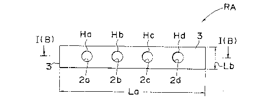
Figs. l(A), l(B) and 2, a dielectric resonator device RA
'
~ - 24 ~ 20814~1
according to one preferred embodiment of the present
invention, which generally includes a dielectric bloc]~ 1
in the form of a hexahedron or in a rectangular cubic
box-like configuration having a first face A and a
second face B which are generally parallel to eacll other
and side faces C, D, E and F contiguously provided
between said first and second faces, four though-lloles
Ha, Hb, Hc and Hd formed to extend through the
dielectric block 1 from the first face A to the second
face B, first inner electrodes 2a, 2b, 2c and 2d and
, ......
` -
208114~
-
second inner electrodes 8a, 8b, 8c and 8d respectively formed
- in the inner peripheral faces of the respective through-holes
Ha to Hd, and an outer electrode 3 formed on the first face
A, the second face B, and the side faces C, D, E and F.
The dielectric block l is formed through employment
of a molding metal mold which serves as a standard (not
particularly shown). Although the dielectric block to be
obtained by one metal mold has the same shape and same
dimensions on the whole, including positions of the through-
holes Ha to Hd, resonator devices having different resonator
characteristics may be obtained by the lengths of the first
inner electrodes 2a to 2d and the second inner electrodes 8a
to 8d to be formed on the respective inner peripheral faces
of said through-holes Ha to Hd. By way of example, it becomes
possible to constitute a plurality of kinds of band-pass
filters different in center frequencies and band widths, etc.
by the use of the dielectric block produced by the common
molding metal mold.
Subsequently, referring to Fig. 6, showing an
e~uivalent circuit diagram of a general 2 stage comb-line type
filter, factors determining the center frequencies and band
widths will be explained.
In the first place, the center frequency fo is
represented by an equation as follows from the resonance
condition.
,~ G
- 2081441
2~foCs = Ya.cot ~o
- ~o = ~(r)/C~-2~foL
where ~r is a dielectric constant of a resonator surrounding
substance, Cs is a straight capacity, L is a resonator length,
Ya is admittance of the resonator, and C is a light velocity.
Meanwhile, a coupling coefficient k is represented by a
following equation, and is determined by each admittance and
.
k = {(Yo-Ye)/Ya~ l(l + ~o/(sin ~o-cos ~o)~1
where Yo is an admittance in the odd mode, and Ye is an
admittance in the even mode.
Subsequently, specific examples will be shown by
referring to Figs. l(A) and l(B).
In Figs. l(A) and l(B), there is shown a dielectric
resonator device RA according to one preferred embodiment of
the present invention, which comprises a dielectric block 1
having a first face and a second face B generally parallel to
each other, side faces continuous between the first and second
faces A and B, and through-holes Ha, Hb, Hc and Hd extending
from the first face A to the second face B through the
dielectric block 1, an outer electrode 3 formed over the first
face A, the second face B, and the side faces of said
dielectric block 1, and first inner electrodes 2a, 2b, 2c and
2d and second inner electrodes 8a, 8b, 8c, and 8d formed,
through gaps 7a, 7b, 7c and 7d at least in the vicinity of
, ~,
,
2081444
opening portions at one side, on inner peripheral faces of
- said through-holes Ha to Hd.
More specifically, the first inner electrodes 2a,
2b, 2c, and 2d, and the second inner electrodes 8a, 8b, 8c,
and 8d are each formed on the inner peripheral faces of the
respective through-holes Ha, Hb, Hc and Hd through the gaps,
i.e. non-electrode forming regions 7a, 7b, 7c and 7d provided
therebetween, and one end of each of the inner electrodes 2a
to 2d and 8a to 8d is conducted to the outer electrode 3.
The first inner electrodes 2a to 2d act as resonance
electrodes, with the first face A of the dielectric block 1
functioning as a short-circuiting face. Lengths of the first
inner electrodes 2a, 2b, 2c and 2d are represented by Ll, L2,
L3 and L4, and widths of the gaps 7a, 7b, 7c and 7d are
denoted by S1, S2, S3 and S4 respectively. Meanwhile, the
lengths of the respective sides of the dielectric block are
represented by La, Lb and Lc, and the intervals between the
respective inner electrodes are represented by P1 between 2a
and 2b, P2 between 2b and 2c, and P3 between 2c and 2d. Here.
the relation for the respective internals may be set as
P1=P2=P3 or Pl~P2~P3~P1.
Although the resonance frequency of each resonator
is determined by various factors, in the embodiment as shown
in Figs. l(A) and l(B), the resonance frequency of the first
resonator by the first inner electrode 2a is determined by L1
B
.
2081444
and Sl, the resonance frequency of the second resonator by the
first inner electrode 2b is determined by L2 and S2, the
resonance frequency of the third resonator by the first inner
electrode 2c is determined by L3 and S3, and further, the
resonance frequency of the fourth resonator by the first inner
electrode 2d is determined by L4 and S4. Meanwhile, the
coupling amounts between the neighboring resonators are
determined by P1, P2 and P3, and Sl, S2, S3 and S4, and in
this case, the intervals Pl, P2 and P3 between the inner
electrodes to be set by the metal mold dimensions are fixed.
The dielectric resonator device RA as shown in Figs.
l(A) and l(B) functions as a band-pass filter "F1" having a
center frequency of fl, and a band width of BW1, but in order
to produce on a large scale, band-pass filters with different
characteristics by the dimensions of the first and second
inner electrodes within the respective through-holes through
employment of dielectric blocks prepared by the same metal
mold, such band-pass filters may be manufactured after
designing in the manner as described hereinbelow.
Firstly, in the case where a band-pass filter "F2"
with the band width equal to BWl, and the center frequency of
f2 higher than fl tf2>fl) is to be produced on a large scale,
the length of the first inner elec~trode 2a is set to be L12
shorter than L1, that of the first inner electrode 2b is set
2~ to be L22 shorter than L2, that of the first inner electrode
. .~ .
~ 2081~44
2c is set to be L32 shorter than L3, and that of the first
inner electrode 2d is set to be L42 shorter than L4. The
widths Sl, S2, S3 and S4 of the gaps 7a to 7d between the
first inner electrodes 2a to 2d, and the second inner
electrodes 8a to 8d, are set to be the same as in the case
where the center frequency is fl in principle, and according-
ly, the lengths of the second inner electrodes 8a to 8d are
set to be longer than those in the case of the band-pass
filter "F1". As described above, when the center frequency
is higher, each length of the second inner electrodes 8a to
8d becomes generally longer. However, in the case where the
center frequency f2 of this filter "F2" is spaced away from
he center frequency fl of the filter "F1" too far to neglect
the variation in the pass-band width, the widths S1, S2, S3
and S4 of the gaps are slightly increased, with corresponding
slight increase of the lengths L12, L22, L32, and L42 of the
first inner electrodes in design for manufacturing.
Then, for mass-production of the filter having the
pass-band width narrower than BWl, with the center frequency
set at f2, the widths Sl, S2, S3 and S4 are each increased at
the designing stage.
In the above case, if the influence over the
resonance frequency of each resonator can not be neglected due
to the alternation of the values for Sl, S2, S3 and S4, the
values for the lengths L12, L22, L32 and L42 of the respective
.~
, . . .
2081444
3~
first inner electrodes are altered in the directions towards
- L12 - Ll, L22 - L2, L32 ~ L3, and L42 - L4 respectively, and
simultaneously, the lengths of the second inner electrodes 8a,
8b, 8c and 8d are reduced by the amounts in which the lengths
of the first inner electrodes L12, L22, L32 and L42 are
increased respectively in the designing.
Conversely, for mass-production of the filter having
the pass-band width wider than BW1, with the center frequency
set at f 2, the widths Sl, S2, S3 and S4 are each reduced at
the designing stage.
In the above case, if the influence over the
resonance frequency of each resonator can not be neglected due
to the alternation of the values for S1, S2, S3 and S4, the
values for the lengths L12, L22, L32 and L42 of the respective
first inner electrodes are further reduced and simultaneously,
the lengths of the second inner electrodes 8a, 8b, 8c and 8d
are increased.
As described above, various kinds of filters as
desired are manufactured on a large scale by determining the
lengths of the first and second inner electrodes and the
widths of the gaps at the stage of designing. It is to be
noted here that the lengths of the respective electrodes and
the widths of the gaps as referred to above may be set at the
predetermined values by grinding the inner electrodes at the
gap portions through employment of a grained stone.
B
2081444
In the case where a band-pass filter "F3" with the
- band width equal to BWl, and the center frequency of f3 lower
than fl (f3<fl) is to be produced on a large scale, the length
of the first inner electrode 2a is set to be L13 longer than
Ll, that of the first inner electrode 2b is set to be L23
longer than L2, and that of the first inner electrode 2c is
set to be L33 longer than L3, and that of the first inner
electrode 2d is set to be L43 longer than L4. The widths S1,
S2, S3 and S4 of the gaps 7a to 7d between the first inner
electrodes 2a to 2d, and the second inner electrodes 8a to 8d,
are set to be the same as in the case where the center
frequency is fl in principle, and accordingly the lengths of
the second inner electrodes 8a to 8d are set to be shorter
than those in the case of the band-pass filter "Fl". As
described above, when the center frequency is lower, each
length of the second inner electrodes 8a to 8d becomes
generally shorter. However, in the case where the center
frequency f3 of this filter "F3" is spaced away from the
center frequency fl of the filter "Fl" too far to neglect the
variation in the pass-band width, the widths Sl, S2, S3 and
S4 of the gaps are slightly decreased, with corresponding
slight decrease of the lengths L13, L23, L33, and L43 of the
first inner electrodes in design for manufacturing.
Then, for mass-production of the filter having the
pass band width narrower than BWl, with the center frequency
~ `;
3~ 2081444
set at f3, the widths Sl, S2, S3 and S4 are each increased at
the designing stage.
In the above case, if the influence over the
resonance frequency of each resonator can not be neglected due
to the alternation of the values for S1, S2, S3 and S4, the
values for the lengths L13, L23, L33 and L43 of the respective
first inner electrodes are further increased, and
simultaneously, the lengths of the second inner electrodes 8a,
8b, 8c and 8d are reduced in the designing.
Conversely, for mass-production of the filter having
the pass and width wider than BWl, with the center frequency
st at f 3, the widths Sl, S2, S3 and S4 are each decreased at
the designing stage. In the above case, if the influence over
the resonance frequency of each resonator can not be neglected
due to the alternation of the values for Sl, S2, S3 and S4,
the values for the lengths L13, L23, L33 and L43 of the
respective first inner electrodes are altered in the direc-
tions towards L13 - Ll, L23 - L2, L33 - L3, and L43 - L4
respectively, and simultaneously, the lengths of the second
inner electrodes 8a, 8b, 8c and 8d are increased by the
amounts in which the lengths of the first inner electrodes
L12, L22, L32 and L42 are decreased respectively in the
designing.
As described above, various kinds of filter as
desired are manufactured on a large scale by determining the
B ~
. ~
2081444
33
lengths of the first and second inner electrodes and the
- widths of the gaps at the stage of designing.
In the manners as described so far, it may be so
arranged to obtain the dimensional data for each part which
will provide the desired characteristics at the stage of
designing or trial production, sand to carry out mass produc-
tion on the basis of such data. However, in the case where
dielectric resonator devices different in the resonance
frequencies, etc. to a large extent can not be constituted by
a single common dielectric block, it may be, for example, so
arranged to classify the resonance frequencies, etc. into
ranks for common use of the dielectric blocks according to
each rank.
Thus, it becomes possible to produce various band-
pass filters having center frequencies and pass-band widths
as desired by dielectric blocks formed through employment of
common metal molds. This is made possible by the presence of
the second inner electrodes 8a, 8b, 8c and 8d contiguous from
the outer electrode 3 on the second surface B of the dielec-
tric block shown in Figs. l(A) and l(B), and this is theeffect peculiar to the present invention which is not
available by the conventional dielectric resonator device as
shown in Figs. 4(A) and 4(B). It is to be noted here that in
the embodiment as shown in Figs. l(A) and l(B), although input
and output terminals of the signals are omitted in the
-
~ . ~
~ 20814~4
drawings, known constructions disclosed, for example, in
- Japanese Patent Laid-Open Publications Tokkaisho Nos. 59-
51606, 60-114004, or Japanese Utility Model Laid-Open
Publications Jikkaisho No. 58-54102 or 63-181002 may be
adopted.
It should be noted here that in the dielectric
resonator device RA according to the foregoing embodiment, the
dielectric block in the hexahedron shape is employed, the
concept of the present invention is to limited in its applica-
tion to the dielectric block of such shape. Moreover, thedielectric block to be employed is not limited to those molded
by one-piece molding, but may be one as disclosed, for example
in Japanese Patent Publication Tokkohei No. 3-15841, in which
two dielectric substrates are employed, and by joining these
two dielectric substrates, through-holes are formed in the
joined faces. In the first embodiment of Figs. l(A) and l(B),
although the present invention has been described as applied
to the dielectric resonator device of 1/4 wavelength type, it
may be so modified as applied to a dielectric resonator device
20 in which the respective resonance electrodes resonate to 1/2
wavelength by providing spaces in the both opening portions
of the respective through-holes. Additionally, in the first
embodiment, although the inner diameter of each through-hole
is set to be constant in its axial direction, the shape of the
B
2081444
through-hole may be modified, for example, into a tapered
shape or stepped shape.
Referring further to Figs. 3(A) and 3(B), there is
shown a dielectric resonator device RB according to a second
embodiment of the present invention, which includes a
dielectric substrate 4 having resonance electrodes 5a, 5b, 5c
and 5d on its first main surface 4a and a ground electrode 6
on its second main surface 4b, with the resonance electrodes
5a to 5d being conducted to the ground electrode 6 in the
vicinity of an edge portion at one side of said dielectric
substrate 4, and auxiliary electrodes 9a, 9b, 9c and 9d
conducted to the ground electrode 5 and extending from the
other edge portion of said dielectric substrate which
confronts said one edge portion thereof, towards position near
open ends of said resonance electrodes 5a to 5d.
More specifically, the electrodes 5a, 5b, 5c and 5d
and 9a, 9b, 9c and 9d are formed on the first main surface 4a
through non-electrode forming regions 7a, 7b, 7c and 7d
provided therebetween as shown. In these electrodes, the
electrodes 5a, 5b, 5c and 5d function as strip lines for the
resonant electrodes, while the electrodes 9a, 9b, 9c and 9d
act as the auxiliary electrodes. Moreover, the ground
electrode 6 is formed from the second main face 4b (i.e. the
reverse face) of the dielectric substrate 4 towards the edge
portion at the short-circuited end sides of the resonance
. ,~ ;, .
... ..
. ~6 2081444
electrodes 5a, 5b, 5c and 5d, and the edge portion at the
forming side of the auxiliary electrodes 9a, 9b, 9c an 9d.
By the above structure, the resonator device RB functions as
the strip-line type dielectric resonator device, and can be
used as the four stage band-pass filter. In this case also,
the filter characteristics can be set by the length of the
strip-line from the short-circuited end, and the length of the
non-electrode formed portions 7a, 7b, 7c and 7d.
It is to be noted here that in the first and second
embodiments as described so far, although the present
invention has been described with reference to the comb-line
type filter as one example, the concept of the present
invention is not limited in its application to the above, but
may be applied to a filter of an inter-digital type as well.
As is clear from the foregoing description,
according to the present invention, various kinds of dielec-
tric resonator devices different in the characteristics may
be readily obtained without increasing the kinds or variations
of the dielectric blocks or dielectric substrates, with a
marked reduction in the manufacturing cost.
Although the present invention has been fully
described by way of example with reference to the accompanying
drawings, it is to be noted here that various changes and
modifications will be apparent to those skilled in the art.
Therefore, unless otherwise such changes and modifications
37 2081444
depart from the scope of the present invention, they should
be construed as includes therein.
.. ,