Note: Descriptions are shown in the official language in which they were submitted.
208 t 694
QUADRATURE MODULATION CIRCUIT
The present invention relates to a quadrature modulation circuit
and, more particularly, to a quadrature modulation circuit applicable to a radio
communication apparatus having an analog and digital transmission and
5 reception capability.
A conventional quadrature modulation circuit of the type described
includes at least a modulator for analog modulation, a modulator for digital
modulation, and a switch for selecting either of the outputs of the two
modulators. One problem is that the two modulators have to be accompanied
10 by various extra circuit parts including local oscillators, complicating the
construction of the circuit. Further, the switch has to be switched at high
frequency in selecting either of the outputs of the analog and digital modulators.
To cope with noise particular to high-frequency switching, the modulation circuit
has to be provided with a special configuration.
It is therefore an object of the present invention to provide a
quadrature modulation circuit for a radio communication apparatus which is
capable of dealing with transmission and reception in both analog and digital
modes using a single circuit.
A quadrature modulation circuit of the present invention comprises
20 a first and a second mixer, an adder for adding an output of the first mixer and
an output of the second mixer to produce a predetermined signal. It also
comprises a first inputting means respectively connected to one input of the first
mixer and one input of the second mixer for receiving a signal for a quadrature
)
208 1 64
modulation or a signal for a frequency modulation, and further comprises a
second inputting means respectively connected to the other input of the first
mixer and the other input of the second mixer. The modulation circuit also
comprises a controller connected to the other input of each of the first and
5 second mixers for feeding either a carrier wave or a FM (Frequency Modulation)
wave to the second inputting means in response to an input signal and a 1712
phase shifter connected between the controller and one of the first and second
mixers and rendered conductive in an analog mode.
The above and other objects, features and advantages of the
10 present invention will become more apparent from the following detailed
description taken with the accompanying drawings in which:
Figure 1 is a block diagram schematically showing a quadrature
modulation circuit embodying the present invention;
Figure 2 is a schematic block diagram showing an alternative
embodiment of the present invention; and
Figure 3 is a schematic block diagram showing a conventional
quadrature modulation circuit.
To better understand the present invention, a brief reference will
be made to a conventional modulation circuit, shown in Figure 3, for a radio
20 communication apparatus having an analog and a digital transmission and
reception capability. As shown, the modulation circuit has a VCO (Voltage-
Controlled Oscillator) 51, including a modulator 54 for analog modulation
(hereinafter referred to as an analog modulator), a modulator 65 for digital
modulation (hereinafter referred to as a digital modulator), a local oscillator 60
208 1 6~4
feeding an output thereof to the digital modulator 65, a frequency converter 66
for converting the output frequency of the oscillator 60 to a desired frequency,
and a switch 63 for selecting either the output of the VCO 51, i.e. the output of
the analog modulator 54, or the output of the frequency converter 66, i.e. the
5 output of the digital modulator 65. The digital modulator 65 is made up of a
mixer 53 for mixing a digital signal I and the output of the local oscillator 60, a
nl2 phase shifter 52 for shifting the output of the oscillator 60 by nl2 in phase,
a mixer 54 for mixing a digital signal Q and the output of the phase shifter 52,
and an adder 55 for adding the outputs of the mixers 53 and 54. The frequency
converter 66 is constituted by a local oscillator 61 and a mixer 62 which mixes
the output of the oscillator 61 and that of the digital modulator 65.
When an analog signal is applied to the modulation circuit having
the above construction, the output of the VCO 51 of the analog modulator 54
is fed out via the switch 63 which has been connected to the modulator 54.
When the input to the modulation circuit is a digital signal, the signals I and Q
are fed to the mixers 53 and 54, respectively. The mixer 53 mixes the signal
I with the output of the local oscillator 60 while the mixer 54 mixes the signal Q
with the output of the nl2 phase shifter 52. The adder 55 adds the resulting
outputs of the mixers 53 and 54, and then delivers the sum to the mixer 62.
20 Then, the output of the mixer 62 is fed out via the switch 63.
As stated above, the conventional modulation circuit needs two
modulators, i.e. analog modulator 54 and digital modulator 65. As a result, the
local oscillators 60 and 61 and other extra circuit parts are required, scaling up
the entire circuitry. Moreover, the switch 63 has to be switched at high
`- 208 1 694
frequency in selecting either of the outputs of the analog modulator 54 or the
digital modulator 65. To cope with noise particular to high-frequency switching,
the modulation circuit has to be provided with a special configuration.
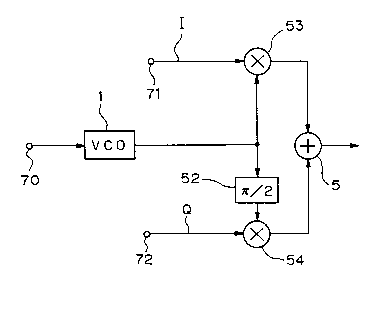
Referring to Figure 1, a quadrature modulation circuit embodying
5 the present invention is shown. In the figure, the same or similar constituents
to those of the conventional circuit are designated by the same reference
numerals, and a detailed description will be omitted to avoid redundancy. As
shown, the modulation circuit has two mixers 53 and 54, an adder 5 for adding
the outputs of the mixers 53 and 54 to produce a predetermined signal, input
terminals 71 and 72 respectively connected to one input of the mixer 53 and
one input of the mixer 54, and a VCO 1 connected to the other input of the
mixers 53 and 54. An analog signal or a digital signal is applied to each of the
input terminals 71 and 72. The VCO 1 has an input terminal 70 and produces
a carrier wave or a FM (Frequency Modulation) wave in response to an input
signal. A nl2 phase shifter 52 is connected between the VCO 1 and one of the
mixers 53 and 54, and rendered conductive in an analog mode.
In operation, when a signal for frequency modulation is received
in an analog mode, it is applied to the input terminal 70 of the VCO 1 to be
modulated in frequency thereby. The resulting FM signal is fed to the mixer 53
20 and Irl2 phase shifter 52. A fixed voltage is applied to each of the input
terminals 71 and 72. As a result, the modulation circuit produces an analog FM
signal. Assume that the received signal is a signal for a quadrature modulation.
Then, if the analog signal input to the input terminal 70 of the VCO 1 is fixed,
the VCO 1 produces an output in the form of an unmodulated wave. Therefore,
208 1 694
when signals I and Q for quadrature modulation are respectively applied to the
input terminals 71 and 72, the modulation circuit produces a digital QPSK
(Quadrature Phase Shift Keying) signal. Specifically, the VCO 1 having the
analog modulation input terminal 70 simultaneously plays the role of the local
5 oscillator 60 (Figure 3) for digital modulation included in the conventional
circuitry, i.e. the two modulators 54 and 65 can be implemented by a single
modulator.
Figure 2 shows an alternative embodiment of the present
invention, which is characterized in that the VCO 1 is included in a frequency
10 synthesizer 20. Specifically, the frequency synthesizer 20 is constituted by the
VCO 1, a 1/N frequency divider 6, a phase detector 7, a charge pump 8, and
a low-pass filter 9. A signal for frequency modulation which is received in an
analog mode is applied to the frequency synthesizer 20, which then produces
an analog FM signal. The analog FM signal is fed to the mixer 53 and nl2
phase shifter 52 while the input signals to the input terminals 71 and 72 are
fixed. As a result, the modulation circuit outputs an analog FM signal. In a
digital mode, the input to the frequency synthesizer 20 will be fixed to produce
a digital QPSK signal in the same manner as in the previous embodiment.
In summary, it will be seen that the present invention provides a
2 o quadrature modulation circuit having a VCO (or a frequency synthesizer
including a VCO) which has an analog modulation capability and replaces a
local oscillator included in a conventional modulation circuit for feeding an
output thereof to a digital modulator. This reduces the number of circuit parts.
An oscillator is no longer needed. Moreover, since an analog modulator and a
r~
~ ~ .
- 208 1 694
digital modulator are implemented in a single modulator, the circuit of the
invention does not require high-frequency switching.
Various modifications will become apparent to those skilled in the
art from reviewing the teachings of the present disclosure. Such modifications
5 are intended to be within the scope of the invention.
. .