Note: Descriptions are shown in the official language in which they were submitted.
2082608
BACRGROUND OF THE lNv~NlION
The invention relates to a telephonic switching network for
selectively switching time division multiplexed digital channels
carrying pulse code modulated voice data and signaling data.
In a conventional telephonic switching network, a central
control processor is made aware of several events needed by it to
correctly establish, maintain and terminate communications
between two parties, or two transceiving units, of the network.
For instance, the central control processor must be informed when
one unit picks up the handset of his phone, or otherwise comes on
line, in order to return a dial tone. The central control
processor must be informed of the digits that the calling party
selects in order to determine the identity of the called unit.
The control processor must then communicate with other switching
nodes in the telephone network in order to establish a path
between the calling party and the called party. Thereafter, the
control processor must be aware of when one party has hung up, so
as to reallocate resources.
This information is conveyed from each phone or each
switching node, by way of signaling data in the form of signaling
bits which are embedded in and accompany the digitized PCM voice
information or data. Somewhere in the network switch the
signaling data must be read and analyzed. This analysis can be
done either with hardware, software, or a combination of both.
Regardless of the form of this analysis, the results must be
passed on to the central control processor in order for a
response to be generated to each signaling data event.
There are two possible modes of operation of a network
switch: cross connect (without signaling data analysis) and PBX
(with signaling data analysis). In the cross connect mode of
operation of a network switch known, the control processor of the
switch is not responsible for formulating or interpreting the
signaling data of each channel. Instead, the central processor is
2082608
only responsible for establishing connections between channels,
while the signaling data is passed without alteration. Other
circuitry in the network ensures the integrity of signaling data
information as it passes from an incoming channel to an outgoing
channel.
In the PBX mode of operation, on the other hand, the
signaling data of incoming channels is terminated at the switch
and interpreted by the control processor of the switch, and then
new signaling data is formulated by the control process and
embedded in the PCM data of outgoing channels. Disadvantageously,
in known multichannel network switches, channels can only operate
in the cross-connect mode or the signaling data analysis mode,
but not selectively in either mode on a channel-by-channel basis.
Such network switches therefore suffer from structural
inflexibility and inefficiency in the handling of signaling
information.
The information conveyed to and from the switch via the
signaling data can be in a variety of formats. The format
employed on a given channel is a function of the type of
telephone equipment which is connected to the switch on the
associated port. In known multichannel switches, the control
processor is not provided with hardware of sufficient versatility
to be able to completely identify transitions of incoming channel
signaling states of each signaling format selectable on a
channel-by-channel basis. This results in considerable
inflexibility for signaling data handling and require substantial
processing power for signaling data operations.
Signaling data must be handled in virtually every network
switch. In some of the known network switches, special circuits
or hardware devices have been employed for identifying
transitions of the signaling state of incoming channels which
serves only a relatively few channels, and the results of
signaling data analysis from each such special circuit are then
conveyed to a control processor. Servicing of several hundreds of
channels in known network switches requires the presence of at
2082608
least one or both of several different, special hardware devices
and several processing entities. However, each of the special
hardware devices employed are restricted to only one type of
signaling information for which they are designed, or they do not
completely identify signaling transitions. Circuit and processor
entities must be replicated multiple times to service a set of
several limited channels resulting in a large number of
distributed components and high cost. Cross connect features are
not found in such general switching products.
SUMMARY OF T~E lNv~NlION
It is, therefore, the principal object of the present
invention to provide a telephonic switching network or network
switch which overcomes the aforementioned limitations of known
networks to achieve enhanced versatility and reduced complexity
and cost. Preferably, channels are selectable for operation in
either cross connect mode or PBX mode of operation on a channel
by channel basis, and signaling data analysis is performed on the
PBX selected channels according to different signaling formats
preselected on a channel by channel basis. Transitions of
incoming channel signaling states are completely identified to a
microprocessor. A plurality of relatively lower order
microprocessors are used for signaling data analysis of channels
associated therewith to convey messages representative thereof
directly to a central control processor for control of switching
of the channels associated with all of the relatively lower order
microprocessors. Each of these lower order microprocessors and
associated hardware elements can serve a large number of
channels, resulting in a cost efficient implementation.
Specifically, it is an object to provide a telephonic
switching network with means for receiving a plurality of time
division multiplexed input channels of incoming information from
selected nodes of the network in the form of PCM voice data with
embedded signaling data, means for preselecting individual ones
2082608
of said plurality of channels for alternative cross connect
treatment and signaling data analysis treatment on a channel-by-
channel basis, and a controllable incoming switching circuit with
signaling data passing capability for passing the incoming
information of each channel for transmission to other selected
nodes in the network selectively with and without embedded
signaling data depending upon the preselection of each incoming
channel for alternative cross connect treatment and signaling
data analysis treatment, respectively.
It is also an objective of the invention to provide a
telephonic switching network with means for receiving on a
plurality of time division multiplex channels of selected nodes
of the network data including PCM voice data and signaling data
on a plurality of channels in a plurality of different
preselected signaling formats, means including a multichannel
incoming switching circuit connected with the receiving means for
switching the data of said plurality of channels to other nodes
of the network, and means for controlling the multichannel
incoming switching circuit to switch said plurality of channels
in accordance with the signaling data in said plurality of
different signaling formats including a multichannel signaling
control circuit responsive to said signaling data and to a state
machine associated therewith for analysis of said signaling data
on each channel according to the signaling format preselected for
each of said channels.
Further, an objective of the invention is to provide a
telephonic switching network with a plurality of multichannel
incoming switching circuits, a central control processor for
controlling the plurality of multichannel switching circuits to
switch a selected plurality of incoming time division multiplex
channels of PCM voice data to a plurality of selected outgoing
channels, means including a plurality of relatively lower order
processors respectively associated with said plurality of
multichannel switching circuits for analyzing signaling data
embedded in the voice data from the incoming channels, means for
2082608
transmitting messages representative of said analysis of the
signaling data from each of the plurality of relatively lower
order processors directly to the central control processor, said
central control processor being responsive to said transmitted
messages for controlling the switching of the channels of all of
said plurality of switching circuits.
In the preferred embodiment, a simple combinational logic
circuit is employed for signaling bit passing on circuit cards
which connect directly to twenty-four channel DSl lines. A 768
channel switching complex is provided with the ability to pass
signaling bits undisturbed by any gain or attenuation elements
which affect voice data, and a state machine based circuit with a
microprocessor is provided for signaling bit analysis on all 768
channels. With this structure, the need is eliminated for
processing entities for groups smaller than 768 channels to be
involved with the signaling bit analysis process to substantially
reduce the number of components required for this function.
Preferably, the multichannel switch is embodied in a single
integrated circuit with means for performing both PBX and cross-
connect functions selectively on a channel-by-channel basis. The
use of a state machine for signaling bit analysis gives the
flexibility needed to handle signaling information from a variety
of different types of channel termination equipment, with the
type selectable on a channel-by-channel basis. The ability to
handle all major commercial signaling formats is preferably
provided together with any proprietary formats which may be
preferred.
State machine based signaling control hardware isolates new
events from the large set of received signaling information. This
enables the use of a relatively lower order processor, since the
hardware needs to be periodically scanned for indications of only
new events. Excessive processing power, which would otherwise be
needed to view the entire set of received signaling information
to determine new events, is eliminated. Alternatively, use of
state machines for this purpose enables use of more cost
2082608
effective processing elements and an increase in speed of the
call set-up and tear-down process.
BRIEF DESCRIPTION OF THE DRAWINGS
The foregoing objects, features and advantages will be
discussed in detail and other objects, features and advantages
will be made apparent from the following detailed description of
the preferred embodiment which is given with reference to the
several figures of the drawing, in which:
Fig. 1 is a functional block diagram of the preferred
embodiment of a telephonic switching network constructed in
accordance with the present invention;
Fig. 2A is a functional block diagram of the incoming
interface circuit block and the incoming multichannel signal
analyzing switching circuit of Fig. l;
Fig. 2B is a functional block diagram of the outgoing
interface circuit block and the outgoing multichannel signal
generating switching circuit of Fig. l;
Fig. 3A is a functional block diagram of a telephonic
network in which the preferred embodiment of the invention is
employed;
Fig. 3B is a detailed schematic diagram of a preferred form
of the digital port circuit of Fig. 3A incoming interface circuit
36 of Fig. 2A and outgoing interface circuit 54 of Fig. 2B;
Fig. 4A is a schematic diagram of the network link interface
circuit 50B of Fig. 3;
Fig. 4B illustrates the preferred network link format
employed with the network link interface of Fig. 4A;
Fig. 4C shows the preferred message format employed with the
network link interface of Fig. 4A;
Figs. 5A, 5B and 5C illustrate the contents of signaling
control registers for individual channel control of signaling as
described with reference to the incoming interface circuit 36 of
2082608
Fig. 2A;
Figs. 6A, 6B and 6C illustrate the contents of registers for
individual channel control of signaling with reference to the
outgoing interface circuit 54 of Fig. 2B;
Fig. 7 is a functional block diagram of a preferred
integrated circuit implementation of the signaling control of
Fig. 2A and referred to as the ABSB IC;
Fig. 8 illustrates the 24 frame organization of the serial
input to the ABSB IC containing time division multiplexed
signaling bits from each of the 772 channels;
Fig. 9 illustrates the organization of the data structures
state RAM of Fig. 7;
Fig. 10 illustrates the data structures of each of the five
types of state RAM elements for the state RAM of Fig. 7;
Fig. 11 shows the four bit commands understood by the ABSB
IC of Fig. 7;
Fig. 12 shows the command execution sequence of the
microprocessor of Fig. 7;
Fig. 13 illustrates the organization of the state RAM of
Fig. 7;
Fig. 14 depicts the timing attributes of a preferred RAM
used in the ABSB IC of Fig. 7;
Fig. 15 shows the register bit definitions for the status
register (read only) of Fig. 7;
Fig. 16 shows the register bit definitions for the response
register (read only) of Fig. 7;
Fig. 17 shows the register bit definitions for the trunk
FIFO register #1 (read only) of Fig. 7;
Fig. 18 shows the register bit definitions for the trunk
FIFO register #2 (read only) of Fig. 7;
Fig. 19 shows the register bit definitions for the trunk
FIF0 count register (read only) of Fig. 7;
Fig. 20 shows the register bit definitions for the special-B
FIF0 register #1 (read only) of Fig. 7;
Fig. 21 shows the register bit definitions for the special-B
20~2608
FIFO register #2 (read only) of Fig. 7;
Fig. 22 shows the register bit definitions for the special-B
FIFO count register (read only) of Fig. 7;
Fig. 23 shows the register bit definitions for the command
register (read/write) of Fig. 7;
Fig. 24 shows the register bit definitions for the command
parameter register #l (read/write) of Fig. 7;
Fig. 25 shows the register bit definitions for the command
parameter register #2 (read/write) of Fig. 7;
Fig. 26 shows the register bit definitions for the backplane
I/O delay register (read/write) of Fig. 7;
Fig. 27 shows the register bit definitions for the error
control register (read/write) of Fig. 7;
Fig. 28 shows the register bit definitions for the ABSB IC
support ROM configuration;
Fig. 29 shows the register bit definitions for ABH, ABL ROM
connections;
Fig. 30 shows the register bit definitions for the overview
of A-only signaling debounce;
Fig. 31 shows the register bit definitions for the state
diagram of A-only signaling debounce;
Fig. 32 shows the register bit definitions for the overview
of AB signaling debounce;
Fig. 33 shows the register bit definitions for the state
diagram of AB signaling debounce - branch 00;
Fig. 34 shows the register bit definitions for the state
diagram of AB signaling debounce - branch 01;
Fig. 35 shows the register bit definitions for the state
diagram of AB signaling debounce - branch 10;
Fig. 36 shows the register bit definitions for the state
diagram of AB signaling debounce - branch 11;
Fig. 37 shows the register bit definitions for the overview
of ABCD (ESF) signaling debounce;
Fig. 38 shows the register bit definitions for the state
diagram of ABCD (ESF) signaling debounce;
2082608
Fig. 39 shows the register bit definitions for the state
diagram of ABCD (ESF) signaling debounce;
Fig. 40 shows the register bit definitions for the state
diagram of ABCD (ESF) signaling debounce;
Fig. 41 shows the register bit definitions for the overview
of ABAB (SLC96) signaling debounce;
Fig. 42 shows the register bit definitions for the state
diagram of ABAB (SLC96) signaling debounce;
Fig. 43 shows the register bit definitions for the state
diagram of ABAB (SLC96) signaling debounce;
Fig. 44 shows the register bit definitions for the state
diagram of ABAB (SLC96) signaling debounce;
Fig. 45 shows the register bit definitions for SBH, SBL ROM
connections;
Fig. 46 shows the register bit definitions for the overview
of special-B signaling decoding;
Fig. 47 shows the register bit definitions for the state
diagram of special-B signaling decoding; and
Fig. 48 shows the register bit definitions for the state
diagram of special-B signaling decoding.
DETAILED DESCRIPTION
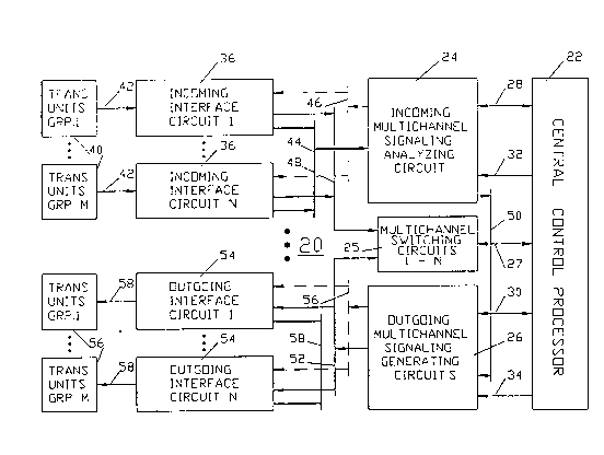
Referring now to Fig. 1 of the drawing, the preferred
embodiment of the telephonic network 20 is seen to include a
central control processor 22 for controlling the switching
operations of one through N, substantially identical, incoming,
multichannel, switching circuits 25. The central control
processor 22 also receives inputs in the form of messages from an
incoming multichannel signaling analysis circuit 24 via an
interface 28. Based on these messages, the central control
processor 22 specifies the connections between channels in the
switching circuits 25 via an interface 27. The central control
processor 22 also directs the outbound signaling of outgoing
channels by providing messages to an outgoing multichannel
2082608
signaling generating circuit 26 via an interface 30.
Each of incoming multichannel signal analyzing circuits 24
has associated therewith a plurality o~ substantially identical
incoming interface circuits 36 connected with a first group of
transceiving units 40 via incoming DSl lines 42. The DSl lines 42
each carry twenty-four time division multiplex channels of pulse
code modulated, or PCM voice data and associated signaling data.
Likewise, each of the outgoing multichannel signaling generating
circuits 26 has associated therewith a plurality of substantially
identical outgoing interface circuits 54 connected with a second
group of transceiving units 56 via outgoing DSl lines 58.
Preferably, there are thirty-two transceiving units groups
for each incoming multichannel signaling analyzing circuit 24 and
multichannel switching circuit 25, and thus each signaling and
switching circuit is capable of handling a total of 768 incoming
channels. The central control processor 22, in turn, is capable
of handling all the channels associated with four or sixteen
incoming multichannel signaling analyzing circuits 24 for a total
of 3072 or 12,288 incoming channels. Each of the incoming
interface circuits 36 interfaces with its associated incoming
multichannel signaling analyzing circuit 24 by an incoming
signaling information bus 44 and an incoming message bus 46. They
are connected to the multichannel switching circuit by an
incoming voice, a communication bus 48 with imbedded signaling.
These busses 44, 46 and 48 each comprise only a pair of wires on
which the information conveyed thereby is time division
multiplexed.
The incoming interface circuits 36 receive messages from the
associated incoming signaling circuits 24 on the message bus 46.
These messages indicate which, if any, of the channels have been
preselected for cross connect treatment (in which signaling data
does not terminate at the incoming signaling circuit 24 and is
not analyzed) or for PBX, or signaling analysis, treatment (in
which the signaling data does terminate at the incoming signaling
circuit 24 and is analyzed).
2082608
11
The incoming signaling data which is embedded in the PCM
voice signal at input 42, is reproduced alone on an incoming
signaling information TDM network link, or incoming signaling
information bus, 44 by the associated incoming interface circuit
36 and provided to the incoming multichannel signaling analyzing
circuit 24. This signaling on incoming signaling information bus
44 is used by the incoming signaling analyzing circuit 24 to
monitor the channels preselected for cross connect and is
analyzed to determine outgoing signaling for channels preselected
for PBX treatment.
The incoming voice communication TDM network link, or bus,
48 carries PCM encoded voice data received at each of the
incoming interface circuits 36. In the case of cross connect
treatment, the incoming PCM voice data is outputted onto the
incoming voice communication bus 48 with the embedded signaling
data intact. When a channel is selected for cross connect
treatment, the embedded signaling data is passed to the
associated switching circuit 25 and treated thereby the same as
the PCM voice data. The incoming voice data with embedded
signaling data from all channels is passed to the switching
circuit 25. The switching circuit 25 passes the PCM voice data
with embedded signaling data from the selected incoming interface
channels 36 via an outgoing voice TDM network link, or bus, 52
carrying voice and message information to each of a 1 - M of
substantially identical, outgoing interface circuits 54. Each of
the outgoing interface circuits 54 has an input connected to an
outgoing message TDM network link,or bus, 56 for receiving
messages from the outgoing multichannel signaling generating
circuit 26. Each of the outgoing interface circuits 54 also has
an output connected to an outgoing signaling data bus 58.
Outgoing signaling data is provided to each of the associated
outgoing interface circuits 54 on the outgoing signaling data TDM
network link, or bus, 58.
Each of the outgoing interface circuits 54 provide PCM voice
data with embedded signaling data to their associated time
2082608
12
dimension multiplexing DSl line 58. In the case of channels
selected for cross connect treatment, the embedded signaling data
is the same signaling data originally received at the incoming
interface circuit 36, while in the case of channels selected for
PBX, or signaling analysis treatment, the signaling data is
generated by the outgoing, multichannel, signal generating
circuit 26. It should be appreciated that the DSl interface
circuits of both the incoming interface circuits 36 and the
outgoing interface circuits 54 contains a single device
functioning as a transmitter of data on the twenty-four channel
DSl line from the lines 58 and as a receiver of data for those
same twenty-four channels arriving at the switch on DSl lines 42.
Referring to Fig. 2A, the details of the incoming interface
circuits 36 and the incoming multichannel signal analyzing
circuit 24 of Fig. 1 are shown as implemented in the preferred
embodiment. Each of the incoming interface circuits 36 is
preferably implemented on a separate twenty-four channel DSl Port
Card. The twenty-four channels of PCM encoded voice with embedded
signals carried on incoming DSl line as is applied to an input of
an interface and buffering circuit 60 which connects the incoming
digital signals to appropriate levels for processing, buffers
them in a series of registers and extracts a separate copy of
signaling data from the PCM with embedded signaling and provides
it on line 61. The voice data with embedded signaling voice data
is applied to an input 62 of a signal controller 64. The
extracted signaling data on line 61 is provided to an input 66 of
the signal controller 64 and also to the incoming signaling data
TDM networ~ link 44. PCM voice encoded data with embedded
signaling data is generated on an output 68 by the signal
controller 64 which, in turn, is connected to incoming voice
communication bus 48.
Signaling information on DSl lines is conveyed as the least
significant bit of the eight bit PCM data of each channel in
specially designated frames of the superframe structure defined
for the DSl interface. The multichannel switching circuit, or
2082608
13
switch 25 likewise utilizes the same superframe structure with
specially designated signaling frames, though, there is no
inherent phase synchronization between the incoming DSl line
superframe structure and that of the switch 25. The interface and
buffering circuit 60 will provide an alignment of at least the
frames, if not necessarily the superframes, of the asynchronously
arriving DSl line and the switch 25. The voice with imbedded
signaling data output 62 of the interface and buffering circuit
60 will therefore not necessarily contain signaling data in the
least significant bit of PCM data in those frames which the
superframe structure of the switch has designated signaling
frames. The signaling buffer portion of the interface and
buffering circuit 60, however, will copy the signaling data
received from the incoming DSl line 42, store it, and convey the
signaling data on line 61 and input 66 aligned to the switch 25
in accordance with the superframe structure of the switch 25
which designates the specific signaling frames. The
synchronization function provided by the interface and buffering
circuit 60 is necessary for all signaling operations within the
switch 25 and, with the method employed in this invention,
provides for a range of potential signaling treatments.
A relatively low processing power processor, or low power
processor 70, preferably a type 68008 made by Motorola, in
response to incoming messages at 46 applied to input 72,
indicates to the interface circuit 60 the type of DSl line
present via an output 74 of the low power processor 70. A
selection is made between two types o commercial DSl service: D4
and ESF. Selection of DSl line type is an initialization
function, dictating the standard types of interface and signaling
buffering functions required.
The low power processor 70 selects for each one of the
twenty-four incoming channels one of three types of treatments or
modes: DSl crossconnect treatment, DS0 crossconnect treatment, or
PBX (also referred to as signaling analysis) treatment. As
indicated, the interface and buffering circuit 60 has two types
2082608
14
of twenty-four channel time-division multiplexed outputs: channel
voice with imbedded signaling data on input 62 and a copy of the
channel signaling data on line 61 and input 66. Inputs 62 and 66
of the signal control circuit 64 from the incoming interface and
buffering circuit 60 will be identical for channels in any of the
three modes of signaling treatment and are a function of the type
of DSl line service employed at 42.
Output 68 from the DSl port card 36 is formulated using the
signaling control circuit 64 which is programmed specifically for
each channel via a signal 76 from central control processor 22
as a function of the desired type of signaling treatment.
Channels programmed via signals at 76 for operation with
either DSl crossconnect mode or PBX mode will be treated
identically by the signaling control circuit 64. The signaling
control circuit 64 will allow the voice data with imbedded
signaling received at input 62 to pass undisturbed to output 68.
As previously noted, the imbedded signaling data at input 62 will
not necessarily be aligned to the superframe structure designated
specific signaling frames of the switch. However, the other
elements of the switch 25 will treat the data output on 68
distinctly for DSl crossconnect mode and PBX mode.
Channels programmed via a signal at 76 to operate with DS0
crossconnect treatment will force the least significant bit of
PCM data received input 62 to be replaced with signaling data
from input 66 during those frames designated by the superframe
structure of the switch as signaling frames on output 68. In this
fashion, PCM data for each channel selected for DS0 crossconnect
treatment has signaling bits present in their LSB during the
defined signaling frames. Accordingly, the switch need only
connect the signaling bits to an output channel for transmission
without further interaction for signaling operations.
Independent of the mode of signaling treatment, output 66
from the interface and buffering circuit 60 contains signaling
data for each channel aligned to the superframe structure of the
switch. For channels designated for PBX treatment, this data will
2082608
be terminated by and analyzed at the 768 channel signaling
control circuit 80 of the incoming multichannel signaling
analyzing circuit 24. For channels designated for DS0 or DSl
crossconnect treatment, this signaling data, while not required
for determination of the appropriate outgoing signaling for that
channel, will also be available for monitoring the active/idle
status of each channel by the 768 channel signaling control
circuit 80.
The selection of signaling treatment is an initialization
function. Once set, there are no further communications required
between the incoming interface circuits 36 and any other system
elements regarding signaling operations except to alter the
desired mode of signaling treatment. The minimization of messages
being passed between the switch and the interface circuit
advantageously results in reduced time delay to set up and tear
down connections.
Still referring to Fig. 2A, each of the incoming
multichannel signal analyzing circuits 24 is preferably in the
form of a 768 channel switching and signaling control circuit
including a medium processing power, or medium power, processor
78, and a 768 channel signaling control circuit 80 with one or
more associated hardware state machines such as a commercial
signaling state machine 82 (capable of handling the structural
termination types AB, SLE96 and BSF) and a proprietary signaling
state machine 84 (capable of handling any special signaling
formats). Preferably, the switching circuit 25 is comprised of a
768 channel switching element with signaling data passing
capability, or switching element, 86. The medium power processor
78 preferably comprises a type 68000, made by Motorola. The
preferred embodiment of the signaling control unit 80, the state
machines 82 and 8 and the switching element 86, are shown in and
will be described in detail with reference to Figs. 3, 4A, 4B and
4C, 5A, 5B and 5C and 6, and other drawing figures, but their
general function will be first described briefly here.
The signaling control circuit 80 receives the incoming
- 2082608
16
signaling data at an input 88 and compares and analyzes the
signaling data in accordance with one or more signaling formats
according to algorithms stored in hardware state machines 82 for
different commercial signaling formats and according to an
algorithm stored in proprietary state machine 84. Those state
machines are preferably embodied in the form of EPROMs, such as
any standard 32K x 8 EPROM made by TI, Intel or others.
In keeping with one aspect of the invention, the EPROMs are
preferably mounted for releasable connection to facilitate
changing of the algorithms associated with the different
signaling formats. A proprietary signaling format of proprietary
state machine 84 can be provided on some channels, while other
channels employing standard signaling formats are selected on a
channel by channel basis or are given cross connect treatment.
The medium power processor 78 receives messages on message
bus 28 from the central control computer 22 including messages
concerning which signaling format is to be used with which
channel for channels selected for signaling data analysis
treatment. The medium power processor 78 conveys this information
in the form of selection signals on line 90 to the signaling
control circuit 80. In turn, the signaling control circuit 80
conveys on line 90 to the medium power processor 78 signals which
indicate which of the channels have had a change in status of the
signaling data. This status change information is interpreted by
the medium power processor 78 and thereafter is conveyed to the
central control processor 22. The central control processor 22
responds by making specific channel connections in the line
switching circuit 86 via a line 32 applied to an input 92. The
switching circuit 86 responds to the switching control signals at
input 92 to appropriately control the switching circuits 25 to
switch the incoming communication from bus 48 which is applied to
the outgoing interface circuits 54 via network link 52. Channel
data output applied to 96 from the switching element 86 comes
from 768 channel node of the incoming interface circuits 36 or
from other 768 channel switching nodes.
2082608
17
Referring now to Fig. 2B, the outgoing interface circuit 54
and outgoing multichannel signal generating switching circuits 26
are seen to be comprised of elements which parallel those of the
incoming interface circuits 36 and the incoming multichannel
signal analyzing circuit 24, respectively. In fact, much of the
corresponding incoming and outgoing circuits can be implemented
partly, or completely, in the same semicustomized circuits.
In any event, the incoming channel data appearing on the
channel data bus 52 from a channel data output of the
multichannel switching circuit 86, Fig. 2A, is received as
outgoing channel data. The switching circuit 102 has an input 104
for receiving the switching control signals from the outgoing
switching control signal output 27 of the central control
processor 22, Fig. 1. Based on these switching control signals at
an input 100, the switching circuit 102 appropriately switches
outgoing channel data at input 100 through to its output 106 and
the outgoing channel data bus 52.
In the case of cross connect channels, the signaling data
switched through the outgoing switching circuit 102 is embedded
in the voice data. For a channel selected for signaling bit
analysis, on the other hand, the signaling data has been removed
and is separately generated by an outgoing multichannel signaling
control circuit 108. The control circuit 108 preferably capable
of handling the same 768 channels corresponding to the incoming
channel signaling control circuit.
The outgoing channel signaling control circuit 108 produces
outgoing signaling data on its output 110 according to different
signaling format data specified by a medium processing power
processor, or medium power processor, 116 such as a 68000 made by
Motorola, or the like. Selection of the signaling format for each
channel by the signaling control circuit 108 is based on messages
from an output 109 of the medium processing power processor, or
medium power processor, 116. Preferably, the processor 116 is the
same processor as processor 78, Fig. 2A. The medium power
processor receives input messages from the central control
2082608
processor 22 at a message output 30. It transmits messages to the
outgoing message bus 56 in addition to conveying messages to the
signaling control circuit 108 on a separate output 109. Likewise,
the outgoing signaling data on output 110 feeds the outgoing
signaling data bus 58.
Each of the outgoing interface circuits 54 is seen to
include a low processing power, or low power, processor 118, a
signal controller 120 and an interface and buffering circuit 122
corresponding to the processor 70, a signaling controller 64 and
an interface and buffering circuit 60, respectively. Each of the
signaling controllers 120 has an input 124 coupled to the channel
data bus 52, and each of the lower power processors 118 has an
input 126 coupled to the message bus 56. Each of the signaling
controllers also has an input 128 connected to the signaling data
bus 58. Preferably, processors 36 and 54 are embodied in the same
device performing all the different functions.
Depending upon a message received at input 126, the low
power processor transmits control signals on outputs 130 and 132
to the signal controller 120 and the interface and buffering
circuit 122, respectively, to cause a channel to be treated as a
cross connect channel or a signaling data analysis, or PBX,
channel. If a channel is selected for cross connect treatment,
the channel data will already contain signaling data, and this
composite signal will be passed by the signal controller 120 to
the interface and buffering circuit 122 without insertion of
signaling data from the signaling control circuit 108. The
interface and buffering circuit 122 receives a command from
processor output 132 which causes it to pass the composite signal
to the outgoing DSl line 58 without buffering.
If, on the other hand, a channel has been selected for PBX
treatment, a command signal on processor output 130 causes the
signal controller 120 to embed the signaling data at input 128
into the outgoing channel data at input 124 to form a composite
signal on its output 134 containing embedded signaling data
generated by the signaling control circuit 108. The signaling
2082608
contEol circuit causes the appropriate signaling data in exactly
the format and content 6pecified by the outgoing signaling
circuit 26 to be sent to th~ DSl lin~ 58. Th~ ~p~c~flcation by
command signal on bus 56 from the outgoing signaling control
circuit 26 to the outgoing signaling circuits 54 to indicate the
desired mode of signalinq treatment for each channel is done only
at initialization. No other messages are required between these
entities for control of signaling operations except to change the
mode of treatment.
Still referring to Figs. 2A and 2B, in the preferred
e~bodiment there is a hierarchy of board-level components with
each DSl port card 36 and 54 being at the lowest level and
serving only twenty-four channels. Then switching and signaling
control nodes are in the middle and serve 768 channels, while the
central control processor is at the highest level serving all
channels from a plurality of the switching and signaling control
nodes. In other architectures, the channelization at each level
in the hierarchy may be different and, in fact, the number of
levels in the hierarchy could vary, but the structure is believed
to represent the optimum levels in the hierarchy and the optimum
channelization for each level in the hierarchy. The signal
handling components have been located advantageously. The signal
control circuit 64 is at the lowest level card or block in the
hierarchy. The function is simply to embed signaling information
into the voice data on a channel-by-channel basis or to avoid
disturbing the voice bits. As noted above, the specification of
"replace or don't replace" need happen only during switch
initialization and represents the only interaction that the
processors 70 need have in the signaling handling process. This
enables use of very low processing power microprocessor on the
most prevalent type of card in the entire system. This is enabled
because there is a separate path on buses 44 and 58 for
connecting signaling information between the port cards to the
768 channel signaling control circuits 80. It ~hould al~o be
noted that the voice or voice with embedded signaling data flows
19
2~82608
directly into a switching node.
Likewise, at the 768 channel switching and signaling control
node, or module, 24 the signaling information for all 768
channels is analyzed by the signaling control circuit 108. New
events are identified by this circuit in cooperation with the
state machines 112 and 114 and are passed to the processor 116
for further action. This processor 116 will communicate only this
necessary information to the central control processor to obtain
the appropriate signaling response and switching activity and,
thus, only use of a medium power processor is all that is
required in the middle of the hierarchy of modules or cards.
Because the signaling control circuit 108 is supported by state
machines 112 and 114 a wide variety of signaling formats - any
number of different channel types (and their associated signaling
formats) can be employed concurrently in the switch and all will
be serviced by the same circuitry.
When data is returned to the appropriate port card 54 for
outbound transmission, again a small logic circuit is employed to
choose the source of signaling bits which are to be transmitted
to the outbound DSl line from the 768 channel signaling control
circuit 108 or from the voice with embedded signaling provided at
switch 108. Again, this selection is needed to be made on a
channel-by-channel basis only once at power-up time, and
processor 118 must take for signaling handling.
The messages passed to the central control processor 22 are
from the N processors 78 or 116 of the switching and signaling
control modules 24 and 26, respectively, such that there are no
intermediaries in these communications and faster operation is
obtained. Specifically, there is no need for the central control
processor to interact (after the power-up sequence) with the 32xN
DSl port cards 36 and 54 for the purpose of signaling handling.
For pure PBX operations there would be no need to have the
signal control circuits 64 and 120 on the port cards 36 and 54
and no need for signaling passing capability through the
switching elements 86 and 102. For pure cross-connect operation,
2082608
there would be no need for the signaling control circuits 80 and
108 and then associated state machines 82, 84, 112 and 114 and
located together with the switching elements 86 and 102. By
providing this optimized circuitry, the switching network has the
flexibility and to function not only as a PBX system or only as a
cross-connect system, but to simultaneously function as both
types of systems. This flexibility has been achieved with
minimal circuit complexity and cost through means of the
hierarchial structure described above.
Referring now to Fig. 3A, the preferred embodiment of the
invention is preferably employed to interface with various
elements of a network subsystem 229 which, in turn, is connected
with an SBX bus 230 of a control subsystem and the elements of a
network termination subsystem. Communication of the elements of
the subsystem with a central controller and a central memory (not
shown) of the telephonic switching system is through means of an
SBX bus 230. The control subsystem of bus 230 is preferably a
68020/68030 microprocessor based multiprocessor, distributed
processing system which is capable of either simplex or duplex
operation. The network subsystem 229 consists of a system clock,
or CLK, 232 and four interactive switching/control modes (only
two shown), each comprising a single stage, nonblocking, 772
channel time slot interchanger, or TSI, 234. Most of these
channels (768) are broken down into thirty-two groups of twenty-
four channels for interface over high speed serial interfaces
known as network links to transition circuits of the network
termination subsystem 227. A network shelf controller, or NSC,
circuit 236 connected to the TSI 234 has a 68000 microprocessor
with two Mbytes of DRAM to provide processing capability of
signaling activity on the 768 channels of each switch mode.
Within the NSC circuit 236, the 768 channel parallel time
division multiplexing, or TDM, bus to and from the TSI circuit
(not shown) is multiplexed into a thirty-two, twenty-four channel
3.088 MHz serial links, or network links, to and from the network
termination subsystem 227. The TSI circuit 234 provides access
2082608
to higher level processing for itself and the NSC circuit 236 via
an SBX interface (not shown) to an SBX circuit residing on the
control subsystem secondary bus 230. The central controller
memory and central controller are loaded via this secondary bus
230.
The circuits which form the network termination subsystem
227 include a DAS, or digital audio source, 237 for providing
tones, announcements and messages; a basic rate line, or BRL,
circuit 238; a primary rate interface circuit, or PRI, 240; one
or more DS1 port circuits 242; and a digital signal processing,
or DSP, circuit 244. The BRL circuit 238 provides system access
to agent and supervisor consoles, while the PRI circuit 240
provides termination of the twenty-fourth 64 Kbit channel of the
TI digital trunk and also has all the features of a DS1 port
circuit 242. The DSl port circuit 242 provides digital Tl trunk
access into the system. PCM channels are appropriately formatted
and delivered to a DS1 transmit link 246. Incoming information
from the DS1 link 246 are recovered, buffered and delivered to
network links for access to the network. The digital signal
processing circuit 244 provides three separate TMS 320C25 digital
signal processor based circuits for accessing eight of the
twenty-four system channels that the DSP circuit 244 accesses
over its link into the network. The DSP 244 processor receives
functions for MF and DTMF signals and can also be used for tone
metering functions in system diagnostics. As seen,
advantageously a linkage 247 of only four wires connects each of
the elements of the network termination subsystem 227 with the
NSC 236 for a differential system or only two wires in a
nondifferential system.
The wire linkages 247 are made possible by virtue of use of
network link interface, or NLI, integrated circuits 250 of Fig.
3B. The single NLI circuit 250 is capable of operation in
different modes depending upon the application in which it is
employed. One or more NLI circuits 250, operating as network
termination units 250, are contained in each of the network
23 2082608
termination subsystem elements 237, 238, 240, Z42 and 244 of Fig.
3A, and multiple NLI circuits, operating as control units 250 are
contained in the NSC circuit 236 of the subsystem 229.
Preferably, the NLI circuit 2S0 is implemented in a large scale
integrated circuit package having preselected input and output
terminals, although separate integrated circuit packages for each
of the different modes of operation could be provided in lieu of
a single package.
Referring to Fig. 3B, the interface and buffering circuit 60
of Fig. 2A and interface and buffering arm 122 of Fig. 2B is
implemented by means of a combination of these elements, an
elastic buffer lS3, a DS1 transceiver 15Z and a line interface
circuit 151 while the signal control unit 64 of Fig. 2A and
signal control circuit 120 of Fig. 2B are preferably implemented
in a network link interface, or NLI, circuit 50. The details of
the structure of the NLI circuit 50 will be described below with
reference to Figs. 14 through 48. Figs. 30 - 32 relate to per
channel controls of signaling as described above with reference
to the operation of the transmitting DSl port card 54 of Fig. 2B
in which insertion of signaling bits is indicated by a logic-1
while a noninsertion command is indicated by a logic-0. Figs.
33-35 are related to per channel controls of signaling as
described above with reference to the operation of the DSL port
card 36 operating in a receiver mode in which cross connect
treatment is indicated by a logic 1 while PBX . . .
Still referring to Fig. 3B, for purposes of illustration,
the network link interface circuit 250 is shown being used as a
network termination unit, or slave, circuit 250 to interface one
of the DS1 port circuits 242, Fig. 3A, with another network link
interface circuit 250, operating as a control unit, or master
unit, 250.
The DPC 242 provides termination for a single DSl trunk,
interfacing its twenty-four channels into the network. The DPC
242 provides for received DSl clock recovery, framing control,
buffering of received PCM and AB(CD) signaling data, as well as
2082608
24
DSl line performance monitoring. Through the elastic buffer 253,
the received DSl line's PCM and signaling data received on the
DSl line 246 is synchronized with the a system clock appearing on
line 251A. The data read from the elastic buffer 253 is
transmitted on a network link 247 to the network. Information to
be delivered to the outgoing DSl line 246 is similarly received
from the network on a network link 247. The microprocessor
monitors bit-error rate and slip performance of the DSl line,
monitors for alarm conditions, controls loopback and other
diagnostic facilities, and maintains communication with the
control system via a datalink provided in the network link 247.
The received DSl signal from an office repeater bay (ORB),
channel service unit (CSU), or galaxy voice circuit (GVC) port
interface equipment is transformer-coupled and terminated on the
DPC 242, as shown. Similarly, each DSl signal transmitted is
transformer-coupled to the line. Three VLSI devices form the core
of the DSl interface function of the DPC 250: the line interface
unit 251, the DSl transceiver 252, and the elastic buffer 253.
These three VLSI devices are programmable by the DPC
microprocessor 254.
The DPC's line interface unit 251 provides appropriate
termination and line driver circuitry for DSl line interface 246,
in addition to a programmable line build-out function. The line
interface unit 251 also recovers the clock signal on the receive
line 246A, presenting this clock and the 1.544 MHz serial data
thereon to the DSl transceiver 252 on lines 251A and 251B,
respectively. Similarly, the line interface unit 251 will be
provided with 1.544MHz serial data by the DSl transceiver 252 on
line 252A for transmission on the outbound DSl line 246. The
received DSl line clock extracted by the line interface unit 251
may also be output by the DPC 242 for cabling to clock
controlling circuitry of the network (not shown) as a reference
input.
The DSl transceiver 252 locks on to the framing pattern
of the receive DSl line 246A and passes each channel of PCM and
208260~
signaling data to the elastic buffer 253 device. Bit error counts
and alarm conditions of the received DSl line are maintained by
the DSl transceiver 252. Similarly, PCM and signaling data to be
transmitted on the outbound DSl line 246B are provided by the NLI
250 to the DSl transceiver 252 for framing.
The elastic buffer 253 buffers the received PCM and
signaling information for each channel to allow for variations
between DSl line and system clocks. This data is read from the
buffer by the NLI 250 in synchronism with the system clock.
Preferably, the elastic buffer device 253 is programmed to
perform signaling integration and freeze functions, if desired.
The NSC 236 encodes the system clock and synchronization
signals onto the network link 247 and these signals are decoded
by the NLI 250 and its associated phase-locked loop circuitry.
The NLI 250 provides the mechanism for connecting the twenty-four
channels of PCM and signaling data of the DPC 242 with the
network. The NLI 250 also provides the means for the
microprocessor 254 to communicate with the microprocessor of the
NSC 236 over the 768kbps datalink of the network link 247. In
redundant systems, the NLI 250 is connected to an NSC 236 in each
network copy.
The DPC 240 contains a 68008 microprocessor 254 is a 68008IC
operating at six MHz. The major function of the microprocessor
254 is to program the DSl interface circuitry of the NLI SOB and
to monitor the DSl line 240, reporting error and alarm conditions
to the NSC 236. The microprocessor 254 will interact with the NLI
SOB for communication with the NSC 236. In such case, the DSl
transceiver 252 will control the facilities data link 251A in ESF
DSl applications. Alternatively, for remote agent applications,
the NLI 250 will control a datalink to remote facility 257B
maintained in one of the 64kbps channels of the DPC 242.
The DPC 242 contains sixty-four kbytes of no wait-state
EPROM 255 for boot loading and diagnostic code. The DPC 242
contains 32kbytes of no wait-state RAM 256 which can be
optionally expanded to 96kbytes. The RAM 256 can be write-
2082608
26
protected in 8kbyte blocks.
Several registers are also provided in the address space ofthe microprocessor 254 to allow for control and monitoring of
various functions.
The microprocessor 254 can receive interrupts from the NLI
2S0, the DSl transceiver 252, the line interface unit 251, the
serial communications controller 257, and by a ten microsecond
signal developed in the NLI 250.
In order to provide for remote agent capability, the DPC 242
is provided with access to one of the twenty-four sixty-four kbps
channels of the DSl line 246 to facilitate 'D' channel control in
an ISDN '23B+D' environment. The received sixty-four kbps data is
passed by the DSl transceiver 252 through the NLI 250 to a Z8530
serial communications device, or data links 257A and 257B,
controlled by the microprocessor 254. The devices 257 will
serialize the sixty-four kbps data stream and pass this through
the NLI 250 to the DSl transceiver 252 for transmission to the
outbound DSl line 246B. At a remote site, another DPC 242 will be
present as the source and sink of this 'D' channel information.
The DPC accepts redundant -48VDC inputs and contains a DC-
to-DC power converter to derive the +5V required for its logic
circuits.
Referring to Fig. 4A, the NLI 250 has five interfaces: an
outbound data interface, the transmit link interface 282, the
receive link interface 286, an inbound data interface 288, and a
microprocessor interface 290. The outbound data interface 282
provides means for a card to hand off PCM and signaling data to
be transmitted on a network link. This data is merged with
information specified for transmission by the microprocessor
interface 290 and is sent in pulse-width modulation encoded form
to the outbound network link by the transmit link interface 284.
In the other direction, data received form a network link 247
arrives at the receive link interface 86 where PCM and signaling
data is extracted and sent to the inbound data interface 288 for
output from the NLI 250. Message information is also extracted
2082608
27
from the received network link 247 and is routed to the
microprocessor interface 290. The connections between the
microprocessor interface 290 and both the receive and transmit
interfaces 286 and 284 are made via FIFOs 291.
While there are several formats for data flowing across the
NLI inbound and outbound data interfaces 288 and 282, the format
of data on each network link 247, whether created by the transmit
link interface 284 or received at the receive link interface 286,
will always be as indicated in Fig. 4B.
The outbound data interrace 282 will accept either parallel
or serial input for network link transmission. The operation of
the outbound data interface 282 is dependent on the strapping of
the NLI mode select pins.
As stated previously, each of the thirty-two NLI circuits
250 on the NSC circuit 236 receives parallel data for each of
twenty-four channels for network link transmission. This data is
obtained from a 768 channel TD~ bus. Referring to Fig. 4B, each
NLI 250 will latch a set of twenty-four, eleven bit samples at an
approximate 192kHz rate. The timing for this latching is derived
from counters within the NLI 250 which are driven by a 12.352MHZ
control time base clock, and 333Hz synchronization pulse provided
to each element on the NSC circuit 236. To identify which set of
twenty-four channels of the 768 channel bus are intended for a
given circuit, each NLI 250 has a position register loaded with a
value from zero to thirty-one. Each NLI 250 on NSC circuit 236
will have a different value in its position register. The eleven
bits handed to each NLI 250 originate at the TSI circuit 234 and
consist of eight PCM and three system bits. The three system bits
include a parity bit, a frame bit, and a superframe-synchronous
signaling (SFSS) bit. All of these inputs except the SFSS bit are
sourced from the switching complex. The SFSS bit is generated by
the signaling circuit on the TSI circuit 234 and is passed to the
NLI 250 in parallel with the other ten. The parity bit received
by the NLI 250 is on the eight PCM and one frame bit generated by
the TSI 234, and checking of this parity is performed in the
2082608
28
outbound data interface 282, Fig. 4A. If a parity error is
detected, the appropriate bit of an NLI interrupt status
register, will be set and the DPC circuit's microprocessor of the
DPC 242 will be interrupted. Regardless of the priority check
results, the ten remaining data bits are transferred to the
transmit link interface 284.
on DPC circuits 242, Fig. 3A, and PRI circuits 240, serial
PCM and parallel signaling data is received at the outbound data
interface 282 for transmission on a network link 247. The serial
stream contains twenty-four channels of PCM data and a frame bit
is received at a 1.544MHz rate. A pin 292 (not shown) of the NLI
2S0 is provided to source a transmit 1.544MHZ clock for use on
DPC circuits 242 and PRI circuits 240 in generating this data
stream. An eight kHz transmit sync output pin (not shown) is
provided on the NLI 50, so that channel order can be derived on
the NLI 250. Timing of each of t:hese clock signals is derived
from the received network link synchronization information in
conjunction with the 12.352MHZ input to the NLI 250 from the NLI
PLL pin.
The eight bit PCM sample of each channel is extracted from
the received serial stream and is converted into parallel form.
The frame bit of the serial stream is latched and passed in
parallel with the parallel PCM data of each channel to the
transmit link interface 284. The four bits of signaling
information received at the outbound data interface 282 represent
the A, B, C, and D signaling bits for each channel. Based on
system-defined superframe timing, the appropriate signaling bit
of the four received is selected and sent to the transmit link
interface 282 in parallel with the PCM and frame bits. Under
microprocessor control, this signaling data may also be specified
to replace the LSB of outgoing PCM samples. This type of control
is maintained on a channel-by-channel basis through processor
specifications for each channel in the transmit signaling control
registers.
Operation of the outbound data interface 282 is comparable
2082608
29
on BRL circuits 238, except that no signaling bits are passed to
the NLI 250.
On DAS circuits 237, twenty-four eight bit parallel PCM
samples are presented to the outbound data interface 282 every
125 microseconds for transmission to a network link. The NLI 250
will supply the DAS 237 with an eight kHz transmit sync output on
pin 293 to be used with the on board 12.352MHz clock such that
the timing and channel order for passing data to the outbound
data interface 282 can be derived. The DAS circuit 237, will
supply the NLI 250 with data for transmission at a 192kHz rate.
This data will, in turn, be transferred to the transmit data
interface 284.
On DSP circuits 242, serial PCM data is received at the
outbound data interface 282 for transmission on a network link
247. The serial stream contains twenty-four channels of PCM data
and is received at a 1.536MHz rate. The 1.536MHz transmit clock
pin 295 of the NLI 250 has been provided to source the clock to
be used on the DSP circuit 244 in generating this data stream.
The eight kHz transmit sync pin 293 is also used for determining
channel order. The 8 bit PCM sample of each channel is extracted
from the serial stream, converted into parallel form and passed
to the transmit link interface 284.
The transmit link interface 284 receives data from the
outbound data interface 282 and the microprocessor interface 290.
Sixteen bit data for link transmission is formed by combining the
(up to) ten bits from the outbound data interface 282 with four
bits from the microprocessor interface 290, generating odd parity
on the set, and appending a bit fixed as logic one. Twenty-four
such words are formed every 125usec. Two link sync bits are added
to these twenty-four, sixteen bit words and the entire block of
information is serialized. The setting of the NLI's Master/Slave-
pin 280 determines the coding employed on the outbound 3.088MHz
stream. NLI circuits 250 strapped to function as a master 250
employ a pulse-width modulation coding in order for the NLI
circuits 250 operating as a slave 250 at the far end of the
2082608
network link to be able to derive a clock from the low-to-high
transition which begins each bit interval. NLI circuits 250 which
are strapped as a slave 50B output the 3.088MHz stream as simple
NRZ, the ones represented as high voltages for the entire bit
interval and zeros as low voltages.
The receive link interface 286 receives a 3.088MHz network
link and passes the stream immediately through a decoder.
Transitions of data on the received stream are detected in the
pulse-width modulation decoder, and a 3.088MHz clock is derived.
This clock is divided by two to form a 1.544MHz signal which,
with respect to NLI circuits 250 specified for slave operation by
their Master/Slave-pin 280 setting, will be sent out of the NLI
250 to a phase-locked loop circuit, where 12.352MHz is created
and passed back to the NLI 250 for use in deriving all timing.
The serial data output of the decoder is clocked into a shift
register at a 3.088MHz rate to convert the data into parallel
form. Sixteen bit words are formed in this fashion consisting of
ten bits bound for the inbound data interface 288, four bits for
the microprocessor interface 290, a parity bit on the entire
word, and a fixed bit of logic one. An odd parity checker is used
to verify a properly received data word and, if a parity error is
detected, the appropriate bit of the NLI interrupt status
register, will be set and the microprocessor of the NLI circuit
250 will be interrupted. In the 3.088MHz link there are 386 bits
transmitted every 125 microseconds. Since only 384 are used for
channel data (twenty-four sets of sixteen bit words), two extra
bits of link sync information are also received in the data
stream. These bits are routed to the counter/timer circuit 292,
Fig. 3A, where they are used for acquiring synchronization to the
link transmitter.
The inbound data interface 288 receives ten bits from the
receive link interface 286 and transmits this data in either
parallel or serial form. The mode select pins on the NLI 250 are
used to select the output mode for each card.
On the NSC circuit 236, data from each of the thirty-two
2082~08
31
inbound data interfaces 288 are merged to form a 768 channel TDM
bus. Each NLI master circuit 250 will source a set of twenty-four
eleven bit samples at an approximate 192kHz rate. The timing for
this latching is derived from counters within the NLI circuit 250
which are driven by the 12.352MHZ clock and 333Hz synchronization
pulse provided to each NLI 50 on the NSC circuit 236 by the clock
card 23Z, Fig. 3. Each NLI circuit 250 has a position register
loaded with a value from zero to thirty-one to determine when it
should output to this 768 channel bus. When a given NLI circuit
250 is not outputting data, it will keep its output pins in a
high impedance state. When a given NLI circuit 250 is outputting
data, the EXG pin of that NLI 250 will generate a low level pulse
which is used for special purposes on the NSC circuit 236.
Eleven bits of output are provided by the inbound data
interface 288 of each NLI circuit 250, consisting of eight PCM
and three system bits. The three system bits include a parity
bit, a frame bit and a SFSS bit. All of these outputs except the
SFSS bit are sent to the TSI circuit 234, with the parity bit
generated on the nine non-SFSS data bits. The SFSS bit is sent to
the signaling circuit of the TSI circuit 234 in parallel with the
other ten.
In DPC circuits 242 and PRI circuits 240, serial PCM data is
output by the inbound data interface 288. The serial stream
contains twenty-four channels of PCM data and a frame bit and is
transmitted at a 1.544MHz rate. The receive 1.544MHz clock pin
of the NLI is used by DPC 242 and PRI 240 in latching this data
stream. A 333Hz receive sync output pin 294 has also been
provided such that channel and frame order can be derived on
these circuits. Timing of each of these clock signals is derived
from the received network link sync information in conjunction
with the 12.352MHz input from the NLI phase locked loop circuit.
Signaling information obtained for each channel in the SFSS
bit position on the received network link may be inserted into
the LSB of each PCM word output by the inbound data interface 288
in accordance with the system-defined superframe timing. This is
2082608
32
selectable on a channel-by-channel basis under microprocessor
control by setting the bit corresponding to a channel in the
received link signaling control registers, Figs. SA. SB and 5C.
Operation of the inbound data interface 288 is comparable on BRL
circuits 238, except that no signaling bit information is ever
inserted into PCM samples.
In DAS circuits 237, twenty-four eight bit parallel PCM
samples are output by the inbound data interface 288 every
125usec. Each of the four NLI circuits 250 on the card will be
assigned a distinct value in their position register, to define
when each should present parallel output onto a common output
bus. When a given device is not passing data from its inbound
data interface 288 to this bus, its output pins will remain in a
high impedance state. The DAS circuit 237 circuitry will make use
of a OSYC pin of the NLI circuit 250 to determine when output
data should be latched from a given NLI circuit 250.
In DSP circuits 242, serial PCM data is output by the
inbound data interface 288. The serial stream contains twenty-
four channels of PCM data and is transmitted at a 1.536MHz rate.
The 1.536MHz receive clock pin 292 has been provided to source
the clock to be used on the DSP circuit 244 in generating this
data stream. An 8kHz receive sync pin and the 1.536MHz and 8kHz
pins provided for interaction with the inbound data interface 288
and those provided for interaction with the outbound data
interface 282 are distinct. Each set has a different phase than
the other. The eight bit PCM sample of each channel is extracted
from the serial stream, converted into parallel form and passed
to the transmit link interface 84.
For channels received by the DSP circuit 242, signaling bits
are present in the LSB of PCM samples during the system-defined
signaling frames. A-signaling bits will be captured by the NLI
circuit 250 and stored in the receive signaling data registers,
Figs. 36 - 38, for reading by the card microprocessor.
The microprocessor interface 290 provides a variety of
registers with which the microprocessor can communicate with the
20~2608
33
NLI circuit 250 and control its function. One major function
controlled by the microprocessor interface 290 is associated with
passing messages between circuits. This circuit will perform the
necessary functions associated with embedding message information
into the 3.088MHZ network link transmitted and, conversely, with
extracting such information from the received link. The message
and associated control information is allocated four out of every
sixteen bits on a network link. These information bits are sent
using a packet protocol at a 768 kbit/sec rate.
Communications between the control and the network
termination units is always initiated from the NSC circuit 236.
When message information needs to be sent to a network card,
microprocessor of the NSC 236 will buffer up to 64 bytes -- the
first being a byte count -- in an NLI transmit FIFO, through
means of writing to a transmit message data register. Thereafter,
the microprocessor will write a word to the NLI control register
containing a logic one in the send message bit position. The NLI
250 will "packetize" the message bytes according to the protocol
depicted in Fig. 4C, adding flag, status field, and checksum
bytes around this information field. During times when no
messages are being sent, the NLI circuit 250 outputs non-flag
characters in the 768kbit/sec field.
The NLI circuit 250 constantly searches for incoming message
information by checking for an opening flag in the message field
of its received link. Once the opening flag is recognized and the
byte count is determined, the NLI circuit 250 will buffer the
message bytes in a receive FIFO. A running checksum on the
message bytes will be kept as they are received and this will
be compared to the checksum byte appended to the incoming
message. If the checksum received differs from that calculated,
the appropriate bit of an interrupt status register will be set
and the circuits microprocessor will be interrupted. Upon receipt
of a valid message, the receive FIFO full bit of the interrupt
status register will be set and the received status field bits
will be interpreted and acted upon. In the NSC circuit 236, a
2082S08
34
received message will be detected by polling each interrupt
status register of the NLI circuits 250 to see if this receive
FIFO full bit is set. The message may then be read out of the NLI
circuit 250 through the receive message data register. The first
byte read will be the byte count, and the microprocessor should
loop that number of times, reading the (up to) sixty-three other
message bytes.
The NLI circuit 250 will function in a similar fashion in
all other modes with the following exceptions. First, on receipt
of an inbound message, the circuit's microprocessor will be
interrupted along with the indication of receive FIFO full in the
NLI interrupt status register. Secondly, on receipt of a message,
the receive FIFO will become "locked" such that the message will
not be overwritten by a second message to the card. Obviously,
any subsequent messages which are passed while the FIFO remains
locked will be lost. The processor must act to unlock the FIFO by
altering the appropriate bit of the control register upon
extracting the current message from the receive FIFO. The FIFO
lock mechanism is not available for devices, such as those on the
NSC card 236, with master designations on a Master/Slave pin.
Finally, no message should be transmitted by an NLI 2SO specified
to operate in Modes 1 through 3 until a message has been received
requesting a response. However, there is nothing in the circuit
to restrict sending an unsolicited message.
The NLI circuit 250 will "packetize" messages from the
processor using a protocol consisting of adding an opening flag,
a status field, and a checksum on all preceding bytes except the
opening flag. The opening flag represents the beginning of a
message frame and will always have the value of 7E Hex (01111110
Binary). The status field is an eight bit field used for sending
control information from the NSC circuit 235 to netWork cards --
its contents have no meaning on links bound to an NSC 236. The
status field bits are used to cause either a reset or a
nonmaskable interrupt (NMI) to the processor on ar. NSC circuit
236 or to cause it to switch which bus from which serial
2082608
information is received. The (up to) sixty-four bytes of message
information will be transmitted after the status field, with the
first byte of the information field always being byte count of
that field. While transmitting this data, a checksum value is
calculated. This checksum byte will be inserted on the link after
completion of the information field to provide the far end with a
means of checking message integrity.
It should be noted that the byte count beginning the
information field may take on the range from zero to sixty-three.
A zero byte count message may be sent, for instance, to simply
pass status field information between cards. However, a zero byte
count message properly received at a slave device, even with the
receive FIFO locked, will be interpreted and acted upon. A sixty-
three byte count message is one with a completely full
information field comprising one byte count digit and sixty-three
actual data bytes.
The NLI circuit 250 is designed to recognize parity errors
on data coming into the NLI circuit 250, as well as generate
parity on data leaving the NLI circuit 250. Parity errors can be
detected on outbound parallel data from the TSI Mode 0, on
received 3.088MHz serial data in all modes or on bytes
transferred from either of the two FIFOs maintained within the
NLI circuit 250. Odd parity is employed on the 3.088MHz serial
links, even parity is employed on the two internal FIFOs, and the
type of parity is selected via the control register for Mode O
TSI data checking and generation. Violations of parity are
indicated as to type in the NLI interrupt status register and are
always accompanied by an interrupt of the circuit's
microprocessor. Should the microprocessor wish to mask any of
these parity error interrupts, it may do so by setting the
corresponding bit of the control register. Further, should the
microprocessor wish to cause any or all of these errors to test
its own diagnostic software, bits of the control register are
also been specified for this purpose.
Similar to the parity checking, the NLI circuit 250 will
2082608
36
always observe the checksum byte associated with each received
message. Should the checksum value calculated during message
receipt not correspond exactly to that appended to the message,
the circuit's microprocessor will receive an interrupt and an
indication of such will be placed in the interrupt status
register. Such interrupts may be masked or "caused" for
diagnostic software checking by setting the appropriate bits of
the control register.
Should the NLI 250 ever lose synchronization with the
transmitter of its received network link, an indication of such
is made in the interrupt status register and the circuit's
microprocessor will be interrupted. For NLI circuits strapped as
a master 250, the interrupt status register indication is in the
receive link out-of-sync bit location; for NLI circuits 250
strapped as slave units 250, the interrupt are indicated in the
master clock out-of-sync bit. Further, in NLI circuits 250
operating as a master unit 250, checks are made that the internal
counters are in step with the synchronization signal provided on
a NLI sync input pin 297. Should such synchronization ever be
lost, the master clock out-of-sync bit of the interrupt status
register will be set and the circuit's processor interrupted.
Consistent with the handling of other error interrupts, these
types may be masked, or "caused", for diagnostic software
checking by setting the appropriate bits of the control register.
The NLI circuit 250 also provides features for background
testing of several system functions. There are registers in each
NLI circuit 250 which allow the insertion of a known PCM and
signaling pattern in place of the data of one channel to be
output on the transmit network link. The microprocessor can
specify an eight bit PCM and/or a four bit A,B,C, and D signaling
value in the transmit insertion data registers and a channel
number designation in the transmit insertion address register. By
setting the enable PCM insertion bit of the control register, the
microprocessor will cause the A,B,C and D signaling value to be
substituted during the system defined superframe timing on the
2082608
SFSS bit for that channel. In this fashion, an NSC 236 can, for a
channel out-of-service, send known values on the link to the
switching complex and to a signaling circuit of the TSI 234 where
action can be taken to check their operation. PCM insertion can
take place without signaling insertion and vice versa. There are,
similarly, extraction data register and an address register in
the NLI 250 for latching a given channel's PCM and signaling data
as it is received from a network link 247. The insertion and
extraction registers can be used either individually or as a pair
to monitor a variety of system functions.
The NLI circuit 250 has a lOmsec output pin for providing
each card with a real-time signal for interrupting its processor.
This lOmsec signal is derived from the 12.352MHz clock input to
the NLI circuit 250. This interrupt is acknowledged by reading
the clear timer/NMI register of the NLI circuit 250, after which
the output signal will go inactive until the next interval has
elapsed.
The NLI circuit 250 has an output pin for providing DSP
circuits 242 with an interrupt signal for their microprocessor
each time A-port signaling bits have been received for all
channels on the network link. This 1.5msec signal will be derived
from the 12.352MHz clock input to the NLI circuit 250 in
accordance with the system-defined superframe structure. This
interrupt should be acknowledged by reading the clear timer/NMI
register of the NLI circuit 250, after which the output signal
will go inactive until the next interval has elapsed.
Four pins are provided on the NLI circuit 250 to
accommodate 256 or 64kbps data links. Two pins represent clock
signals generated by the NLI circuit 250 for use in transferring
256 or 64kbps data into and out of the NLI circuit. The two clock
signals are not in phase. The remaining two pins are the avenues
for 256 or 64kbps data I/O. On the PRI circuit 240, these pins
will be used in transferring data between the NLI circuit 250 and
a serial communications controller (SCC), which in turn will be
connected to the circuit's microprocessor. In this fashion, the
2~826~8
38
processor will be able to receive data from one channel within
the NLI circuit 250 and, likewise, source the data bound to that
channel. The 256 or 64kps channel with which the processor can
interact will be one of those arriving/departing on the Tl line
connected to the circuit. Data link operation must be enabled
and 256 or 64kbps operation specified by setting the appropriate
bits in the control register.
A DTACK output pin is provided on each NLI circuit 250
for use in hA~hAking during data transfers with a terminal
circuit microprocessor.
Referring now to Fig. 7 a preferred implementation of
the functional blocks 24, 25, 26, 36 and 54 of Figs. 1, 2A and
2B is in an integrated circuit hereinafter referred to as the
ABSB IC 300, or ABSB 200, will be described in detail as used in
conjunction with the telephonic network shown in U.S. Patent No.
5,140,611 of Jones et al, issued August 18, 1992, and reference
should be made to the patent for further details although such
details which are most relevant to the present invention are
described above with reference to Figs. 3A, 3B, 4A-4C, 5A-5C and
6A-6C. The registers which compose the microprocessor interface
to the NLI 250, Fig. 3B, are described and shown with reference
to Figs. 14 - 48. The ABSB IC 300 is directly addressable by a
microprocessor 201 on the NSC card 236, Fig. 3A. The
microprocessor 201 is on the NSC card 236 and communicates with
the ABSB IC 300 to provide the bidirectional control of
signaling for up to 772 channels. The ABSB IC 300 controls
signaling functions for channels using either standard AB
signaling or those using a proprietary, or special-B (SB)
signaling format, hence the derivation of the name "ABSB" IC.
The ABSB IC 300 also provides for control of channels using
either extended superframe, or SLC96, signaling formats.
The ABSB IC 300 provides the microprocessor of the NSC
circuit, or card, 236, Fig. 3, with the means to control the
signaling bits of up to 772 channels in a switching application.
Several RAMs, ROMs, and latching components support the ABSB IC
.
2082608
39
300 in this function and many of the ABSB's pins are dedicated to
direct connection of these components. Other pins of the ABSB IC
300 are provided for connection to a 68000 microprocessor and for
receipt and transmission of signaling bit information.
The ABSB IC 300 includes a 32Kxll trunk transition ROM 302
with an error flag having an input 303 from an 8Kx13 state RAM
304 with parity checking capability, an output 306 back to the
state RAM 304 and also coupled with an input 308 of a 256x15
trunk transition FIFO register with parity checking. The trunk
transition ROM 302 also has an input 310 for signals received
from the back plane 312 through a buffer control circuit 314 and
a logic circuit 316. The buffer control circuit 314 is in duplex
communication with a plurality of 4Kx2 input RAMS 318 with parity
and with a plurality of lKx7 output RAMS 320 with parity checking
capability. The buffer control circuit 314 also receives input
322 from outputs 324 of the state RAM 304 through another logic
circuit 326. Feedback from one of the outputs 324 is also
applied through another logic circuit 328 to an input 330 of
state RAM 304.
The state RAM 304 also has an input 332 from a 8Kx13
Special-B Message ROM 334 with parity. A 256xl9 special-B
message FIFO register 336 with parity also has an input 338
receiving the same signals from the Special-B message ROM 334 as
input 332 of the state RAM 304. The state RAM 332 also provides
signals to an input 340 of the special-B message ROM 334. The
special-B message ROM 334 also receives signals of an input 342
from the logic circuit 316.
The microprocessor 301 communicates with the trunk
transition FIFO 308 through a plurality of trunk transition FIFO
registers 344, CNT, CHNL and DATA. Similarly, the special-B
message FIFO register communicates with the microprocessor 301
through a plurality of special-B message FIFO registers 346, CNT,
CHNL and DATA.
The state RAM 304 has inputs 348 for communication with the
microprocessor 301 through a command register 350 and a pair of
2082608
command parameter registers 352.
The microprocessor is also coupled with a status register
354, an error control register 356, a command execution register
358, a response register 360 and a back plane VO delay register
362.
The interrelationship between these elements of the ABSB IC
300 described above and the other elements of the system will be
described in detail below.
The ABSB IC 300 receives a serial input containing the time-
division multiplexed signaling bits from each of 772 channels.
This serial input has a twenty-four frame organization as shown
in Fig. 8. The "A" signaling bits of each channel are present on
the serial signaling input to the ABSB IC during frames one
through six; "B" signaling bits are present in frames seven
through twelve; "C" signaling bits are present in frames thirteen
through eighteen; "D" signaling bits are on the line during
frames nineteen through twenty-four. The ABSB IC 300 will sample
the A, B, C and D signaling bits for each channel during the
twenty-four frame "superframe" and store the four bits from each
channel for interpretation during the subsequent twenty-four
frame interval. The ABSB IC 300 also outputs a serial stream of
signaling bits for 772 channels in accordance with the time-
division multiplexed scheme depicted in Fig. 8.
The signaling bits arriving at the ABSB IC 300 are delivered
to the switch on either ESF- or D4-formatted DSl lines. For those
channels delivered on ESF-formatted DSl lines, there is clearly a
meaning to each of the A,B, C, and D signaling bits. For those
channels delivered on D4-formatted DSl lines, only A and B
signaling bits have meaning and during what would otherwise be C
and D signaling bit frames, A and B bits are delivered to the
ABSB IC instead. In either case, the ABSB IC 300 will buffer four
signaling bits from each of the 772 channels in the twenty-four
frame superframe interval for subsequent interpretation. A means
is available to notify the ABSB IC 300 as to which channels are
from ESF-formatted and which are from D4-formatted DSl lines,
41 2082608
such that signaling information can be interpreted properly. This
specification of DSl line format is also considered in
formulating the serial output of the ABSB IC 300.
In addition to a specification as to the type of DSl line on
which a given channel's signaling data is provided, the ABSB IC
300 must be informed of the exact type of termination involved in
sourcing each channel's signaling data. The signaling data
received by the ABSB IC may have been sourced by a termination
card employing either AB, ABCD, or SLC96 signaling or it may have
been sourced by a thin-wire agent console proprietary to Rockwell
International. In the case of terminations using either AB,ABCD,
or SLC96 (hereafter referred to as ABAB) signaling, the ABSB IC
300 will employ the appropriate algorithm to determine whether a
change in signaling state has occurred on each of the 772
channels it services. When a state change has been detected for a
given channel, the ABSB IC 300 will make an entry into its
internal trunk transition FIF0 308, Fig. 7, citing the number of
that channel and its new signaling state. A count of elements
within this FIFO 308 is kept in one of the registers 344, CNT.
This FIF0 counter 344 can be sampled periodically by the
microprocessor of the NSC card 236, and the indicated number of
elements can be removed from the trunk transition FIFO 303 for
further processing. In this fashion, the microprocessor 301 need
only concern itself with those channels which have clearly
undergone a change in signaling state. Similarly, for signaling
data sourced by a thin-wire agent console, the ABSB IC 300 will
employ the Rockwell special-B signaling algorithm to determine if
an eight bit message has been received. When a message has
clearly been received on a given channel, the ABSB IC 300 will
make an entry into its internal special-B message FIFO 336 citing
the number of that channel and indicating the eight bit message
data. A count of elements within this FIFO 336 is also kept in
one of the registers 346, CNT. Like the trunk transition FIFO
counter 344, CNT, the special-B message FIFO counter 336 can be
sampled periodically by the microprocessor of the NSC card 236,
20~2608
42
Fig. 3A, and the indicated number of elements can be removed from
the special-B message FIFO 336 for further processing. The ABSB
IC 300 will also source the signaling data specified by the
microprocessor of the NSC card 236 in accordance with each
channels specification of AB, ABCD, ABAB, or special-B signaling
type.
The typical application of the ABSB IC 300 is depicted in
Fig. 7. The ABSB IC 300 is physically located on the TSI card
234, Fig. 3A, and is accessible by the 68000 microprocessor 301
of the NSC card 236, Fig. 3A. The ABSB IC 300 is provided with a
772 channel time-division multiplexed serial signaling input and
also provides a serial signaling output. The various RAMs 304,
318 and 320, ROMs 302 and 334, and latching components which
support the ABSB IC 300 in its function have briefly been
described above with reference to Fig. 7.
A detailed schematic of the ABSB IC and its support
circuitry are shown in Fig. 7 and the contents of each of the
ROMs employed with the ABSB IC 300 are described below.
The components which are external to the ABSB are input RAMs
318, out RAMs 320, timer transition ROM 302, special-B message
ROM 334 and state RAM 304.
The ABSB IC 300 operates in "channel synchronization" with
the switching complex of the TSI card 234, Fig. 3A. The same
12.352 MHZ clock and 333 Hz synchronization pulse provided to
each of the other components of the TSI card 234 by CLK 232 are
also applied to the ABSB IC 300. A 772 channel, 11 bit parallel
"From Port" data bus flows from the NSC card 236 to the TSI card
232 via the control/network backplane 312. One of these bits
(referred to as the superframe synchronous signaling bit, SFSS)
is the signaling input to the ABSB IC 300. During a 3 msec,
twenty-four frame superframe interval, the A, B, C. and D
signaling bits of each channel are sampled by the ABSB IC 300 and
are stored in one of the two input RAMs 318. During a given 3
msec interval, one of the input RAMs 318 is being written with
the currently received signaling bits, while the signaling bits
2082608
43
stored during the previous 3 msec interval in the other input RAM
318 is being accessed for interpretation. These two input RAMs
318 switch roles - one being read while the other is being
written - every 3 msec under control of the buffer control 314.
Similarly, the ABSB IC 300 also has two output RAMs 320. During a
given 3 msec interval, one of these output RAMs 320 is being read
to provide time-division multiplexed 772 channel data as the
signaling output of the ABSB IC 300, while the other output RAM
320 is being written by the internal circuitry of the ABSB IC 300
with the signaling data to be output during the next 3 msec
period. As with the input RAMs 318, the role of each of the
output RAMs 320 alternates each 3 msec interval. The signaling
output of the ABSB IC 300 becomes one bit (also referred to as
SFSS) of the 11 bit "to port" data bus transmitted by the TSI
card 234 to the NSC card 236 over the control/network backplane
312.
The state RAM 304 contains data about each channel. For each
channel, there is a configuration word in the state RAM 304 that
defines the type of termination which is involved. Further, the
state RAM 304 contains data on the recent inbound signaling state
of each channel, as well as what is to be sourced on the
signaling output of the ABSB IC 300. During a 3 msec interval,
the ABSB IC 300 must access any changes in the inbound signaling
state of each channel, determine what signaling data is to output
for each channel during the interval, and also provide access by
the microprocessor 301 of the NSC card 236 to make or make
changes to the contents of the state RAM 304. Each 3 msec
interval is divided into 772 (roughly) equal sub-intervals, where
inbound and outbound signaling operations for one channel are
performed. Each such 3.89 usec subinterval also provides a window
for access of the state RAM 304 by the microprocessor 301.
During a given 3.89 usec period, the state RAM data for the
corresponding channel is read and latched by the ABSB IC 300.
Also, the most recently received four signaling bits for that
channel are read from the input RAM 318 and are latched. The
2082608
44
recently received signaling bits are applied along with the data
read from the state RAM 304 indicting the signaling state of the
channel as address inputs to the trunk transition ROM 302 and the
special-B message ROM 334. Data outputs of each of these ROMs are
then stored back in the state RAM 304, updating the records on
the channel in anticipation of signaling bit analysis during the
subsequent 3 msec interval. Should a specific output of the trunk
transition ROM 302 be at a logic one, a transition of signaling
state will be indicated and an entry of the number of the channel
and its new signaling state will be made into the internal trunk
transition FIFO 308, and the counter of elements within the FIFO
will be incremented. Similarly, should a specific output of the
special-B message ROM 304 be at a logic one state, receipt of a
special-B message will be indicated and an entry of the number of
the channel and its new signaling state will be made into the
internal trunk transition FIFO 308 and the counter of elements
within that FIFO 308 will be incremented. Similarly, should a
specific output of the special-B message ROM 334 be at a logic
one, receipt of a special-B message will be indicated and an
entry of the number of the channel and the eight bit message data
received will be made into the internal special-B message FIFO
336 and the counter elements within that FIFO 336 will be
incremented.
During the same 3.89 usec period, the signaling data to be
output for the channel will be assessed by the ABSB IC 300, and
the signaling data to be output for the channel will be assessed
by the ABSB IC 300. The signaling data to be output for a given
channel is easily determined by the combinational logic circuit
326 whose inputs are the state RAM configuration and output state
(or message) words which have been read and latched by the ABSB
IC 300 for that channel. These four signaling bits to be output
for the channel during the next 3 msec interval are then stored
in one of the output RAMs 320.
Also during that same 3.89 usec period, the microprocessor
of the NSC card 236, Fig. 3A, can access the state RAM 304 to
2082~08
either read data or make modifications. The microprocessor 301
does this by issuing commands to the ABSB IC 300. The
microprocessor 301 can asynchronously alter the command register
350 and command parameter registers 350 to formulate a command to
the ABSB IC 300. The command will be initiated by writing to the
command execution register 358. However, as access to the state
RAM 304 can only be made during specific (synchronous) intervals,
the ABSB IC 300 cannot immediately insure response to a command.
So as to indicate exactly when a command issued to the ABSB IC
300 has been successfully completed, a bit will be set in the
status register upon completion. Should the command issued
require a response such as in a request to read the contents of
one of the memory locations of the state RAM 304, the value
returned can be obtained from the response register 360.
All of the registers within the ABSB IC 300 which are
accessible to the microprocessor 301 are depicted in Fig. 7. The
purpose and operation of each will be described below. It is
important to note, however, that the microprocessor 301 can
directly (and asynchronously) access the FIFOs 344 and 346
without employing any "command-oriented" dialog. The FIFO count
registers 344 and 346 and the data contained within each can be
accessed similar to access of any memory device. Further, the
ABSB IC 300 is connected to all sixteen bits of the
microprocessor 301 to expedite data transfers.
During the course of inbound signaling, the ABSB IC 300
will, for each channel in turn, compare the most recently
received signaling bits to its previously established signaling
state. For those channels whose signaling data is sourced by
standard termination cards (i.e., not thin-wire agent consoles),
should those recently received bits be consistent for 9.0 msecs.
and differ from the previously known state, a transition of
signaling state will be declared and an entry will be made into
the trunk transition FIFO for later reading by the microprocessor
301. Each entry to the trunk transition FIFO 308 will contain
the ten bit number associated with the channel, as well as the
2082608
46
four bit representation of the new signaling state. The ABSB IC
300 can be directed by the microprocessor 301 of the NSC card 236
to monitor a signaling bits of the channel for transition in
either of four fashions:
l) simply checking the A signaling bits for a transition
(ignoring B bits);
2) checking amongst successive A-B bit pairs;
3) checking groups of two consecutive A-B pairs ~A-B-A-B
groups) for 9-state SLC96 signaling transitions;
4) checking groups of two consecutive A-B pairs (A-B-A-B, or
more accurately, A-B-C-D groups) for 16-state ESF signaling
transitions.
The trunk transition ROMs 302 employed by the ABSB IC 300
actually control a "debounce" algorithm for all channels. Should
something other than a 9.0 msec debounce interval be desired or
should a different form of checking be desired, replacement of
the currently ROMs could yield a new algorithm. However,
that there are constraints in this regard, primarily due to the
size of the ROMs employed and available pins interconnecting the
ABSB IC 300 to these ROMs.
For those channels were special-B signaling is employed, the
A and B bits received will be analyzed separately. The A
signaling bits will be debounced by the "A-only" signaling
algorithm noted above and the transition information passed to
the trunk transition FIFO 302. The B bits will be decoded
according to a proprietary special-B signaling algorithm, with
messages extracted form the serial bit stream passed to a
special-B FIFO 336 for later input to the NSC card microprocessor
301.
It should be noted that the trunk transition FIFO 308 and
the special-B FIFO 336 are completely separate and each can hold
up to 255 entries at a time. Should a given FIFO be overrun, an
indication of such is available to the NSC card microprocessor
301 in the ABSB IC status register 354. A determination of FIFO
overrun can also be made when reading the maximum value (255)
2082608
47
from the FIFO counter register of the FIFO 308 or 336.
In the course of outbound signaling, the ABSB IC 300 also
provides for control of the signaling bits to be sent out on each
channel. The NSC card microprocessor 301 need simply specify to
the ABSB IC 300 the desired signaling state (or special-B
message) to be output on a given channel; this data will be
stored in the state RAM 304 and the subsequent transmission will
take place without need of further action by the microprocessor
301. In the case of special-B message output, an indication that
the complete message has been output to a given channel is
available by accessing the state RAM 304.
The organization of the state RAM 304 is depicted in Fig. 8.
The data contained for each channel in the state RAM 304 dictates
how its signaling is administered by the ABSB IC 300. There are
eight words reserved for each channel in the state RAM 304, of
which five are actively used by the ABSB IC 300. Access to the
data of a given channel in the state RAM 304 by the NSC card
microprocessor 301 is accomplished by formulating a thirteen bit
address. The top eight bits of this address are the channel
number, and the bottom three indicate which of the eight words of
the state RAM 304 corresponding to that channel should be
accessed. The NSC card microprocessor 301 can either read or
write any location in the state RAM 304.
The five state RAM elements for each channel which are
employed by the ABSB IC 300 are the configuration (CFG) word, the
ABIN word, the SBIN word, the ABOUT word, and the SBOUT word. The
CFG word is the element wherein the NSC card microprocessor 301
can specify the type of each channel - whether a standard AB
trunk, a thin-wire agent console, etc. The ABIN word is what the
ABSB IC 300 uses to store the last known signaling state of a
channel. The SBIN word is only meaningful for channels designated
as consoles and is employed by the ABSB IC 300 to record the most
recent state of the special-B signaling data received on a
channel. The ABOUT word is employed by the ABSB IC 300 in
determining the A, B, C, and D signaling bits which should be
2082608
48
output on a given channel. The SBOUT word only has meaning for
those channel designated as consoles and is used by the ABSB IC
300 to receive indications from the NSC card microprocessor 301
as to what special-B message should be output on the given
channel and, thereafter, as to a bookkeeping location during the
special-B message encoding process. The data structures involving
each of these types of state RAM elements are described in Fig.
9.
While there are twelve data bits (plus one parity bit)
contained at each state RAM address, not all are meaningful. Only
the lower five bits have meaning in specifying (or reading) the
configuration word of a given channel; only the lower nine are
meaningful in the ABIN word of a channel; the lower eleven have
meaning in an SBIN word; the lower four are meaningful in an
ABOUT word but all twelve have meaning in an SBOUT word.
The ABSB IC 300 contains fourteen registers which are
directly addressable by the microprocessor 301. These registers
are listed in Fig. 10 along with their read/write properties and
their base address within the ABSB IC 300 as well as being shown
in Fig. 7 as registers 354, 356, 344, 346, 358, 350, 352, 360 and
362. A bit map of each register is depicted in Figs. 17-48. All
of the register bits will power-up to logic zero with the
exception of the "Test Mode A Set" bit in the status register
354, which will be at logic one.
Many of the bits in the ABSB IC 300 status register 3S4
(depicted in Fig. 15) are reserved for identifying to the NSC
microprocesser 301 that a particular type of error has occurred
and been detected by the ABSB IC 300. Errors are defined as
parity failures on any of the five RAM blocks, access errors
(reading ou-side the addressable range) on either of the two ROM
blocks, synchronization errors between the 333 HZ synchronization
input to the ABSB IC 300 and the ABSB internal counter logic, and
indicators that either of the two FIFOs have become full. An
interrupt will be given to the NSC microprocessor 301 when any of
these errors (except FIFO overrun) occurs.
-
. .
49 2082608
The NSC card microprocessor 301 can directly accessregisters CNT containing the element count message ~ueues of each
of the trunk transition FIF0 308 and the special message FIF0
336. Further, the topmost element of each queue may be read
directly. Two words must be read by the microprocessor 301 to
acquire all information about a given trunk transition. "Word
#l" contains the ten bit channel number of the trunk observed and
"Word ~2" contains four bits representing the current signaling
state. Likewise, special-B queue elements utilize separate words
for channel number and for the eight bit message extracted from
the bit stream. Reading all elements in a queue can be
accomplished by first reading the element count and looping that
number of times, reading each of the two word resisters. Hardware
within the ABSB IC 300 will sense when the FIFO's word #l
register is being read and will prepare both word #1 and word #2
with the topmost data of the element, updating the queue count.
The FIF0 count and element registers corresponding to each Gf
these two FIFOs are depicted in Figs. 17 through 22. When either
of the FIF0 counter values indicates that there are no elements
in the associated FIF0, there should be no attempt to read
elements from that FIF0.
The backplane I/0 delay register depicted in Fig. 26 is an
element to be considered only at power-up. It represents a means
to make the hardware adaptable to a variety of system
configurations. For a given configuration, a particular word
should be written to this register. After the initial write to
this register, it is no longer a consideration in the operation
of the ABSB IC 300. The value to be placed in this register is
seven.
For testing purposes, any of the types of errors which can
be indicated in the status register 354 (except FIF0 full
indications) can be "created" by setting the appropriate bit of
the error control register depicted in Fig. 27. Likewise, bits of
the error control register have been provided to mask interrupts
due to any of these errors.
2082608
The remaining registers within the ABSB IC 300 are all
involved in processing commands issued to the device from the NSC
card microprocessor 301. The first step involved in the process
of issuing a command to the ABSB IC 300 involves the NSC card
microprocessor 301 reading the status register 354. Two bits of
the status register are used as handshake signals with between
the ABSB IC 300 and the microprocessor 301: a command ready bit
and a response ready bit. On receipt of command ready high, the
microprocessor 301 may write a four bit value to the command
register 354 indicating to the ABSB IC 300 some specific
"command" to be performed. The list of four bit "commands"
understood by the ABSB IC 300 is given in Fig. 11. As can be
seen, several commands involve parameters, i.e. a state RAM
address and, possibly, a value to be placed at that address.
Parameters associated with a specific command should be written
as indicated in Fig. ll to the appropriate command parameter
register 352. Upon being satisfied that the appropriate values
are specified in the command register 350 and command parameter
registers 352, the microprocessor 301 should initiate a write to
the command execution register 358 - the specified operation will
begin thereafter and will be completed within five microseconds.
The microprocessor 301 should loop after issuing this write
command, reading the status register and testing for the response
ready bit being high. On receipt of response bit ready high, the
microprocessor 301 can expect that the any data requested as a
result of the command will be available in the response register
360. This command execution sequence is shown in Fig. 12.
Preferably, two modes of test designated "A" and "B" are
available. The ABSB IC 300 will power-up in test mode A. In
order to switch between test modes, separate "Set Test Mode"
commands are provided. A "Clear Test Mode" command should be
issued at completion of testing to enable normal on-line
operations.
The ABSB IC test modes are defined with reference again to
the ABSB IC 300 bloc~ functional diagram of Fig. 7. As seen,
- 2082608
51
there are several blocks of memory involved in the ABSB IC 300
signaling bit processing, none of these memories reside in the
address space of the microprocessor 301. Access to these
memories can only come through mechanisms provided by the ABSB IC
300. While parity checking is done on each of these memories to
detect failures in on-line operation, it is desirable to provide
offline access to these memories for diagnostic testing purposes.
Such testing is done while in test mode A. Without additions to
the command list, only the state memory 304 would be accessible
to the microprocessor 301 through the command structure involving
the status register 354, command register 350, command parameter
regoster 352, command execution register 358 and response
registers 360, described previously. The commands "Write Trunk
Transition FIF0" and "Write Special-B FIF0" are provided for
testing the memory and control logic integrity of each of the two
queues. Access to each of the input RAM 318 and output RAM 320 of
the ABSB IC 300 is not provided due principally to timing
problems associated with the addition of further logic to their
I/O paths.
Some confidence can be gained in the input and output RAMs
and their control circuitry while in test mode B. In this mode,
the entire operation of the ABSB IC 300 can be verified by
causing a loopback of data for all channels at the backplane 312.
Data specified by the microprocessor 301 for encoding and
transmission to the backplane 312 will propagate through the
output RAMs 320 and back into the input RAMs 318 and be
immediately obtained and processed by the ABSB IC inbound
signaling handling circuits. It should be noted
that data will not be transmitted to the backplane 312 at all
during either of these test modes.
Individual channels can be looped-back in this fashion
during on-line operation through a "loopback" control bit in a
the configuration word of a given channel within the state RAM.
This capability is especially useful on the top four channels of
the 772 channel set serviced by the ABSB IC 300, as these
2082608
52
channels are not used for any other purpose in the system. By
using any of these four channels, the entire function of the ABSB
IC 300 circuitry can be periodically audited with the device
fully on-line.
The two "Reset FIFO" commands are available for instances
where an abnormally large amount of data bound for the
microprocessor 301 has been accumulated in a short period of
time. In such instances, the microprocessor 301 may either read
all elements of the associated FIFO or simply reset the FIFO with
the appropriate command, ignoring the recent burst of inbound
data. One might choose to make use of these commands during
startup operations when an inbound state transition might quickly
be received for each of the channels activated.
As previously stated, the ABSB IC 300 is in test mode A at
power-up, and all signaling bit output to the backplane is
inhibited. Prior to bringing the ABSB IC 300 on line, it is
necessary that the appropriate word, such as the number seven, be
written to the backplane I/O delay register and that each
configuration word of the channel in the state memory be cleared.
Also, the SBOUT word for each channel can then be initialized or
it can be initialized on a per channel basis when not in test
mode A. The initialized value for the SBOUT word should be
000000001111 which indicates an idle channel. Thereafter, a
"Clear Test Mode" command may be issued, and any number of
channels may be activated.
While the ABSB IC 300 is in a test mode, a variety of
operations can be performed to ensure that the circuitry (in part
or as a whole) is working properly. When the device is on-line,
however, much less can be done without disrupting service to
channels.
The ABSB IC 300 has three major interfaces. One has a
system backplane and associated input and output RAMs, a second
interface is with the microprocessor 301, and a third with a
variety of RAM and ROM components forming signaling state
machines.
53 2082608
Referring to the ABSB IC 300 schematic diagram of Fig. 7,
there are four distinct circuits.
The JCTL circuit controls device operation. The backplane
clock and synchronization signals are taken into this block and
are used to drive counters of various modules. The outputs of
these counters are passed through logic gates to form the various
addresses, latch clocks, and provide other control signals
required in the other three blocks of the ABSB IC 300.
All data transfers to and from the backplane are made
through a JBCK circuit. This circuit will take in signaling bits
from the backplane 312 and direct their storage in either of two
input RAMs 318 designated A or B. While writing the received
signaling bits to one of these memories 318, previously written
data in the other memory 318 will be read by the JBCK circuit and
passed to the state machines for processing. Likewise, signaling
data designated for transmission to the backplane 312 by state
machine circuitry will be stored in either of two output RAMs 320
designated A or B. While writing the signaling bits to be
transmitted to one of these memories 320, previously stored bits
in the other memory 320 will be output to the backplane 312.
While each direction of transmission through this block is
normally independent, facilities are provided for looping
signaling bits bound for the backplane 312 back into the inbound
circuit (as though they are arriving from the backplane) for test
purposes. Note that the four RAM buffers described are located
external to the ABSB IC 300 the two input RAMs 318 are each
minimally 4kX2 in size, while each output RAM 320 is minimally
lkX7 in size.
The interface between the trunk transition and special-B
state machines and both the backplane and microprocessor circuits
of the device is found by a JSM circuit. Data words for a given
channel are read from the externally located stat RAM and latched
in this circuit. From these data words, the
appropriate signaling bits to be sent to the backplane 312 are
determined. Simultaneously, these data words are used along with
54 2082608
the most recently received signaling bits for that channel as
address inputs to the external trunk transition ROM 302 and
special-B message ROM 336 tables for determining changes in the
inbound signaling state. The data resulting from these table
lookups is latched within the ABSB IC 300 in the JSM circuit.
The content of this data determines whether the state RAM
contents of the channel should be altered, if the data should be
passed to the microprocessor 301 for further analysis, or both.
The circuit which forms the interface between the
microprocessor and the other elements of the card is a JUP
circuit. Separate FIFO registers 308 are kept in this circuit
for the passing of data to the microprocessor 301 from either the
trunk transition FIFO 308 or the special-B message FIFO or state
machine 336. The topmost elements of each of these queues as well
as other information about chip status is read directly from
registers within the ABSB IC 300 which are mapped into the
address space of the microprocessor 301. Likewise, several of
these registers may be written to in order to direct control of
the ABSB IC 300.
Still referring to Fig. 7, there are seven blocks of memory,
two ROM and five RAM memories accessed by the ABSB IC 300. These
memory blocks are the input RAMs 318, the output RAMs 320, the
state RAM 304, the trunk transition FIFO 308, the special-B
message FIFO 336, the trunk transition ROM 322, and the special-B
message ROM 334.
The input and output RAMs 318 and 320 are each composed of
two RAM components simulating dual-port structures. The input
RAMs 318 are organized such that each signaling bit received from
the backplane 312 is stored with a complemented version of itself
(as a parity bit) in a unique memory location. The output RAMs
320 are organized into 7-bit words consisting of the A, B, C, and
D signaling bits, a backplane output-enable bit, an output-to-
output loopback indicator and a parity bit. The organization of
the state RAM 304 is depicted in Fig. 13. The data contained in
the state RAM 304 dictates how each channel is to be administered
2082608
by the ABSB IC 300. The trunk transition FIFO 308 can hold up to
256 15-bit elements, though only 255 can actually be accessed.
Each element stored in the trunk transition FIFO 308 consists of
a ten bit channel number, a four bit state value (of the same
form as those of the state memory) and a parity bit. The special-
B message FIFO 336 can hold up to 256 nineteen bit elements,
though only 255 can actually be accessed. Each element stored in
the special-B message FIFO 336 has a ten bit channel number, an
eight bit message value (of the same form as those of the state
memory) and a parity bit. It should be noted that data passed
between either the state RAM 304, the trunk transition FIFO RAM
308, or the special-B message FIFO RAM 336 and the NSC card
microprocessor 301 will not contain the associated parity bit of
the RAM. Parity generation and checking will be done by the ABSB
IC 300 in a fashion transparent to the microprocessor 301.
Further, the NSC card microprocessor 301 has no access capability
to either the input or output RAMs 318 and 320.
The two ROMs 302 and 334 employed with the ABSB IC 300 form
the control logic of state machines for inbound signaling
debouncing and special-B message decoding. The channel data is
read from the state RAM 304 and latched external to the ABSB IC
300. This information is used in conjunction with the most
recently received signaling bits for that channel as address
inputs to the ROMs 302 and 304. The resulting ROM data output is
used in updating the state RAM of the channel and, when a
particular bit is found to be set, as entry data to the
appropriate FIFO 308 or 336.
The ABSB IC 300 preferably operates with a power supply
voltage (Vcc) within the range of 4.75 to 5.25 Volts DC. In
addition, it is capable of operation with a maximum backplane
clock frequency of 13.5 MHz (12.35Z MHz + 10%) and a maximum
microprocessor clock frequency of 17.6 MHz (16.0 MHz + 10%).
The worst case power consumption of the ABSB IC 300 is 2.0
watts.
In Fig. 10B are listed mnemonics and descriptions for each
2082608
56
of the 159 pins required on the ABSB IC 300 in addition to the
power supply pins. Since determination of the number of pins to
be added for supply power and ground is dominated by the number
of outputs switching simultaneously at the highest rate, roughly
eighty outputs can be switching simultaneously at 6.176 MHz on
the ABSB IC 300. The conversion used in assigning pin mnemonics
is the appending of an underscore (_) to a name where a signal is
active low; a signal is otherwise to be assumed active high.
Several of these pins will be used in different fashions from
those described if desired.
The registers which compose the microprocessor interface to
the NLI 250, Fig. 3B, are described below and shown in Figs. 14
et seq. Addresses for each of the registers are given along with
their names. These addresses contain five bits and their
designation is from A5-Al. On 68000-microprocessor based circuits
which employ the NLI circuit 50, it should be expected that the
NLI registers will not be at contiguous locations in the address
spectrum of the processor. The NLI registers may be placed in
either the upper byte only or lower byte only of the data bus of
the processor. In addition to the address given with each
register, there are Read-Only (RO) designations given to the
appropriate registers. Any register without an RO designation is
read/writeable.
Referring to Fig. 28, the construction of ROMs external to
the ABSB IC 300 which support the inbound signaling state machine
operations are described below. Four ROMs are employed external
to the ABSB IC 300, two 32kX8 ROMs ABL and ABH for incoming trunk
signaling debounce and two 8kX8 ROMs SBL and SBH for incoming
special-B signaling message decoding.
The state RAM 304 which supports the ABSB IC 300 contains
three words for each channel which are of interest with respect
to state machine operations: the ABIN word, the CONFIGURATION
word, and the SBIN word. Each of these words will be read by the
ABSB IC for each channel in turn and, together with the most
recently received signaling bits provided by the buffer RAM, they
2082608
57
will describe the current signaling state of that channel.
The ABSB IC 300 support ROMs are depicted in Fig. 28 along
with their connections to the ABSB IC 300 and its latching
components 384 and 386. The address inputs to the ROMs are
provided by the ABSB IC 300 either directly or through latches
384 and 386 under control of the ABSB IC 300. The data outputs
of the ROMs are fed directly into the ABSB IC 300. The ROMs,
themselves, are simply look-up tables referred to by the ABSB IC
300. The "state machine operation" of the ABSB IC 300 has four
steps:
1. The current signaling state of the channel being
processed is read by the ABSB IC 300 from the state RAM 304, Fig.
7, and externally latched as part of the address input to the
ROMs.
2. The most recently received signaling bits for that
channel are read from a buffer RAM and are provided by the ABSB
IC 300 as the remainder of address inputs to the ROMs.
3. The ROM output is allowed to propagate for its full
access time and is latched within the ABSB IC 300.
4. The ROM output data is used by the ABSB IC 300 to update
the current signaling state of that channel in the state RAM 304.
Additionally, if certain bits of the ROM output data are set,
either an error is declared or an entry is made into a FIFO to
pass information on for examination by the NSC card
microprocessor 301.
The purpose of the trunk signaling state machine is to
identify transitions of signaling state on each channel. The
algorithm employed calls for signaling to be in a new state
consistently for 9.0 msec prior to declaring a transition of
state on that channel. On identification of a transition, an
entry will be made into the ABSB IC internal trunk transition
FIFOs, Fig. 7, consisting of a ten bit channel number and four
bits which identify the signaling state. The contents of the
trunk transition FIFOs will be read periodically by the
microprocessor 301 on the NSC card 236.
2082608
58
Four distinct methods of searching for signaling transitions
are available in the trunk signaling state machine. Selection of
a particular method is done for each channel by setting the
appropriate bits in its CONFIGURATION word in the state RAM 304.
A-only signaling - presumes that the set of four signaling bits
in buffer consist of two pairs of AB bits; B signaling bits are
ignored in determining transitions. AB signaling presumes that
the set of four signaling bits in buffer consist of two pairs of
AB bits; AB signaling bits are treated as a pair in determining
transitions. ABAB (SLC96) signaling presumes that the set of
four signaling bits in buffer consist of two pairs of AB bits;
these four bits are treated as a group in determining transitions
and only nine of the sixteen possible values of ABAB signaling
bit groups are considered distinct (e.g. 0100 is considered equal
to 0001). ABCD (ESF) signaling presumes that the set of four
signaling bits in buffer consist of one ABCD bit group; these
four bits are treated as a group in determining transitions and
all sixteen possible values for ABCD are considered distinct.
Fig. 29 describes the address inputs to the ABH and ABL ROMs
and the nature of their output. Note that the "Mode" address
inputs to the ROMs come from the CONFIGURATION word of the
channel in the state RAM 304. As depicted, the ROMs are actually
composed of four distinct segments and the mode address inputs
select the appropriate segment. The "Last State" address inputs
to the ROMs come from the ABIN word of the channel in the state
RAM 304. The "New State" which results on ROM output is the data
which will be placed back into that ABIN word of the channel of
the state RAM 304 in order to prepare for the next time that the
signaling data of the channel is to be processed. Finally, note
that there are two "flag" outputs from the ROM. If the error flag
is set, something is wrong with the address provided to the ROM
and the appropriate action will be undertaken to alert the
microprocessor 301 of such; if the transition flag is set, an
entry will be made into the trunk transition FIFO.
Special-B signaling is signaling scheme proprietary to
2082608
59
Rockwell International and used to allow thin-wire agent consoles
to communicate with the switch control system. Messages are
transmitted in the B-bit positions of the AB signaling bits on a
DSl line with 12 frame superframe format. Each message
transmitted is accompanied with a header and a trailer. A
complete message including header and trailer requires 32
superframes to transmit (16 system superframes) which in time is
equal to 48.0 msec. The header consists of five bits, with five
distinct patterns considered as "valid" at a receiver, and the
trailer consists of three consecutive zeroes. The twenty-four
information bits which follow the header represent an eight bit
message, with each bit repeated three times. A receiver will
obtain the eight bit message transmitted by doing a majority
logic decision on the three copies of each bit received.
The purpose of the special-B signaling state machine is to
identify messages received in the B signaling bits for each
channel. The algorithm employed calls for first identifying the
message header and thereafter decoding the 24 following
information bits into an eight bit message. On identification of
a received message, an entry will be made into the internal
special-B message FIFO 336 consisting of a ten bit channel number
and eight bits which identify the message. The contents of the
special-B message FIFO will be read periodically by the
microprocessor 301 on the NSC card 236.
Fig. 45 describes the address inputs to the SBH and SBL ROMs
and the nature of their output. The "Last State" address inputs
to the ROMs come from the SBIN word of the channel in the state
RAM 304. The "New State" which results on the ROM output is the
data which will be placed back into that SBIN word of the channel
of the state RAM 304 in order to prepare for the next time that
the signaling data of the channel is to be processed. There are
two "flag" outputs from the ROM. If the error flag is set,
something is wrong with the address provided to the ROM and the
appropriate action will be undertaken to alert the microprocessor
301 of such; if the message flag is set, an entry will be made
2082608
into the special-B message FIFO 336.
The thin-wire agent consoles, in addition to sourcing
Special-B message data, also source A signaling information. A
given channel designated as an agent console to the ABSB IC 300
will, then, have B signaling bits assessed by the Special-B state
machine and will also have A signaling bits assessed by the trunk
signaling state machine for transitions.
While a detailed description of the preferred embodiment of
the invention has been given, it should be appreciated that many
variations can be made thereto without departing from the scope
of the invention as set forth in the appended claims.