Note: Descriptions are shown in the official language in which they were submitted.
20828~9
LOW NOISE, OPTICAL AMPLIFIER HAVING
POST-AMPLIFICATION LOSS ELEMENT
Technical Field
This invention relates to the field of optical devices and, more particularly,
5 to optical devices which provide lightwave signal amplification.
Back~round of the Invention
Some long-haul li~hlwave co....~ ation systems rely on a chain of optical
amplifiers to boost the lightwave signal power to a level sllffirient for the signals to
traverse the entire system. Such lightwave systems are carefully specified to have
10 s-lfficient amplifier gain, proper amplifier output power, and correct amplifier
co~picssion. The system p~elels mPntion~1 above, together with all other system
parameters, ensure that the reslllting lightwave co~ ic~tion system operates as
expected, usually, in accordance with a desired signal-to-noise ratio performance. Of
course, it is the signal-to-noise perform~n~e of a lightwave co--..~ -ic~tion system
15 which is affected by such factors as amplifer gain, output power, and compression.
Amplifier gain is generally set at an a~)plupliate level for compensating
effectively intrin~i~ loss of optical ffber in the span between two adjacent amplifiers.
Amplifier output power is usually established between maximum and minim~m
power levels. The maximum power level is that level below which nonlinear effects
20 in the optical fiber do not ~ignifi~ntly distort the lightwave signals; the minimum
power level is that level required to traverse the optical fiber span between amplifiers
while m~int~ining an adequate signal-to-noise ratio. Compression is the amplifier
parameter which determines the degree to which the amplifier operates in saturation.
When a chain of amplifiers in a lightwave system are operated in compression, the
25 system is self-stabilizing with respect to slight signal power or amplifier fluctuations.
In present lightwave co-~-."~lni~ti-~n systems, specified amplifier output
power, gain, and compression prohibit the use of sufficient amplifier pump power to
-2- 20828~9
effectively and uniformly invert the amplifier gain medium. This, in turn, gives rise
to amplified spontaneous emission noise in each amplifier thereby reducing the
signal-to-noise ratio of the system. Attempts to counter the effects of amplified
spontaneous emission noise with specially designed filters fail to remove or even
S ameliorate the noise problem at its source, that is, in the amplifier itself.
Summary of the Invention
In addition to the problem of amplified spontaneous emission noise, a
potentially greater problem has been found to exist with respect to re~li7ing optical
amplifiers which meet the design specific~tiQns for lightwave systems. It has now
10 been deterrnined that specification of amplifier gain, output power, and compression
uniquely determines the pump power and amplifier length required to realiæ the
desired optical amplifier. Moreover, these parameters uniquely define the amplifier
noise figure, which describes numerically the amplifier noise ~lro,l,lance. As aresult, the noise ~lro~ nfe of the amplifier is firmly established because it is set
15 by the specified design pd~ ,t~l~ for the system. There is no available degree of
freedom in the amplifier design for improving the noise pe,ro,mance (i. e., reducing
the noise figure) while simlllt~neously mt-eting the requirements on amplifier gain,
amplifier output power and amplifier compression.
Improved noise performance and design flexibility are achieved in an optical
20 arrangement for amplifying lightwave signals by pumping an optical amplifier
element at a higher than nominal pump power and by attenuating to a desired level
the output signal from the optical amplifier element by using a loss element. The
higher than nominal degree of pumping affords more uniform inversion of the gainmedium which, in turn, reduces amplified spontaneous emission noise and improves25 signal-to-noise ratio. Since the optical amplifier element is amplifying the lightwave
signal to a level above the desired level, the loss element provides the necessary
reduction of the output signal to the desired level at the output of the arrangement.
With this arrangement, the amplifier length, pump power, and noise figure are nolonger uniquely defined by the design criteria of gain, output power, and
30 compression. Rather, it is now possible to utilize various combinations of optical
~ 3 - 2082849
amplifier element designs and loss element designs to meet the prescribed criteria of
gain, output power, and compression for the arrangement.
In an illustrative embo~limF nt, a doped-fiber amplifier is optically coupled toa loss element to reali_e the optical arrangement. Counter-prop~g~ting or co-
S propagating pump signals or a combination of both types of pump signals areemployed for pumping the amplifier.
Brief Description of the Drawin~
A more complete understanding of the invention may be obtained by reading
the following description of specific illustrative embo~l;..~Fnti of the invention in
conjunction with the appended drawing in which:
FIG. 1 shows a simplified block diagram of a lightwave comm~lniç~tion
system utili7ing a chain of optical amplifiers;
FIG. 2 shows a more ~let~ilF~ schem~tic drawing of an optical amplifier,
FIG. 3 shows a gain char~cteristic plot for the exemplary amplifier shown in
the previous figure;
FIG. 4 shows a schem~tic diagram of an optical amplifier having a post-
amplification loss element reali_ed in accordance with the principles of the present
invention;
FIG. S shows the amplifier of FIG. 4 including an optical isolator;
FIG. 6 shows a more detailed schematic drawing of an alternative
embodiment for the optical amplifier element in FIGs. 4 and 5;
FIG. 7 is a comparative plot of gain and noise figure versus output power for
the embo~1i".~nls in FMs. 2 and 4; and
FIGs. 8-11 show plots of amplifier characteristics for varying post-amplifier
loss and amplifier compression for the arrangement in FIG. 4.
Detailed Description
A lightwave tr~n~mission system is shown in FIG. 1 having a concatenated
amplification chain. The system includes a chain of optical amplifiers 4 and
interconnecting spans of optical fiber 3 for serving as lightwave transmission media
-4- 208~8~9
to interconnect the amplifiers so that lightwave tr~n~mitter 1 is connected l~ltim~tely
with lightwave receiver 2. Each span of optical fiber has a particular intrinsic loss
at the wavelength of operation for the system. The fiber intrinsic loss is generally
compensated by the gain of the preceding optical amplifier. Systems such as the one
S depicted in FIG. 1 are expected to cover ~ t~n~es from hundreds of meters in a
building en~ ellt to many thousands of kilo. . ~le~ ~ in transcontinent~l and
transoceanic applications.
For the system in FIG. 1, optical amplifiers are realizable as semiconductor
or doped optical fiber app~ ~tus. It will be a~ int to persons skilled in the art after
reading the following dcs~,fiption that the principles of the present invention are
equally applicable to semiconductor optical amplifiers and doped optical fiber
amplifiers. For uniformity and ease of understanding in the following description,
the particular exemplary embodiment described is that of the doped optical fiberamplifier which is optically pumped. In order to understand the following description
in terms of semiconductor optical ~mplifiers, it is recognized that pumping is
accomplished by either optical means or, as is more usually the case, electronicmeans. Details about the operation and f~bric~tion of semiconductor optical
amplifiers are well known to persons skilled in the art and are also disclosed in a
tutorial article in IEEE Spectrum, pp. 2~33 (May 1984). Details about the operation
and fabrication of doped optical fiber amplifiers and, especially, erbium doped optical
fiber amplifiers are also well known in the art and are not described below.
The optical apparatus shown in FIG. 2 as dashed box 11 is capable of being
substituted for each optical amplifier 4 in FIG. 1. Optical amplifier 13 amplifies an
input signal Ps jn received via input fiber 10. The output signal, Pso"" from optical
amplifier 13 is supplied on output fiber 12. Optical amplifier 13 is pumped by asupplied pump signal Pp;n at pump input 14. The power of the pump signal is
designed to achieve the desired gain (G) and compression (C) for optical
amplifier 13. Gain characteristic curve 21 as shown in FIG. 3 illustrates the
relationship of gain, compression, and output signal power for optical amplifier 13.
It is understood that the classical amplifier relationship applies here as follows:
Ps,in=Ps.~ul/G
s ~0828~9
For a doped optical fiber amplifier such as an erbium doped fiber amplifier,
pump input 14 permits the pump signal to be introduced into optical amplifier 13 for
either co-directional or contra-directional pumping with respect to the signal being
amplified. That is, Pp m propagates along with (co-directional), or opposite to (contra-
S directional), the input signal Ps~
It has now been discovered that both the amplifier length and the pump powerare uniquely deterrnined when the output signal power, gain, and compression are
specified for an optical amplifier. In addition, it has been found that the choice of
output signal power, gain, and compression may result in an optical amplifier which
10 is not realizable. When the unique amplifier is specified by output signal power,
gain, and compression, it is realized having a certain fixed noise performance which
is the amplifier noise factor. That is, there is no flexibility or adjustable parameter
within the optical amplifier for improving the noise p~,lro-ll,ance of the amplifier.
In order to determine the required pump power and amplifier length that meet
15 the specifications on output signal power, gain, and co~ ssion for the amplifier,
it is necessary to solve the following equ~tion~ The first equation which is solved
for the pump input power is as follows:
Q ~
aS~ Q P/~ + (QP~ - QP.O~ (Q ---) = -ap 1
p.O.o~ p l~ Qs.ls
where aS and ap are the wavelength-dependent absorption constants at the respective
20 signal and pump wavelengths, Gss is the small signal gain given by the product GC,
Qp IS and Qs ls are the wavelength-dependent intrin~ic saturation powers of the
amplifier at the pump and signal wavelengths, respectively, Qp,l, is the input pump
power, and Qpoou~ is the output pump power in the absence of signal. It should be
noted that Q is used rather than P to denote optical power as measured in photons
25 per second. When the pump input power has been solved from the equation above,
it is used to obtain the amplifier length.
Amplifier length, l, is determined using the pump input power as follows:
- 6- `20828~9
lnGM = -~1 ~ Pf~l - PP~ .
QS~rS QS1S
Amplifier length for a doped optical fiber amplifier is substantially the length of the
doped fiber. The amplifier length and pump input power determined from the
equations above define the optical amplifier which, if realizable, meets the amplifier
5 specific~tions of output signal power, gain, and compression.
In order to determine whether the optical amplifier is even realizable, the
design parameters are substituted into the following equation;
p ~ G p lnC
which is reducible for high gain amplifiers to,
Ps,o~ ' Ps~ InC .
As described above, the noise p~lro~ ance of the amplifier characterized by the
amplifier noise figure is prescribed without any ability to modify or improve it. The
noise figure is defined as 10 log102n5p, where nSp is the population inversion
coefficient for the optical amplifier. Under uniform inversion conditions, the
15 population inversion coefficient or spontaneous emission factor is given by NJ(N2-
Nl), where Nl and N2 are the respective ground and excited state populations for the
gain medium in the optical amplifier.
In accordance with the principles of the present invention, it is now possible
to improve the noise performance of an optical amplifier while concurrently meeting
20 the amplifier design criteria for output signal power, amplifier gain, and compression.
These benefits are obtained by combining an optical amplifier element with a post-
amplification loss element and by pumping the optical amplifier element to produce
a higher gain and, therefore, a larger output signal power which is substantially
compensated by the post-amplifier loss element. Compensation by the post-amplifier
-7- 2082849
loss element causes the combination of elements to produce an output signal power
which meets the design criterion.
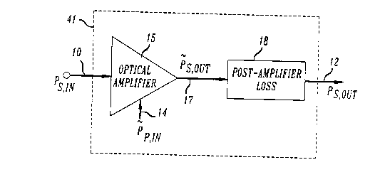
One embodiment realized in accordance with the principles of the invention
is shown in FIG. 4. In this embodiment, optical apl)a,atus 41 includes optical
5amplifier element 15 and post-amplifier loss element 18. Optical app~us 41 is
capable of being substituted for each optical amplifier 4 in FIG. 1. Optical amplifier
element 15 is pumped either co-directionally or contra-directionally or both co-directionally and contra-directionally via pump input 14 using pump input signalp ~, where p ~ is greater than Pp",. For the latter case of bidirectional
10pumping, two separate positions are required for pumping the amplifier element. The
source of the pump signal, although not shown in FIG. 4, is a light source such as
a laser having a sufficient output optical power at the a~p,ol fiate wavelength for
pumping optical amplifier 15. For erbium doped optical fiber amplifiers, suitable
pump wavelengths occur in the vicinity of 980nm and in the range of wavelengths
15from 1460nm to 1480nm for amplifying lightwave signals prop~g~ting at
approximately 1500nm. Of course, the aforementioned wavelengths are merely
illustrative and are not to be interpreted for purposes of limit~tion
Optical amplifier element 15 is optically coupled to post-amplifier loss
element 18 via fiber, waveguide, lens, or other optical coupling element on optical
20path 17. The output from optical amplifier 15 is output signal p which is a
larger output signal power than the design criterion P~ o~l- In order to compensate the
additional output signal power, post-amplifier loss element 18 provides an optical loss
L such that the total gain for the optical apparatus 41 is the product of the optical
loss of element 18 and the gain of optical amplifier 15. As a result, optical
25apparatus 41 exhibits an overall gain which is substantially identical to the gain for
the amplifier in FIG. 2 because the gain for either embodiment is PsoulPs~
Post-amplifier loss element 18 is realizable as any one of a variety of passive
and even active optical elements. For example, a fiber-to-fiber coupler having an
intentional misalignment between the two fibers to cause the desired amount of loss,
-8- 20828~9
L, is one contemplated implementation for loss element 18. Curvature or bending
of an optical fiber or dielectric waveguide subjects the lightwave signal to
controllable amounts of loss as a function of the radius for the curve or bend which
loss is sufficient to realize the post-amplifier loss element. Lightwave attenuation
S devices which include leaky or weakly guiding optical fibers and dielectric
waveguides provide another class of loss elemlont Passive and active (electrically
controllable) directional optical couplers provide a f~ed or adjustable amount of loss
to the lightwave signal on the straight-through waveguide path by coupling a portion
of the signal to the adja~,ent cross-over waveguide path. Variable amplitude optical
10 mo~ tors are also useful for alle~ ;ng the output signal from the optical amplifier
element by the desired loss amount, L. All devices described above for re~li7ing the
post-amplifier loss çlement have been disclosed in the technical lile,alulc and are
known to persons skilled in the art.
Post-amplifier loss element 18 is preferably realized as a passive loss element
15 having no nonline~r distortion. In ~d~lition~ it is desirable for loss element 18 to
inhibit or effectively reduce reflections back toward optical amplifier element 15.
Anti-reflective coatings and the like are suitable for minimi7ing and substantially
elimin~ting such reflections. ~ltern~tively, an optical isolator inserted between the
optical amplifier element and the post-amplifier loss element also minimi7P,s and even
20 elimin~t~,s the reflections toward optical amplifier çlçf,nt 15. This embodiment is
shown in FM. 5 wherein optical isolator 19 is inserted before loss element 18 toprovide a substantially unidirectional optical propagation from optical amplifier
element 15 to loss elemto,nt 18. Optical isolators of this type are collllll~,rcially
available and will not be described in further detail.
FIG. 6 shows an ~ltern~tive embodiment for optical amplifier element 15.
Optical amplifier element 15 is shown to include optical couplers 61 and 63 and an
amplifying fiber comprising doped optical fiber 62 and doped optical fiber 64. The
pump signal is coupled into optical amplifier element 15 via waveguide or fiber 16;
the optical input signal is coupled into optical amplifier element 15 via waveguide
or fiber 10. Output from optical amplifier element 15 is provided via waveguide or
fiber 17.
-9- ~0828~9
Optical coupler 61 couples the pump signal, p , into the waveguide path
with Ps~ so that the gain medium in doped optical fiber 62 is sufficiently inverted
for amplifying the input signal. Optical coupler 63 permits the amplified input signal
to be extracted from the optical amplifier element after the input signal has traversed
5 a predett;lll~ined length of the doped amplifying fiber 62. The predetermined length
of doped amplifier fiber is shown in FIG. 6 as substantially length x. Optical
coupler 63 may be a tap or coupling device capable of operating in either a
broadband mode or a narrowband mode. It is preferable to use a narrowband,
wavelength selective coupler for coupler 63 in order to substantially elimin~te further
10 propagation of the pump signal into the output of optical amplifier element 15.
As shown in FIG. 6, the pump signal is applied to optical amplifier
element lS for co-directional pumping. Contra-directional pumping is accomplished
by placing an optical coupler similar to coupler 61 at the opposite end of dopedoptical fiber 62 near coupler 63.
lS Optical coupler 63 is coupled to the doped optical fiber substantially at
distance x measured from the input end of the doped fiber. This arrangement permits
the optical amplifier element to provide the same colllpression level C in response
to the higher pump power p ~ as the compression obtained from pumping the
longer doped fiber comprising fibers 62 and 64 of length z with pump power Pp",.
20 For the longer fiber of length z being pumped at a higher pump power p ~, the
compression is greater than the specified compression level C as a result of thehigher pump power. Compression is reduced while maintaining a higher pump power
by coupling the amplified input signal out of the doped amplifying fiber after adistance x which is less than the distance z. It is instructive to view coupler 63 as
25 a slidable tap which couples light out of the doped amplifying fiber comprising fibers
62 and 64 for a total length z of fiber. In practice, however, it is contemplated that
the compression parameter is equally well ~tt~inçcl by physically shortening the total
lO- 20828~9
length of the doped amplifying fiber from length z to length x. By m~int~ining the
specified colllp~ession level, it is then possible to meet the amplifier design
pa~ lelels concerning compression, amplifier gain, and output power.
An illustration of the differences between the prior art optical amplifier and
S the arrangement of the present invention is shown in FIG. 7. Characteristics of the
optical amplifier from FIG. 2 are plotted in curve 71 for gain and curve 73 for noise
figure with the respective O~lalillg points 72 and 74 related to the specified output
power Pso~,t. Characteristics of the optical amplifier element in FM. 4 are plotted in
curve 75 for gain and curve 77 for noise figure with the respective O~la~ g points
10 76 and 78 for the optical amplifier element related to the higher output power
p . Compression for the prior art amplifier and the optical amplifier element of
the inventive arrangement is fixed to the specified parameter C. By adding the post-
amplification loss element to the optical amplifier arrangement, the operating points
for the arrangement become point 72, which has the specified gain G, and point 79,
15 which has a lower noise figure at the specified output power Pso",. The translation
of the operating points in the present arrangement occurs because the post-
amplification loss L causes a drop in gain by a factor L together with an outputpower reduction of L. Thus, the gain operating point moves down and left, each by
a factor L, from point 76 to point 72 whereas the noise figure moves only left from
20 point 78 to point 79.
FIGs. 8- 11 depict design considerations for the amplifier arrangement of FIG.
4 with either co-propagating or counter-propagating pump signals and with eitherlong or short wavelength pump signals. FIG. 8 shows the variation of noise figure
as a function of compression and post-amplifier loss L using long wavelength pump
25 signals in the optical amplifier element. FIG. 9 shows the variation of noise figure
as a function of compression and post-amplifier loss L using short wavelength pump
signals in the optical amplifier element. FIG. 10 shows the variation of pump power
as a function of compression and the post-amplifier loss L. FIG. 11 shows the
variation of amplifier length as a function of compression and the post-amplifier loss
30 L. For all the FIGs. 8- 11, it is understood that the amplifier arrangement is specified
- - 11- 208284g
to a gain of 7dB with an output power Psout of -lOdBm which are common
pa-~lRtels for soliton transmission systems. Similar characteristic curves are
derivable for NRZ tr~ncmi~sion systems.
Operation of the optical amplifier element in colllpl~ssion reduces signal
5 power fluctu~tions in the system. Introduction of post-amplifier loss reduces signal
power fluctuations only by an insignifi~nt amount. Post-amplifier loss provides a
signific~nt impact on system robustness in the presence of system~tic deviations in
pump power, amplifier length, and inter-amplifier loss for a system having c~sc~(l~l
amplifiers as shown in FIG. 1. These deviations result from pump laser aging,
10 ~t~,llla~ic m~nnfacturing imperfections, and design errors. It has now been found
that the use of the amplifier in FIG. 4 in the system of FIG. 1 permits the overall
system to operate closer to the system designed power level than is possible with the
prior art optical amplifiers of FIG. 2.
Prior art optical amplifiers continue to be ~esign~A in ways which minimi7~
15 the loss in the amplifier. This design approach requires more stringent fabrication
and device tolerances. In contrast with the prior art, the present invention shows that
it is possible to introduce signific~nt loss and different operating conditions for
amplifier in ways which are contrary to the prior art teachings. The present invention
by virtue of the post-amplific~tion loss and different operating conditions exhibits an
20 improved noise perform~nce while allowing more relaxed fabrication and operating
requirements on the component elements of the invention.