Note: Descriptions are shown in the official language in which they were submitted.
''~ ~ ~ 2~~~~~~1a9
- 2 -
FIELD'OF THE INVENTION
The present invention generally.relates to inkjet and
other types of printers and, more particularly, to the
printhead portion of an ink cartridge used in such
printers.
BACKGROUND OF THE INVENTION
Thermal inkjet print cartridges operate by rapidly
heating a small volume of ink to cause the ink to vaporize
and be ejected through one of a plurality of orifices so
as to print a dot of ink on a recording medium, such as a
sheet of paper. Typically, the orifices are arranged in
one or more linear arrays in a nozzle member. The
properly sequenced ejection of ink from each orifice
causes characters or other images to be printed upon the
paper as the printhead is moved relative to the paper.
The paper is typically shifted each time the printhead has
moved across the paper. The thermal inkjet printer is
fast and quiet, as or~l.y the ink strikes the paper. These
printers produce high quality printing and can be made~~
both compact and affordable.
In one prior art design, the inkjet printhead
general~y includes: (1) ink channels to supply ink from an
ink reservoir to each vaporization chamber~proximate to an
orifice; (2) a metal orifice plate or nozzle member in
which the orifices are formed in the required pattern; and
L:~M~2000~P\OOi.8D0
~082~~)
- 3 -
HP 192189
(3) a silicon substrate containing a series of thin film
resistors, one resistor per vaporization chamber.
To print a single dot of ink, an electrical current
from an external power supply is passed through a selected
thin film resistor. The resistor is then heated, in turn
superheating a thin layer of the adjacent ink within a
vaporization chamber, causing explosive vaporization, and,
consequently, causing a droplet of ink to be ejected
through an associated orifice onto the paper.
One prior art print cartridge is disclosed in U.S.
Patent No. 4,500,895 to Buck et al., entitled "Disposable
Inkjet Head,~~ issued February 19, 1985 and assigned to the
present assignee.
The prior art inkjet print cartridges include a
number of drawbacks: (1) the metal orifice plate is
expensive, difficult to form, and subject to corrosion;
(2) the metal orifice plate is difficult to align with the
heaters on the substrate and is difficult to affix to the
substrate using conventional techniques; (3) the supply of
ink to the vaporization chambers is sometimes routed
through a center slot formed in the substrate itself,
causing added manufacturing complexity and cost and
increasing the size of the substrate; and (4) the ink seal
between the back of the substrate and a print cartridge
body is time-consuming to form.
SUMMARY OF THE INVENTION
The present invention is an improved inkjet printhead
structure and method for forming the printhead which
avoids all the above-mentioned drawbacks with prior art
inkjet printheads.
In a printhead according to the preferred embodiment
of the invention, a polymer tape (nozzle member) having
orifices formed therein and containing conductive traces
is provided with one or more windows exposing ends of the
z: ~,~zooowool .sno
CA 02082852 2000-04-06
-4-
conductive traces. A conventional, commercially available automatic inner
lead bonder may then be used to automatically align heater resistors on a
substrate with the orifices in the nozzle member. This alignment step also
inherently aligns the electrodes on the substrate with the exposed ends of the
traces. The inner lead bonder then bonds the traces to the associated
substrate
electrodes through the windows formed in the tape.
The use of a nozzle member incorporating conductive traces thus not
only reduces the material cost of the printhead but reduces the cost of
assembly of the printhead.
A demultiplexer on the substrate greatly reduces the number of
electrodes and traces needed to provide energization signals to the heater
resistors.
The supply of ink to the orifices flows around the sides of the substrate
and into vaporization chambers, thus obviating the need for an ink feed slot
in
the substrate.
Further, since the nozzle member, having orifices formed therein, is
larger than the substrate and the substrate is affixed to the back of the
tape, an
ink seal may be easily created directly between the back surface of the tape
2 0 and the print cartridge body.
According to another aspect of the present invention there is provided
an inkjet print: cartridge comprising:
a print; cartridge body including an ink reservoir; and
a printhead, said printhead comprising:
2 5 a nozzle member having a plurality of ink orifices formed therein;
a substrate containing a plurality of heating elements, said substrate
mounted on a back surface of said nozzle member, each heating element being
located proximate to an associated ink orifice, said back surface of said
nozzle
member extending over two or more edges of said substrate;
3 0 conductors affixed to said nozzle member and connected to electrodes
formed on said substrate for supplying energization signals to said heating
elements; and
CA 02082852 2000-04-06
- 4a-
a barrier layer between said nozzle member and said substrate, said
barrier layer including a fluid channel communicating with said ink reservoir
to allow ink to flow around side edges of said substrate and into vaporization
chambers formed in said barrier layer, each vaporization chamber being
associated with an ink orifice in said nozzle member.
According to yet another aspect of the present invention there is
provided an ink jet print cartridge comprising:
a print cartridge body including an ink reservoir; and
a printhead, said printhead comprising:
a nozzle member having a plurality of ink orifices formed therein;
a substrate containing a plurality of heating elements, said substrate
mounted on a back surface of said nozzle member, each heating element being
located proximate to an associated ink orifice, said back surface of said
nozzle
member extending over two or more outer edges of said substrate; and
conductors affixed to said nozzle member and connected to electrodes
formed on said substrate for supplying energization signals to said heating
elements, whE;rein said nozzle member is formed of a flexible polymer
material and :.aid orifices are formed in said polymer material by laser
ablation
2 0 in a step-and-repeat process.
According to still yet another aspect of the present invention there is
provided an ink jet print cartridge comprising:
a print: cartridge body including an ink reservoir; and
a printhead, said printhead comprising:
2 5 a nozzle member having a plurality of ink orifices formed therein;
a substrate containing a plurality of heating elements, said substrate
mounted on a back surface of said nozzle member, each heating element being
located proximate to an associated ink orifice, said back surface of said
nozzle
member extending over two or more outer edges of said substrate;
3 0 conductors affixed to said nozzle member and connected to electrodes
formed on said substrate for supplying energization signals to said heating
element; and
CA 02082852 2000-04-06
-4b-
a barrier layer between said nozzle member and said substrate, said
barrier layer including ink conduits communicating with said ink reservoir and
vaporization chambers, each vaporization chamber being associated with an
orifice in said nozzle member.
BRIEF DESCRIPTION OF THE DRAWINGS
The present invention can be further understood by reference to the
following description and attached drawings which illustrate the preferred
l0 embodiment.
Other features and advantages will be apparent from the following
detailed description of the preferred embodiment, taken in conjunction with
the accompanying drawings, which illustrate, by way of example, the
principles of the invention.
~~~~~w
- 5 -
nr iyuey
Fig. 1 is a perspective view of an inkjet print
cartridge according to one embodiment of the present
invention.
Fig. 2 is a perspective view of the front surface of
the Tape Automated Bonding (TAB) printhead assembly
(hereinafter "TAB head assembly") removed from the print
cartridge of Fig. 1.
Fig. 3 is a perspective view of the back surface of
the TAB head assembly of Fig. 2 with a silicon substrate
mounted thereon and the conductive leads attached to the
substrate.
Fig. 4 is a side elevational view in cross-section
taken along line A-A in Fig. 3 illustrating the attachment
of conductive leads to electrodes on the silicon
substrate.
Fig. 5 is a perspective view of a portion of the
inkjet print cartridge of Fig. 1 with the TAB head
assembly removed.
Fig. 6 is a perspective view of a portion of the
inkjet print cartridge of Fig. 1 illustrating the
configuration of a seal which is formed between the ink
cartridge body and the TAB head assembly.
Fig. 7 is a top plan view, in perspective, of a
substrate structure containing heater resistors, ink
channels, and vaporization chambers, which is mounted on
the back of the TAB head assembly of Fig. 2.
Fig. 8 is a top plan view, in perspective, partially
cut away, of a portion of the TAB head assembly showing
the relationship of an orifice with respect to a
vaporization chamber, a heater resistor, and an edge of
the substrate.
Fig. 9 is a schematic cross-sectional view taken
along line B-B of Fig. 6 showing the seal between the TAB
head assembly and the print cartridge as well as the ink
flow path around the edges of the substrate.
L:\M\2000\P1001.BD0
2t~~~~~
_- - 6 -
Fig. 10 illustrates one process which may be used to
form the preferred TAB head assembly.
DETAILED DESCRIPTION OF THE PREFERRED EMBODIMENTS
Referring to Fig. 1, reference numeral 10 generally
indicates an inkjet print cartridge incorporating a
printhead according to one embodiment of the present
invention. The inkjet print cartridge 10 includes an ink
reservoir 12 and a printhead 14, where the printhead 14 is
formed using Tape Automated Bonding (TAB). The printhead
14 (hereinafter "TAB head assembly 14") includes a nozzle
member 16 comprising two parallel columns of offset holes
or orifices 17 formed in a flexible polymer tape 18 by,~
for example, laser ablation. The tape 18 may be purchased
commercially as Kapton"' tape, available from 3M
Corporation. Other suitable tape may be formed of Upilexn
or its equivalent.
A back surface of the tape 18 includes conductive
traces 36 (shown in Fig. 3) formed thereon using a
conventional photolithographic etching and/or plating
process. These conductive traces are terminated by large
contact pads 20 designed to interconnect with a printer.
The print cartridge 10 is designed to be installed in a
printer so that the contact pads 20, on the front surface
of the tape 18, contact printer electrodes providing
externally generated energization signals to the
printhead.
In the various embodiments shown, the traces are
formed on the back surface of the tape 18 (opposite the
surface which faces the recording medium). To access
these traces from the front surface of the tape 18, holes
(vias) must be formed through the front surface of the
tape 18 to expose the ends of the traces. The exposed
ends of the traces are then plated with, for example, gold
L:\IN\20001P\001.BD0
~ 192189
- 7 -
to form the contact pads 20 shown on the front surface of
the tape 18.
Windows 22 and 24 extend through the tape 18 and are
used to facilitate bonding of the other ends of the
conductive traces to electrodes on a silicon substrate
containing heater resistors. The windows 22 and 24 are
filled with an encapsulant to protect any underlying
portion of the traces and substrate.
In the print cartridge 10 of Fig. 1, the tape 18 is
bent over the back edge of the print cartridge "snout" and
extends approximately one half the length of the back wall
25 of the snout. This flap portion of the tape 18 is
needed for the routing of conductive traces which are
connected to the substrate electrodes through the far end
window 22.
Fig. 2 shows a front view of the TAB head assembly 14
of Fig. 1 removed from the print cartridge l0 and prior to
windows 22 and 24 in the TAB head assembly 14 being filled
with an encapsulant.
Affixed to the back of the TAB head assembly 14 is a
silicon substrate 28 (shown in Fig. 3) containing a
plurality of individually energizable thin film resistors.
Each resistor is located generally behind a single orifice
17 and acts as an ohmic heater when selectively energized
by one or more pulses applied sequentially or
simultaneously to one or more of the contact pads 20.
The orifices 17 and conductive traces may be of any
size, number, and pattern, and the various figures are
designed to simply and clearly show the features of the
invention. The relative dimensions of the various
features have been greatly adjusted for the sake of
clarity.
The orifice pattern on the tape 18 shown in Fig. 2
may be farmed by a masking process in combination with a
laser or other etching means in a step-and-repeat process,
L: \Ivn2000\P\OOI .BDO
r~
~~o~~~~
_ _s_
which would be readily understood by one of ordinary
skilled in the art after reading this disclosure.
Fig. 10, to be described in detail later, provides
additional detail of this process.
Fig. 3 shows a back surface of the TAB head assembly
14 of Fig. 2 showing the silicon die or substrate 28
mounted to the back of the tape 18 and also showing one
edge of a barrier layer 30 formed on the substrate 28
containing ink channels and vaporization chambers. Fig. 7
shows greater detail of this barrier layer 30 and will be
discussed later. Shown along the edge of the barrier
layer 30 are the entrances of the ink channels 32 which
receive ink from the ink reservoir 12 (Fig. 1).
The conductive traces 36 formed on the back of the
tape 18 are also shown in Fig. 3, where the traces 36
terminate in contact pads 20 (Fig. 2) on the opposite side
of the tape 18.
The windows 22 and 24 allow access to the ends of the
traces 36 and the substrate electrodes from the other side
of the tape 18 to facilitate bonding.
Fig. 4 shows a side view cross-section taken along
line A-A in Fig. 3 illustrating the connection of the ends
of the conductive traces 36 to the electrodes 40 formed on
the substrate 28. As seen in Fig. 4, a portion 42 of the
barrier layer 30 is used to insulate the ends of the
conductive traces 36 from the substrate 28.
Also shown in Fig. 4 is a side view of the tape 18,
the barrier layer 30, the windows 22 and 24, and the
entrances of the various ink channels 32. Droplets 46 of
ink are shown being ejected from orifice holes associated
with each of the ink channels 32.
Fig. 5 shows the print cartridge 10 of Fig. 1 with
the TAB head assembly 14 removed to reveal the headland
pattern 50 used in providing a seal between the TAB head
assembly 14 and the printhead body. The headland
L:\M\2000\P\OO1.BD0
1~ 192189
_ g _
characteristics are exaggerated for clarity. Also shown
in Fig. 5 is a central slot 52 in the print cartridge 10
for allowing ink from the ink reservoir 12 to flow to the
back surface of the TAB head assembly 14.
The headland pattern 50 formed on the print cartridge
is configured so that a bead of epoxy adhesive
dispensed on the inner raised walls 54 and across the wall
openings 55 and 56 (so as to circumscribe the substrate
when the TAB head assembly 14 is in place) will form an
10 ink seal between the body of the print cartridge 10 and
the back of the TAB head assembly 14 when the TAB head
assembly 14 is pressed into place against the headland
pattern 50. Other adhesives which may be used include
hot-melt, silicone, W curable adhesive, and mixtures
thereof. Further, a patterned adhesive film may be
positioned on the headland, as opposed to dispensing a
bead of adhesive.
When the TAB head assembly 14 of Fig. 3 is properly
positioned and pressed down on the headland pattern 50 in
Fig. 5 after the adhesive is dispensed, the two short ends
of the substrate 28 will be supported by the surface
portions 57 and 58 within the wall openings 55 and 56.
The configuration of the headland pattern 50 is such that,
when the substrate 28 is supported by the surface portions
57 and 58, the back surface of the tape 18 will be
slightly above the top of the raised walls 54 and
approximately flush with the flat top surface 59 of the
print cartridge 10. As the TAB head assembly 14 is
pressed down onto the headland 50, the adhesive is
squished down. From the top of the inner raised walls 54,
the adhesive overspills into the gutter between the inner
raised walls 54 and the outer raised wall 60 and
overspills somewhat toward the slot 52. From the wall
openings 55 and 56, the adhesive squishes inwardly in the
direction of slot 52 and squishes outwardly toward the
L:1M12000~P~001.BDO
~ tr ~ w
- 10 -
HP 192189
outer raised wall 60, which blocks further outward
displacement of the adhesive. The outward displacement of
the adhesive not only serves as an ink seal, but
encapsulates the conductive traces in the vicinity of the
headland 50 from underneath to protect the traces from
ink.
This seal formed by the adhesive circumscribing the
substrate 28 will allow ink to flow from slot 52 and
around the sides of the substrate to the vaporization
chambers formed in the barrier layer 30, but will prevent
ink from seeping out from under the TAB head assembly 14.
Thus, this adhesive seal provides a strong mechanical
coupling of the TAB head assembly 14 to the print
cartridge 10, provides a fluidic seal, and provides trace
encapsulation. The adhesive seal is also easier to cure
than prior art seals, and it is much easier to detect
leaks between the print cartridge body and the printhead,
since the sealant line is readily observable.
The edge feed feature, where ink flows around the
sides of the substrate and directly into ink channels, has
a number of advantages over prior art printhead designs
which form an elongated hole or slot running lengthwise in
the substrate to allow ink to flow into a central manifold
and ultimately to the entrances of ink channels. One
advantage is that the substrate can be made smaller, since
a slot is not required in the substrate. Not only can the
substrate be made narrower due to the absence of any
elongated central hole in the substrate, but the length of
the substrate can be shortened due to the substrate
structure now being less prone to cracking or breaking
without the central hole. This shortening of the
substrate enables a shorter headland 50 in Fig. 5 and,
hence, a shorter print cartridge snout. This is important
when the print cartridge is installed in a printer which
uses one or more pinch rollers below the snout's transport
L:1M\2000\P\001.BDO
" HP 192189
_ 11 _
path across the paper to press the paper against the
rotatable platen and which also uses one or more rollers
(also called star wheels) above the transport path to
maintain the paper contact around the platen. With a
shorter print cartridge snout, the star wheels can be
located closer to the pinch rollers to ensure better
paper/roller contact along the transport path of the print
cartridge snout.
Additionally, by making the substrate smaller, more
substrates can be formed per wafer, thus lowering the
material cost per substrate.
Other advantages of the edge feed feature are that.
manufacturing time is saved by not having to etch a slot
in the substrate, and the substrate is less prone to
breakage during handling. Further, the substrate is able
to dissipate more heat, since the ink flowing across the
back of the substrate and around the edges of the
substrate acts to draw heat away from the back of the
substrate.
There are also a number of performance advantages to
the edge feed design. Be eliminating the manifold as well
as the slot in the substrate, the ink is able to flow more
rapidly into the vaporization chambers, since there is
less restriction on the ink flow. This more rapid ink
flow improves the frequency response of the printhead,
allowing higher printing rates from a given number of
orifices. Further, the more rapid ink flow reduces
crosstalk between nearby vaporization chambers caused by
variations in ink flow as the heater elements in the
vaporization chambers are fired.
Fig. 6 shows a portion of the completed print
cartridge 10 illustrating, by cross-hatching, the location
of the underlying adhesive which forms the seal between
the TAB head assembly 14 and the body of the print
cartridge 10. In Fig. 6 the adhesive is located generally
L:1M120001P~001.BDO
- 12 -
HP 192189
between the dashed lines surrounding the array of orifices
17, where the outer dashed line 62 is slightly within the
boundaries of the outer raised wall 60 in Fig. 5, and the
inner dashed line 64 is slightly within the boundaries of
the inner raised walls 54 in Fig. 5. The adhesive is also
shown being squished through the wall openings 55 and 56
(Fig. 5) to encapsulate the traces leading to electrodes
on the substrate.
A cross-section of this seal taken along line B-B in
Fig. 6 is also shown in Fig. 9, to be discussed later.
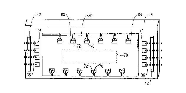
Fig. 7 is a front perspective view of the silicon
substrate 28 which is affixed to the back of the tape 18
in Fig. 2 to forth the TAB head assembly 14.
Silicon substrate 28 has formed on it, using
conventional photolithographic techniques, two rows of
offset thin film resistors 70, shown in Fig. 7 exposed
through the vaporization chambers 72 formed in the barrier
layer 30.
In one embodiment, the substrate 28 is approximately
one-half inch long and contains 300 heater resistors 70,
thus enabling a resolution of 600 dots per inch.
Also formed on the substrate 28 are electrodes 74 for
connection to the conductive traces 36 (shown by dashed
lines) formed on the back of the tape 18 in Fig. 2.
A demultiplexer 78, shown by a dashed outline in
Fig. 7, is also formed on the substrate 28 for
demultiplexing the incoming multiplexed signals applied to
the electrodes 74 and distributing the signals to the
various thin film resistors 70. The demultiplexer 78
enables the use of much fewer electrodes 74 than thin film
resistors 70. Having fewer electrodes allows all
connections to the substrate to be made from the short end
portions of the substrate, as shown in Fig. 4, so that
these connections will not interfere with the ink flow
around the long sides of the substrate. The demultiplexer
L:1M\2000\P\OO1.BDO
~ ~~i HP 192189
V
- 13 -
78 may be any decoder for decoding encoded signals applied
to the electrodes 74. The demultiplexer has input leads
(not shown for simplicity) connected to the electrodes 74
and has output leads (not shown) connected to the various
resistors 70.
Also formed on the surface of the substrate 28 using
conventional photolithographic techniques is the barrier
layer 30, which may be a layer of photoresist or some
other polymer, in which is formed the vaporization
chambers 72 and ink channels 80.
A portion 42 of the barrier layer 30 insulates the
conductive traces 36 from the underlying substrate 28, as
previously discussed with respect to Fig. 4.
In order to adhesively affix the top surface of the
barrier layer 30 to the back surface of the tape 18 shown
in Fig. 3, a thin adhesive layer 84, such as an uncured
layer of poly-isoprene photoresist, is applied to the top
surface of the barrier layer 30. A separate adhesive
layer may not be necessary if the top of the barrier layer
30 can be otherwise made adhesive. The resulting
substrate structure is then positioned with respect to the
back surface of the tape 18 so as to align the resistors
70 with the orifices formed in the tape 18. This
alignment step also inherently aligns the electrodes 74
with the ends of the conductive traces 36. The traces 36
are then bonded to the electrodes 74. This alignment and
bonding process is described in more detail later with
respect to Fig. 10. The aligned and bonded substrate/tape
structure is then heated while applying pressure to cure
the adhesive layer 84 and firmly affix the substrate
structure to the back surface of the tape 18.
Fig. 8 is an enlarged view of a single vaporization
chamber 72, thin film resistor 70, and frustum shaped
orifice 17 after the substrate structure of Fig. 7 is
secured to the back of the tape 18 via the thin adhesive
L:1M\2000\P\001.BDO
HP 192189
- 14 -
layer 84. A side edge of the substrate 28 is shown as
edge 86. In operation, ink flows from the ink reservoir
12 in Fig. 1, around the side edge 86 of the substrate 28,
and into the ink channel 80 and associated vaporization
chamber 72, as shown by the arrow 88. Upon energization
of the thin film resistor 70, a thin layer of the adjacent
ink is superheated, causing explosive vaporization and,
consequently, causing a droplet of ink to be ejected
through the orifice 17. The vaporization chamber 72 is
then refilled by capillary action.
In a preferred embodiment, the barrier layer 30 is
approximately 1 mils thick, the substrate 28 is approxi-
mately 20 mils thick, and the tape 18 is approximately
2 mils thick.
Shown in Fig. 9 is a side elevational view cross-
section taken along line B-B in Fig. 6 showing a portion
of the adhesive seal 90 surrounding the substrate 28 and
showing the substrate 28 being adhesively secured to a
central portion of the tape 18 by the thin adhesive layer
84 on the top surface of the barrier layer 30 containing
the ink channels and vaporization chambers 92 and 94. A
portion of the plastic body of the printhead cartridge 10,
including raised walls 54 shown in Fig. 5, is also shown.
Thin film resistors 96 and 98 are shown within the
vaporization chambers 92 and 94, respectively.
Fig. 9 also illustrates how ink 99 from the ink
reservoir 12 flows through the central slot 52 formed in
the print cartridge 10 and flows around the edges of the
substrate 28 into the vaporization chambers 92 and 94.
When the resistors 96 and 98 are energized, the ink within
the vaporization chambers 92 and 94 are ejected, as
illustrated by the emitted drops of ink 101 and 102.
In another embodiment, the ink reservoir contains two
separate ink sources, each containing a different color of
ink. In this alternative embodiment, the central slot 52
L:~IN~2000~P~OO1.BD0
~Q~~
_ - 15 -
in Fig. 9 is bisected, as shown by the dashed line 103, so
that each side of the central slot 52 communicates with a
separate ink source. Therefore, the left linear array of
vaporization chambers can be made to eject one color of
ink, while the right linear array of vaporization chambers
can be made to eject a different color of ink. This
concept can even be used to create a four color printhead,
where a different ink reservoir feeds ink to ink channels
along each of the four sides of the substrate. Thus,
instead of the two-edge feed design discussed above, a
four-edge design would be used, preferably using a square
substrate for symmetry.
Fig. 10 illustrates one method far forming the
preferred embodiment of the TAB head assembly 14 in
Fig. 3.
The starting material is a KaptonT" or Upilex''"-type
polymer tape 104, although the tape 104 can be any
suitable polymer film which is acceptable for use in the
below-described procedure. Some such films may comprise
teflon, polyimide, polymethylmethacrylate, polycarbonate,
polyester, polyamide polyethylene-terephthalate or
mixtures thereof.
The tape 104 is typically provided in long strips on
a reel 105. Sprocket holes 106 along the sides of the
tape 104 are used to accurately and securely transport the
tape 104. Alternately, the sprocket holes 106 may be
omitted and the tape may be transported with other types
of f fixtures .
In the preferred embodiment, the tape 104 is already
provided with conductive copper traces 36, such as shown
in Fig. 3, formed thereon using conventional metal
deposition and photolithographic processes. The
particular pattern of conductive traces depends on the
manner in which it is desired to distribute electrical
L:\IN\2000\P\001.BD0
_ 16 _
signals to the electrodes formed on silicon dies, which
are subsequently mounted on the tape 104.
In the preferred process, the tape 104 is transported
to a laser processing chamber and laser-ablated in a
pattern defined by one or more masks 108 using laser
radiation 110, such as that generated by an Excimer laser
112 of the FZ, ArF, KrCl, KrF, or XeCl type. The masked
laser radiation is designated by arrows 114.
In a preferred embodiment, such masks 108 define all
of the ablated features for an extended area of the tape
104, for example encompassing multiple orifices in the
case of an orifice pattern mask 108, and multiple
vaporization chambers in the case of a vaporization .
chamber pattern mask 108. Alternatively, patterns such as
the orifice pattern, the vaporization chamber pattern, or
other patterns may be placed side by side on a common mask
substrate which is substantially larger than the laser
beam. Then such patterns may be moved sequentially into
the beam. The masking material used in such masks will
preferably be highly reflecting at the laser wavelength,
consisting of, for example, a multilayer dielectric or a
metal such as aluminum.
The orifice pattern defined by the one or more masks
108 may be that generally shown in Fig. 2. Multiple masks
108 may be used to form a stepped orifice taper as shown
in Fig. 8.
In one embodiment, a separate mask 108 defines the
pattern of windows 22 and 24 shown in Figs. 2 and 3;
however, in the preferred embodiment, the windows 22 and
24 are formed using conventional photolithographic methods
prior to the tape 104 being subjected to the processes
shown in Fig. 10.
In an alternative embodiment of a nozzle member,
where the nozzle member also includes vaporization
chambers, one or more masks 108 would be used to form the
L:lIvn2000~P~001.BDO
FIP 192189
- 17 -
orifices and another mask 108 and laser energy level
(and/or number of laser shots) would be used to define the
vaporization chambers, ink channels, and manifolds which
are formed through a portion of the thickness of the tape
104.
The laser system for this process generally includes
beam delivery optics, alignment optics, a high precision
and high speed mask shuttle system, and a processing
chamber including a mechanism for handling and positioning
the tape 104. In the preferred embodiment, the laser
system uses a projection mask configuration wherein a
precision lens 115 interposed between the mask 108 and the
tape 104 projects the Excimer laser light onto the tape
104 in the image of the pattern defined on the mask 108.
The masked laser radiation exiting from lens 115 is
represented by arrows 116.
Such a projection mask configuration is advantageous
for high precision orifice dimensions, because the mask is
physically remote from the nozzle member. Soot is
naturally formed and ejected in the ablation process,
traveling distances of about one centimeter from the
nozzle member being ablated. If the mask were in contact
with the nozzle member, or in proximity to it, soot
buildup on the mask would tend to distort ablated features
and reduce their dimensional accuracy. In the preferred
embodiment, the projection lens is more than two
centimeters from the nozzle member being ablated, thereby
avoiding the buildup of any soot on it or on the mask.
Ablation is well known to produce features with
tapered walls, tapered so that the diameter of an orifice
is larger at the surface onto which the laser is incident,
and smaller at the exit surface. The taper angle varies
significantly with variations in the optical energy
density incident on the nozzle member for energy densities
less than about two joules per square centimeter. If the
L:\M\2000\P\OOi .BDO
_HP 192189
- 18 -
energy density were uncontrolled, the orifices produced
would vary significantly in taper angle, resulting in
substantial variations in exit orifice diameter. Such
variations would produce deleterious variations in ejected
ink drop volume and velocity, reducing print quality. In
the preferred embodiment, the optical energy of the
ablating laser beam is precisely monitored and controlled
to achieve a consistent taper angle, and thereby a
reproducible exit diameter. In addition to the print
quality benefits resulting from the constant orifice exit
diameter, a taper is beneficial to the operation of the
orifices, since the taper acts to increase the discharge
speed and provide a more focused ejection of ink, as well
as provide other advantages. The taper may be in the
range of 5 to 15 degrees relative to the axis of the
orifice. The preferred embodiment process described
herein allows rapid and precise fabrication without a need
to rock the laser beam relative to the nozzle member. It
produces accurate exit diameters even though the laser
2o beam is incident on the entrance surface rather than the
exit surface of the nozzle member.
After the step of laser-ablation, the polymer tape
104 is stepped, and the process is repeated. This is
referred to as a step-and-repeat process. The total
processing time required for forming a single pattern on
the tape 104 may be on the order of a few seconds. As
mentioned above, a single mask pattern may encompass an
extended group of ablated features to reduce the
processing time per nozzle member.
Laser ablation processes have distinct advantages
over other forms of laser drilling for the formation of
precision orifices, vaporization chambers, and ink
channels. In laser ablation, short pulses of intense
ultraviolet light are absorbed in a thin surface layer of
material within about 1 micrometer or less of the surface.
L:VvI\2000~P~001.BDO
CA 02082852 2000-04-06
-19-
Preferred pulse energies are greater than about 100 millijoules per square
centimeter and pulse durations are shorter than about 1 microsecond. Under
these conditions, the intense ultraviolet light photodissociates the chemical
bonds in the material. Furthermore, the absorbed ultraviolet energy is
concentrated in such a small volume of material that it rapidly heats the
dissociated fragments and ejects them away from the surface of the material.
Because these processes occur so quickly, there is not time for heat to
propagate to l:he surrounding material. As a result, the surrounding region is
l0 not melted or otherwise damaged, and the perimeter of ablated features can
replicate the shape of the incident optical beam with precision on the scale
of
about one micrometer. In addition, laser ablation can also form chambers with
substantially :flat bottom surfaces which form a plane recessed into the
layer,
provided the optical energy density is constant across the region being
ablated.
The depth of such chambers is determined by the number of laser shots, and
the power density of each.
Laser-ablation processes also have numerous advantages as compared
to conventional lithographic electroforming processes for forming nozzle
members for inkjet printheads. For example, laser-ablation processes
2 0 generally are less expensive and simpler than conventional lithographic
electroforming processes. In addition, by using laser-ablations processes,
polymer nozzle members can be fabricated in substantially larger sizes (i.e.,
having greater surface areas) and with nozzle geometries that are not
practical
with conventional electroforming processes. In particular, unique nozzle
2 5 shapes can be produced by controlling exposure intensity or making
multiple
exposures with a laser beam being reoriented between each exposure.
CA 02082852 2000-04-06
-20-
Also, precise nozzle geometxies can be formed without process
controls as strict as those required for electroforming processes.
Another advantage of forming nozzle members by laser-ablating a
polymer material is that the orifices or nozzles can be easily fabricated with
various ratios of nozzle length (L) to nozzle diameter (D). In the preferred
embodiment, the L/D ratio exceeds unity. One advantage of extending a
nozzle's length relative to its diameter is that orifice-resistor positioning
in a
vaporization chamber becomes less critcal.
1 o In use, laser-ablated polymer nozzle members for inkjet printers have
characteristics that are superior to conventional electroformed orifice
plates.
For example, laser-ablated polymer nozzle members are highly resistant to
corrosion by water-based printing inks and are generally hydrophobic.
Further, laser-ablated polymer nozzle members have a relatively low elastic
modulus, so built-in stress between the nozzle member and an underlying
substrate or barrier layer has less of a tendency to cause nozzle member-to-
barrier layer delamination. Still further, laser-ablated polymer nozzle
members can be readily fixed to, or formed with, a polymer substrate.
Although an Excimer laser is used in the preferred embodiments, other
2 0 ultraviolet light sources with substantially the same optical wavelength
and
energy density may be used to accomplish the ablation process. Preferably,
the wavelength of such an ultraviolet light source will lie in the 150 nm to
400 nm range to allow high absorption in the tape to be ablated. Furthermore,
- 21 - 2(~8~~~
the energy density should be greater than about 100
millijoules per square centimeter with a pulse length
shorter than about 1 microsecond to achieve rapid ejection
of ablated material with essentially no heating of the
surrounding remaining material.
As will be understood by those of ordinary skill in
the art, numerous other processes for forming a pattern on
the tape 104 may also be used. Other such processes
include chemical etching, stamping, reactive ion etching,
ion beam milling, and molding or casting on a photodefined
pattern.
A next step in the process is a cleaning step wherein
the laser ablated portion of the tape 104 is positioned,
under a cleaning station 117. At the cleaning station
117, debris from the laser ablation is removed according
to standard industry practice.
The tape 104 is then stepped to the next station,
which is an optical alignment station 118 incorporated in
a conventional automatic TAB bonder, such as an inner lead
bonder commercially available from Shinkawa Corporation,
model number IL-20. The bonder is preprogrammed with an
alignment (target) pattern on the nozzle member, created
in the same manner and/or step as used to created the
orifices, and a target pattern on the substrate, created
in the same manner and/or step used to create the
resistors. In the preferred embodiment, the nozzle member
material is semi-transparent so that the target pattern on
the substrate may be viewed through the nozzle member.
The bonder then automatically positions the silicon dies
120 with respect to the nozzle members so as to align the
two target patterns. Such an alignment feature exists in
the Shinkawa TAB bonder. This automatic alignment of the
nozzle member target pattern with the substrate target
pattern not only precisely aligns the orifices with the
resistors but also inherently aligns the electrodes on the
L:\M\2000\P\OO1.BDO
_ 22 _
dies 120 with the ends of the conductive traces formed in
the tape 104, since the traces and the orifices are
aligned in the tape 104, and the substrate electrodes and
the heating resistors are aligned on the substrate.
Therefore, all patterns on the tape 104 and on the silicon
dies 120 will be aligned with respect to one another once
the two target patterns are aligned.
Thus, the alignment of the silicon dies 120 with
respect to the tape 104 is performed automatically using
l0 only commercially available equipment. By integrating the
conductive traces with the nozzle member, such an
alignment feature is possible. Such integration not only
reduces the assembly cost of the printhead but reduces the
printhead material cost as well.
The automatic TAB bonder then uses a gang bonding
method to press the ends of the conductive traces down
onto the associated substrate electrodes through the
windows formed in the tape 104. The bonder then applies
heat, such as by using thermocompression bonding, to weld
the ends of the traces to the associated electrodes. A
side view of one embodiment of the resulting structure is
shown in Fig. 4. Other types of bonding can also be used,
such as ultrasonic bonding, conductive epoxy, solder
paste, or other well-known means.
The tape 104 is then stepped to a heat and pressure
station 122. As previously discussed with respect to Fig.
7, an adhesive layer 84 exists on the top surface of the
barrier layer 30 formed on the silicon substrate. After
the above-described bonding step, the silicon dies 120 are
then pressed down against the tape 104, and heat is
applied to cure the adhesive layer 84 and physically bond
the dies 120 to the tape 104.
Thereafter the tape 104 steps and is optionally taken
up on the take-up reel 124. The tape 104 may then later
L:11H\2000~P~001.BDO
ru' w211sy
- 23 -
be cut to separate the individual TAB head assemblies from
one another.
The resulting TAB head assembly is then positioned on
the print cartridge 10, and the previously described
adhesive seal 90 in Fig. 9 is formed to firmly secure the
nozzle member to the print cartridge, provide an ink-proof
seal around the substrate between the nozzle member and
the ink reservoir, and encapsulate the traces in the
vicinity of the headland so as to isolate the traces from
the ink.
Peripheral points on the flexible TAB head assembly
are then secured to the plastic print cartridge 10 by a
conventional melt-through type bonding process to cause
the polymer tape 18 to remain relatively flush with the
surface of the print cartridge 10, as shown in Fig. 1.
The foregoing has described the principles, preferred
embodiments and modes of operation of the present
invention. However, the invention should not be construed
as being limited to the particular embodiments discussed.
As an example, the above-described inventions can be used
in conjunction with inkjet printers that are not of the
thermal type, as well as inkjet printers that are of the
thermal type. Thus, the above-described embodiments
should be regarded as illustrative rather than
restrictive, and it should be appreciated that variations
may be made in those embodiments by workers skilled in the
art without departing from the scope of the present
invention as defined by the following claims.
L: \M\2000\P1001. BDO