Note: Descriptions are shown in the official language in which they were submitted.
Optical Transmitter For An Optical Modulator
BACKGROUND OF THE INVENTION:
Field of the Invention:
The present invention relates to an optical
transmitter for use with an optlcal communlcatlon system and,
more partlcularly, to lmprovements of an optlcal transmltter
having an optical modulator.
Heretofore, optical transmitters used by optical
communication systems have adopted the so-called direct
modulatlon as their operating principle. The method involves
modulating the current that flows through laser diodes by use
of data signals. A ma~or drawback of direct modulation is
the difficulty in implementing long-distance data
transmission due to wavelength dispersion. Efforts of recent
years to circumvent the disadvantage have led to the
development of external modulation. This is the kind of
optical modulation that is hlghly lmmune to the adverse
effects of wavelength dlsperslon over optlcal flber cables.
For example, what ls known as the LlNbO3 Mach-Zehnder
modulator has drawn attentlon for lts excellent modulatlon
characterlstlc and hlgh resistance to wave-length disperslon.
Optlcal transmitters based on the external modulation
principle are sub~ect to a number of requirements: (a) the
operating point of the optlcal modu-
28170-50
~.
ZC~3~9
lator should be controlled to be stable; (b) the optical
modulator should be driven with a low voltage; (c) there
should be minimum waveform distortion attributable to the
capacitor between a driving circuit and the electrodes of
the optical modulator as well as to the capacitor between
the electrodes and a terminating resistor; and (d) there
should be minimum changes in modulation characteristic
which are attributable to abrupt changes in the so-called
mark rate. It is also required that the presence or
absence of chirping (dynamic wavelength fluctuation) in
the optical signal output by the optical modulator be
optional. For example, where long-distance transmission
is effected using a wavelength that approximately matches
the zero-dispersion wavelength of the optical fiber and
where the dispersion value can be either positive or nega-
tive, there should be no chirping. On the other hand,
where the polarity of the wavelength dispersion of the
optical fiber is predetermined and where optical pulse
compression may be effected using a kind of chirping that
corresponds to the dispersion polarity, the presence of
chirping should be selected.
Description of the Related Art:
The typical Mach-Zehnder modulator comprises an input
port that receives light from a light source, a pair of
branching t~aveguides that transmit the light received
through the input port after branchillg the light in t~o
directions, an OUtp-lt port that converges the branched
ligllt strenms coming O~lt of the brnnching ~~aveg-lides, and
5 cloclrodos tllnl; give ~ rlsc charlgc to tl~e li~ht trar~slllilted
through the branching l~aveguides. I~hen the light streams
from the branching waveguides converge in phase (with a
phase difference of 2 n~ , n being an integer), the light ~
output is turned on; ~~hen the light streams converge
opposite to each other in phase (with a phase difference
of (2n + 1)~ , n being an integer), the light OUtp~lt is
turned off. Thus intensity modulation is performed by
varying the voltage given to the electrodes by use of an
input signal. Where the voltage fed to the electrodes is
varied as per the input signal, it is necessary to compen-
sate for the operating point drift of the optical modula-
tor caused by temperature fluctuation and other ambient
conditions. One ~ay to do this is first to supply the
electrodes ~ith a bias voltage such as to keep the operat-
ing point ~here optimum and then to superimpose asignnl onto the bias voltage so that the output light is
turned on and off ~hile the operating point is being held
in its optimum position. Prior art techniques of the
above l;ind for stabilizing the operating point of the
optical modulator ar~ described illustratively in Japanese
3 --
28170-50
Patent Laid-Open No. 49-42365 and in Japanese Patent Laid-
Open No. 3-251815.
Also known is a Mach-Zehn~er optical modulator of a
symmetrical dual electrode driving type designed to lower the
voltage to a signal electrode of the optical modulator and to
eliminate chirping in the modulated output light. That is,
the branching waveguides have a signal electrode each. These
electrodes are fed with driving voltages opposite to each
other in phase. This technique is disclosed illustratively
in Technical Digest of IOOC' 89, l9D4-2, 1989, "Perfectly
Chirpless Low Drive Voltage Ti:LiNbO3 Mach-Z~hn~er Modulator
with Two Traveling-Wave Electrodes".
There has also been disclosed related techniques of
the optical transmitter permitting the selection of the
presence or absence of chirping.
The driving signal for optical modulation has a
repetitive pulse waveform or an AC waveform, while the bias
voltage for operating point control comes from a DC source.
Thus the circuit for controlling the operating point is
connected to the electrode in a DC setup, whereas the driving
circuit is connected to the electrode in an AC setup via a
capacitor for DC decoupling. Where the electrode of the
optical modulator is built as a traveling-wave type, the
electrode is connected to the terminating
-- 4
28170-50
reslstor also ln an AC setup. If there exists a capacltor
between the drlvlng clrcult and the electrode and/or between
the termlnatlng reslstor and the electrode, the low-frequency
component of the drlvlng slgnal ls cut off. Thls can promote
dlstortlon of the slgnal waveform of the modulatled light
upon abrupt change ln the mark rate. If the frequency
characterlstlc of the capacltor ls lnsufflclent, the waveform
of the drlvlng slgnal of as hlgh as several Gb/s ls dlstorted
by the capacltor. That ln turn dlstorts the waveform of the
modulated llght.
Whereas the symmetrlcal dual electrode type optlcal
modulator may lower the drlvlng voltage, lts appllcatlon to
the optlcal transmltter wlth a stablllzed operatlng polnt ls
yet to be lmplemented extenslvely.
SUMMARY OF THR INV~NTION:
It ls therefore an ob~ect of the present lnventlon
to provlde an optlcal modulator that has stable control on
the operatlng polnt and has llttle waveform dlstortlon
agalnst the change ln the mark rate by ellmlnatlng the
capacitor connectlng the electrode of the optlcal modulator
to the drlvlng clrcult.
It ls another ob~ect of the lnventlon to provlde an
optlcal transmltter that ellmlnates the capacltor connectlng
the electrode to the termlnatlng reslstor lf the electrode ls
bullt as a travellng-wave type.
It ls a further ob~ect of the lnventlon to provlde
an optlcal modulator that lowers the drlvlng voltage thereof.
,~ 28170-50
, ,,J
It ls yet another object of the invention to
provide an optical modulator that permits easy selection of
the presence or absence of chirping in the optical signal
output thereof.
In carrylng out the invention and according to one
aspect thereof, there is provided an optical modulator
comprising: a light source; a Mach-Zehnder optical modulator
having an input port which receives light from the light
source, a first and a second branching waveguide which
transmit the light supplied to the input port after branching
the supplied light in two directions, an output port which
converges the branched light from the first branching
waveguide and the second branching waveguide before
outputting the converged light, and a signal electrode and a
bias electrode which are insulated from each other and which
give phase change to the light transmltted through the first
branching waveguide and the second branching waveguide; light
branching means, connected operatively to the output port,
for branching in two directions the light output by the
output port; driving
- ~ 28170-50
means, connected operatively to the signal electrode, for
s~lpplying the signal electrode ~~ith a driving signal based
on an inp~lt signal; and operatinS l~oint control means,
connected operatively t,o the bias electrode, for sul>l)lying
5 the bias electrode ~~ith ~ bias volt-age controlled in
accordance ~iith the ligllt branched by the light branching
means for control of the operating point of the Mach-
Zehnder optical mod~llator.
According to another aspect of the invention, there
is provicled an optical modulator comprising: a light
so~lrce; a ~lach-Zehnder optical mod~llator, connected opera-
tively to the light so~lrce, for modulating in intensity
the light from the light source; and driving means, con-
nected operatively to the Mach-Zehnder optical modulcltor,
for supplying the optical mod~llator ~~ith a driving signal
based on an inp~lt signal; the Mach-Zehnder optical mod~lla-
tor including: an inp~lt-side optical ~~aveguide; a first
branching portion for branching in two directions the
light transmitt,ed through the input-side optical wave-
~lide; a first and a second branching ~aveguide for tralls-
mitting the light branched by the first branching portion;
a second branching portion for converging the light trans-
mitted through the first branching ~~aveguide and the
sccol-ld brancllirlO waveguide; an output-side optical wave-
g~lide for transmitting the light converged by the second
~8170-5
~;~
branchlng portion; a first and a second loaded electrode
loaded respectively onto the first branching wavegulde and
the second branching wavegulde; a delay optlcal wavegulde
coupled directlonally to at least one of the first branching
waveguide and the second branchlng waveguide; and a control
electrode for controlllng the coupllng ratlo of the
dlrectlonal coupllng between the branchlng wavegulde and the
delay optlcal wavegulde.
In accordance with the present lnventlon there ls
provlded an optlcal modulator comprlslng: an optlcal
lnterferometer type modulatlng means havlng an lnput port
whlch recelves light from a llght source, a flrst and a
second branchlng wavegulde whlch transmlt the llght supplled
to sald lnput port after branchlng the supplled llght ln two
dlrectlons, an output port whlch converges the branched llght
from sald first branchlng waveguide and sald second branchlng
wavegulde before outputtlng the converged llght, and a slgnal
electrode and a blas electrode whlch are lnsulated from each
other and whlch give a phase change to the llght transmltted
through sald flrst branchlng wavegulde and sald second
branchlng wavegulde; drlvlng means directly connected to said
slgnal electrode ln a DC setup, for supplylng sald slgnal
electrode with a driving slgnal based on an lnput slgnal; and
operatlng point control means operatively connected to sald
blas electrode, for supplylng sald blas electrode wlth a blas
voltage controlled ln accordance wlth the llght output from
sald output port for control of the operatlng polnt of sald
modulatlng means.
-- 8
28170-50
;' ~
In accordance wlth the present lnventlon there ls
also provlded an optical modulator comprlslng an optlcal
interferometer type modulatlng means for modulatlng lntensity
llght from a llght source; and drlvlng means, connected
operatlvely to sald modulating means for supplylng sald
modulatlng means wlth a drlvlng slgnal based on an lnput
slgnal; sald modulatlng means lncludlng: an lnput-slde
optlcal wavegulde; a flrst branchlng portlon for branchlng ln
two dlrectlons the llght transmltted through sald lnput-slde
optical waveguide; a flrst and a second branchlng wavegulde
for transmlttlng the llght branched by sald flrst branchlng
portlon; a second branchlng portlon for converglng the llght
transmltted through sald flrst branchlng wavegulde and sald
second branchlng wavegulde; an output-slde optlcal wavegulde
for transmlttlng the llght converged by sald second branchlng
portlon; a flrst and second electrode cooperatlng
respectively wlth sald flrst branchlng wavegulde and sald
second branchlng wavegulde; a delay optlcal wavegulde coupled
dlrectlonally to at least one of sald flrst branchlng
wavegulde and sald second branchlng wavegulde; and a control
electrode for controlllng the coupllng ratlo of the
dlrectlonal coupllng between sald at least one branchlng
wavegulde and sald delay optlcal wavegulde.
The above and other ob~ects, features and
advantages of the present lnventlon and the manner of
reallzlng them wlll become more apparent, and the lnventlon
ltself wlll best be understood from a study of the followlng
descrlptlon and appended clalms wlth reference to the
- 8a -
28170-50
7 ~ ~
attached drawings showlng some preferred embodiments of the
lnventlon.
BR BF DK~L~ I ~110N OF THF DRAWINGS
Flg. 1 ls a plan vlew of a Mach-Zehnder optlcal
modulator that may be used to practlce the lnventlon;
Flg. 2 ls a cross-sectlonal vlew taken on llne A-A
of the optlcal modulator ln Flg. l;
Flg. 3 ls a cross-sectlonal vlew of another optlcal
modulator that may be used to practlce the lnventlon;
Flg. 4 ls a plan vlew of another optlcal modulator
that may be used to practlce the lnvention;
- 8b -
28170-50
_. ? ' - -
3~19
Fig. 5 is a view illustrating the input/output cha-
racteristic of a Mach-Zehnder optical modulator;
Fig. 6 is a block diagram of an optical transmitter
used to implement symmetrical modulation;
Fig. 7 is a set of views depicting the waveforms of
an optical signal output from the optical transmitter of
Fig. 6;
Figs. 8 and 9 are views illustrating the waveforms of
optical signal outputs effected by the optical transmitter
of Fig. 6 when the transmitter develops an operating point
drift in the positive and negative directions;
Fig. 10 is a view illustrating typical probabilities
of occurrence of the space portion, mark portion, and
leading and trailing portion of an eye pattern;
Fig. 11 is a block diagram of an optical transmitter
practiced as a first embodiment of the invention;
Figs. 12A through 12E are views of waveforms generat-
ed by the optical transmitter of Fig. 11 as it is operat-
ing;
Fig. 13 is a schematic view depicting key parts of an
optical transmitter practiced as a second embodiment of
the invention;
Fig. 14 is a block diagram of the entire optical
transmitter of Fig. 13;
Figs. I5A through 15G are views of waveforms generat-
~G! 3~9
ed by the optical transmitter of Fig. 14 as it is operat-
ing;
Fig. 16 is a block diagram of an optical transmitter
practiced as a third embodiment of the invention;
Figs. 17A through 17H are views of waveforms generat-
ed by the optical transmitter of Fig. 16 as it is operat-
ing ;
Fig. 18 is a block diagram of an optical transmitter
practiced as a fourth embodiment of the invention;
Figs. l9A through l9G are views of waveforms generat-
ed by the optical transmitter of Fig. 18 as it is operat-
ing;
Fig. 20 is a plan view of an optical modulator for
use with an optical transmitter practiced as a fifth
embodiment of the invention;
Fig. 21 is a cross-sectional view taken on line B-B
of the optical modulator of Fig. 20;
Figs. 22A and 22B are views showing how optical
coupling is accomplished at a directionally coupled part
in connection with the invention;
Fig. 23 is a view depicting how optical transmission
paths are switched in the optical modulator of Fig. 20;
Fig. 24 is a plan view of an optical modulator for
use with an optical transmitter practiced as a sixth
embodiment of the invention;
-- 10 --
J ~
Fig. 25 is a cross-sectional view tal;en on line C-C
of the optical mod~llator in Fig. 2~;
Fig. 26 is a plan view of an optical modulator for
use with an optical transmitter prncticed as a seventh
r) cml~o(li.mcnl; Or th(' invenl;ion;
Fig. 27 is a plan view of an optical modulator for
use with an optical transmitter practiced as an eighth
embodiment of the invention; and
Fig. 28 is a plan view of an optical modulator for
use with an optical transmitter practiced as ~t ninth
embodiment of the in~ention.
DESCnIPTION OF THE PREFERRED EMBODIMENT:
The preferred embodiments of the invention will now
be described in detail with reference to the accompanying
drawings.
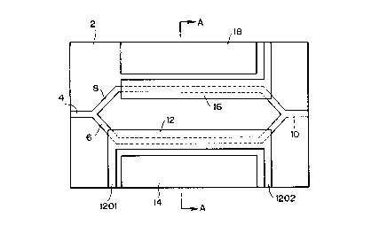
Fig. 1 is a plan view of a Mach-Zehnder optical
modulator that may be used to practice the invention, and
Fig. 2 is a cross-sectional view talcen on line A-A of that
ol~tical modulator. 'I'he optical modulator comprises a Z-
cut type LiNbO3 substrate into which titani~lm (Ti) is
thermnlly dispersed to form optical waveguides thereon.
The optical waveguides are loaded with electrodes. The
optical waveguides formed on the substrate 2 include an
inptlt port 4 that receives light from a light source, not
28170-50
:. -
'~C~3'~3L9
shown; a pair of branching waveguides 6 and 8 which trans-
mit the light from the input port 4 after branching the
received light in two directions; and an output port 10
that converges the branched light transmitted through the
branching waveguides 6 and 8. The branching waveguides 6
and 8 are loaded respectively with a signal electrode 12
and a bias electrode 16. Reference numeral 14 indicates a
grounding electrode located close to the signal electrode
12, while reference numeral 18 is a grounding electrode
furnished close to the bias electrode 16. Although a
buffer layer 20 composed primarily of SiO2 iS formed
between each electrode and the substrate 2, this layer is
omitted from ~ig. 1 so as to maintain the visibility of
other key components.
A driving signal is applied across the signal elec-
trode 12 to the grounding electrode 14, and a bias voltage
is fed between the bias electrode 16 and the grounding
electrode 18. The signal electrode 12 is built as a
traveling-wave type that allows the electric field of the
driving signal to travel in the same direction as that of
the light through the branching waveguide 6. The driving
signal is supplied from an upstream edge 1201 of the
signal electrode 12. A downstream edge 1202 of the signal
electrode 12 is provided with a terminating resistor, to
be described later. Built as a traveling-wave type, the
- 12 -
.9
signal electrode 12 permits appreciably higher mod~llation
than electrodes of other types. Because the substrate of
this example is a Z-cut type, the branching waveguides 6
and 8 are loaded from directly above with the signal
electrode 12 and bias electrode 16, respectively, with the
grounding electrodes 14 and 18 located close to the elec-
trodes 12 and 16, respectively. This arrangement permits
effective application of the electric field to the branch-
ing waveguides 6 and 8. Where the substrate is made of Z-
cut LiNbO3, the electric field is applied effectively tothe branching waveguides in the manner described below.
Fig. 3 is a cross-sectional view of another optical
modulator that may be used to practice the invention. In
this example, the branching waveguides 6 and 8 are loaded
from directly above with the signal electrodes 12 and 16,
respectively, and a common grounding electrode 22 is
formed on the back side of the substrate 2. Forming the
signal electrode, bias electrode and grounding electrode
on different planes as illustrated still affords necessary
phase change to the light transmitted through the branch-
ing waveguides.
Fig. 4 is a plan view of another optical modulator
that may be used to practice the invention. While the
typical optical modulators described so far have one of
the two branching waveguides loaded with the signal
- 13 -
3~9
electrode and the other loaded with the bias electrode,
this optical modulator has one of the branching waveguides
8 loaded with the signal electrode 12 and bias electrode
16 and has the other branching waveguide 6 furnished with
the grounding electrodes 14 and 18 corresponding respec-
tively to the signal electrode 12 and bias electrode 16.
Where the signal electrode is insulated from the bias
electrode as described, there may be various modes to
choose from in which to construct the signal and bias
electrodes. If optical waveguides are formed on a crystal
plane other than the Z-cut plane of LiNbO3, the electrode
layout may be varied so as to permit optimally effective
application of the electric field. For example, the
electrodes may be formed alongside of the branching wave-
guides.
The mutually isolated signal electrode and biaselectrode characterize the Mach-Zehnder optical modulator.
The advantages of this type of modulator are highlighted
illustratively by describing the operating characteristic
of an ordinary optical modulator in which the signal and
bias electrodes are integrally furnished. One such ordi-
nary optical modulator may be the one in Fig. 4 minus the
bias electrode 16 and grounding electrode 18.
Fig. 5 illustrates the input/output characteristic of
a typical Mach-Zehnder optical modulator. In Fig. 5,
- 14 -
2~3~9
reference numeral (1) indicates the characteristic in
effect before an operating point drift occurs, and refer-
ence numeral (2) points to the characteristic in effect
after an operating point drift has occurred. The operat-
ing point drift refers to a drift in the direction ofvoltage increase or decrease along the operation charac-
teristic curve indicating the relationship between output
light power and driving voltage. As depicted, the opera-
tion characteristic curve of the Mach-Zehnder optical
modulator has periodicity with respect to the voltage
change. Thus the use of driving voltages Vo and Vl for
which the output light power is both minimized and maxi-
mized permits efficient binary modulation. With the
optical signal output by that Mach-Zehnder optical modula-
tor, the driving voltages Vo and V1 staying constant uponoccurrence of an operating point drift cause waveform
distortion and extinction ratio deterioration due to the
above-mentioned periodicity. Where the operating point
drift is represented by dV, the drift should preferably be
compensated by calculations of Vo + dV and Vl + dV, where
Vo and V1 are the driving voltages. One known method for
controlling the operating point in compensation for its
drift is described illustratively in Japanese Patent Laid-
Open No. 49-42365. This method involves driving the
optical modulator by superimposing a low-frequency signal
- 15 -
26~53~9
onto one of the two logic levels of a driving signal. The
operating point is then controlled by use of the phase of
the low-frequency signal detected from the optical signal
output. However, in the case of asymmetrical modulation
involving the superimposing of the low-frequency signal
onto one of the two logic levels of the driving signal
(here, "modulation" refers not to the modulation for
signal transmission but to the modulation based on a low-
frequency signal for operating point control), the optimum
operating point may not be maintained if the rise time or
fall time of the input signal is significantly long (the
reason for this will be discussed later in quantitative
terms). As disclosed in Japanese Patent Laid-Open No. 3-
251815, there is a prior art method of symmetrical modula-
tion for operating point control whereby waveform distor-
tion of the output optical signal and e~tinction ratio
deterioration following the operating point drift are
prevented without regard to the input signal. How the
symmetrical modulation method is practiced and how it
works will be described below in detailed quantitative
terms because a study of this method is deemed indispens-
able for better understanding the advantages of the
present invention.
Fig. 6 is a block diagram of an optical transmitter
used to implement symmetrical modulation. In Fig. 6, a
- 16 -
3~9
Mach-Zehnder optical modulator 26 having a signal elec-
trode 12 is supplied with light from a light source 24.
The output light from the optical modulator 26 is branched
in two directions by an optical branching circuit 28. One
of the two light streams branched by the optical branching
circuit 28 is used as an optical signal output, and the
other light stream is converted to an electrical signal by
an optical-to-electrical signal converter 30. A low-fre-
quency superimposing circuit 36 superimposes a low-fre-
quency signal from an oscillator 34 onto a driving signalfrom a driving circuit 32. After the superimposing of the
low-frequency signal, the driving signal is fed to the
signal electrode 12 via a capacitor C of a bias tee 38.
The output terminal of the signal electrode 12 is connect-
ed via a capacitor C of a bias tee 40 illustratively to a50-ohm terminating resistor 42. A phase detecting circuit
44 compares in phase the frequency component of the low-
frequency signal in the electrical signal from the opti-
cal-to-electrical signal converter 30 with the low-fre-
quency signal rrom the oscillator 34. The phase detectingcircuit 44 then outputs a DC signal whose polarity is
determined by the direction of the operating point drift
and whose level depends on the magnitude of the drift. A
bias control circuit 46 provides feedback control on the
bias voltage to the signal electrode 12 in such a way that
- 17 -
2C~19
the DC signal coming from the phase detecting circuit 44
becomes zero.
As indicated by (a) in Fig. 7, the waveform of the
driving signal to be converted to an optical signal by the
Mach-Zehnder optical modulator 26 shows that low-frequency
signals are superimposed opposite to each other in phase
on the space side and the mark side of the driving signal
(i.e., symmetrical modulation). When this driving signal
drives the optical modulator 26 having input/output char-
acteristic (operation characteristic curve) indicated by(b) in Fig. 7, the optical modulator 26 yields an output
optical signal. As illustrated by (c) in Fig. 7, this
output optical signal is a signal that is amplitude-modu-
lated with a signal having a frequency of 2 fo (fo is the
frequency of the low-frequency signal). Where there is no
operating point drift, the driving voltages Vo and V1
matching the two logic levels of the input signal corre-
spond to the minimum and maximum values located adjacent
to one another along the operation characteristic curve.
Thus in the output optical signal, the envelope on the
space side becomes opposite in phase to the envelope on
the mark side, and the frequency of the superimposed
component is 2 fo. It follows that the frequency compo-
nent of fo is not detected from the output of the optical-
to-electrical signal converter 30. But if an operating
- 18 -
point drift occurs, the space-side envelope and the mark-
side envelope in the OlltpUt optical signal become in phase
~~ith each other, as depicted in ~igs. 8 and 9. The mean
power of the O~ltpUt optical signal varies at a frequency
fo dcpcn~ing on t;he nbovc-~(?scri~)e(l in-pha~o mod~llation.
The phase of the freq~lency component fo becomes 180 de-
grees different in accordance ~ith the direction of the
operating point drift. Thus from the output of the phase
detecting circuit ~t~ emerges the DC signal whose polarity
is determined by the phase difference between the freq-len-
cy component fo and the lo-~-frequency signal from the
oscillator 34 and whose level depends on the magnitude of
the operating point drift. In accordance with the signal
reflecting the operating point drift, the bias control
circuit 46 controls the bias voltage in such a manner that
the frequency component fo is not included in the
optical signal, ~ith the result that the operating point
drift is optimally compensated.
The operating principle of operating point control
based on symmetrical modLIlation will now be described in
q-lantitative terms. S~lppose that the amplitude of the
driving signal is given as
Vn (= IVo - Vll)
S~lppose also that P(V) represents the power of the OUtp~lt
optical signal normnlized ~~ith its pealc value, and that V
-- 19 --
28170-50
-
~G~
denotes the driving voltaoge normalized with V~ . Then the
input/output characteristic of the optical mod~llator 26 is
given as
P (Y) = (l-cos ( J7 (V--Vd) ) ) /2 . . . ( 1 )
where, Vd is the operating point drift voltage normalized
with V~ . Suppose that the driving signal is amplitude-
modulated with a modulation factor m by use of a lo~
frequency signal having a frequency of fo (= ~ o/2~ ~. If
this modulation is symmetrical modulation, the drivin,
voltages Vo and V1 corresponding respectively to the ~ogic
levels of 0 and 1 of the input signal are given as
Y O = ms i n ( ~ O t) ... (2)
Y, = l-msin (~ ot) (3)
If the modulation factor m is sufficiently small, those
power levels Po and P1 of the output optical signal which
correspond to the two logic levels are given by the fol-
lowing approximate expressions:
P ~ = P ( V o )
(l-cos (~7 Vd)
- ~r m s i n ( cl) O t ) s i n ( 7z Y d ) ) / 2 ~ ~ ~ ( 4 )
P,= P(V,)
~ (l+cos (~ Vd)
-"7 m s i n ( c~ O t ) s i n ( ~7 Y d ) ) / 2 ( 5 )
- 20 -
Z~3~9
In addition, the following appro~imate e~pression gives
the mean power P2 of the OUtpllt optical signal at a rise
time and a fall time of the input signal:
V l
P2= S P(V)dV
V I -V O V O
= 1/2-cos(~ VO)sin(~ Vd)/(~ (1-2Vo))
1/2-((1+2msin(~ ot))/~ )sin(~ Vd)
... (6
Fig. lO illustrates t~-pical probabilities of occur-
rence of the space portion (Po), marl~ portion (P1), and
leading and trailin~ portion (P2) of an eye pattern. In
Fig. lO, ~ denotes the marl~ rate of the input signal, and
r represents the constant that defines the relationship
bet~een the bit rate fl, of the inp~1t signal on the one
hand, and the rise and fall time (= r(l/fb)) of the input
signal on the other. The e~pression below calculates the
power P~v of the output optical signal averaged over a
time sufficiently shorter than the period of the low-
frequency signal (= l/fo) by use of the probabilities of
occurrence in Fig. lO:
Pa ~= (r(l-M) 2+ (l-r)(l-M))PO
+(rM2+(1-r)M)P,+2r(1-~)MP2
-- K~Po+KIPl+K2P2
... (7)
where, ~o, Kl and 1~2 are proportional constants. The
- 21 -
~3;~3L9
following e~pression calculates the component P of the
frequency fo of the low-freq-lency signal contained in the
power Pav of the output optical signal:
P = - { ( ( r ( 1 - M ) 2 + ( 1 - r ) ( 1 - M ) )
+ (rM2+ (l-r) M) ) ( 7r /2)
+2r (l-M) M ( 1r /2) }
x ms i n ( 7~ Vd) s i n ( ~v O t)
... (8)
Thus the component P of the frequency fo has a phase
difference of 180 degrees depending on the direction of
the operating point drift (i.e., polarity of Vd). If the
frequency component P is multiplied by a reference fre-
quency ~il7( ~ o t~, a positive or negative DC component may
be detected depending on the direction of the operating
1~ point drift. That is, maintaining the DC component to
zero allows the operating point to be held optimum. From
E~;pression ( 8 ), P = 0 if Vd = 0. In this manner, the
operatino~ point is controlled optimally without regard to
the marl~ rate M and the rise/fall time r varying with the
waveform of the input signal.
The operating principle of operating point control
based on asymmetrical modulation may be described in the
same quantitative terms as with svmmetrical modulation.
What follows is a description of major differences between
2~ the two l~inds of mod~llation, and any repetitive descrip-
tiOIlS ~ill be omitteol. In tl)e cns~ oL' ns~mmetricnl mod~l-
l~tion, E.~;pres!;ions ~2), (~ ( ) nlld (8) ~re rel~laced
resL~ec:tivel~ itll the follo~in, e.~;pressiorls:
VO= 0 ... (2' )
'-) I~o= (1-C()~ (~T Vd) )/2 . . . ( I' )
~,
r2 = ~ P (V) dY
V , - V O V O
s i n ( 7r (V,-- Vd) ) ~ s i n ( ~ Vd)
227r V,
s i n ( 7r V d )
2 7r
m
cos ( 7r Yd) +2s i n ( 7r Vd) ) s i n ( ~ O t)
-(l/2)cos(7r Vd) (msin(~ ot)) 2 ~ -
P = - ~ K, ( 7r /2) s i n ( 7r Vd) +K2 (1/2 7r )
( lr cos ( 7r Vd) +2s i n ( 7z Vd) ) }
x msin(co ot)
= Kmsin(7r Vd+ ~ )sin(cu ot) ... (8
~0 ~nllles l; nnd ~ in E.~;pression (8' ) al~e given bv tlle fol-
lo\~ing e.~;pressions:
K = ( ( K 2 / 2 ) 2 + ( 7r K , / 2 + K 2 / 7r ) 2 ) I ~ 2
~ = lan~ ~ ( 7r K2/ ( 7r 2K, ~ 2K2) )
2~) I'h~ls in the cclse of as~mm~l.ricnJ mod~llntion, P = 0
2 '~
28170-50
only when sin(~ Vd + H ) = 0, as evident from Expression
(8'). The stable point is shifted by -~ /~ from the
optimum operating point. This can lead to waveform dis-
tortion and extinction ratio deterioration depending on
the rise time, fall time and mark rate of the input sig-
nal.
In the optical transmitter of Fig. 6, the driving
signal with the low-frequency signal superimposed thereon
is supplied via the capacitor C to the signal electrode 12
of the optical modulator 26 for two objectives. One
objective is to prevent the DC bias voltage fed to the
driving circuit 32 from adversely affecting the stable
performance of the transmitter. The other objective is to
acquire a symmetrical driving waveform as indicated by (a)
in Fig. 7, the waveform being specific to symmetrical
modulation. A symmetrical driving waveform is obtained by
causing the driving signal with the low-frequency signal
simply superimposed thereon to pass through the capacitor
C so as to remove the low-frequency component.
The removal of the capacitor brought about by the
invention is effective in preventing the deterioration of
the signal waveform caused by an insufficient frequency
characteristic of the capacitor. Another benefit of the
absence of the capacitor is the ability derived therefrom
to prevent the deterioration of the signal waveform in
- 24 -
~G~ 9
case the mark rate abruptly changes. More specifically,
where operating point control is effected based on symmet-
rical modulation, the operating point is controlled to be
optimum even if the mark rate is other than 1/2. Thus if
the change in the mark rate is sufficiently delayed com-
pared with the time constant of an operating point control
loop, the signal waveform does not deteriorate. However,
the signal waveform does deteriorate in case of a mark
rate change that may occur approximately between the time
constant of the operating point control loop and the time
constant corresponding to the frequency cut off by the
capacitor. This is where the removal of the capacity is
called for.
Fig. 11 is a block diagram of an optical transmitter
practiced as the first embodiment of the invention. In
Fig. 11, reference numeral 48 is a Mach-Zehnder optical
modulator having a signal electrode 12 and a bias elec-
trode 16. This modulator has the same structure as that
in Fig. 1. A distributed feedback laser diode 50 serves
as the light source. The light from the laser diode 50 is
fed to the optical modulator via an optical isolator 52.
The light from the optical modulator 48 is branched in two
directions by an optical branching circuit 28 composed
primarily of an optical coupler arrangement. One of the
branched light streams is transmitted as the optical
3~9
signal OUtpllt over an optical transmission path, not
shown. The other light stream from the optical branching
circuit 28 goes to an optical-to-electrical signal con-
verter 30 comprising a photo-diode arrangement for conver-
sion to an electrical signal. After conversion, theelectrical signal is amplified by an amplifier 64 before
reaching a phase detecting circuit 44. Reference numeral
54 is an amplifier circuit that acts as a driving circuit.
The amplifier circuit 54 amplifies the input signal and
outputs the result as a driving signal having a predeter-
mined amplitude. Reference numeral 56 is an amplitude
modulating circuit that serves as a low-frequency superim-
posing circuit for superimposing a low-frequency signal
onto the driving signal from the amplifier circuit 54. A
low-frequency signal from an oscillator 34 is supplied to
the amplitude modulating circuit 56 via a variable resis-
tor 58. The frequency of the low-frequency signal is set
to be sufficiently lower (e.g., 100 kHz) than the frequen-
cy corresponding to the bit rate of the input signal. The
variable resistor 58 adjusts the modulation factor of the
amplitude modulation based on the low-frequency signal.
The phase detecting circuit 44 compares in phase the
frequency component of the low-frequency signal in the
electrical signal from the optical-to-electrical signal
converter 30 with the low-frequency signal from the oscil-
- 26 -
~3~9
lator 34. The phase detecting circuit 44 then outputs a
DC signal whose polarity is determined by the direction of
the operating point drift and whose level depends on the
ma~nitude of the drift. The phase detecting circuit 44
includes a synchronous detecting circuit 60 and a low-pass
filter 62. Reference numeral 66 is an operational ampli-
fier that serves as a bias control circuit. The opera-
tional amplifier 66 feeds a bias voltage to the bias
electrode 16 of the optical modulator 48 in such a manner
that the supplied DC signal becomes zero. In this first
embodiment wherein the driving signal is fed direct to the
signal electrode 12, i.e., without passage through a
capacitor, a symmetrical driving waveform is not obtained.
To implement symmet-rical modulation requires superimposing
a low-frequency signal onto the bias voltage supplied to
the bias electrode 16. Specifically, the low-frequency
signal from the oscillator 34 is sent to the bias elec-
trode 16 by way of the variable resistor 68 and a coupling
capacitor 70.
How the optical transmitter of Fig. 11 works will now
be described. Because the advantages of symmetrical
modulation have already been discussed in quantitative
terms, what follows is a qualitative description of how
symmetrical modulation is implemented based on the struc-
ture of Fig. 11.
Figs. 12A through 12E are views of waveforms generat-
ed by the optical transmitter of Fig. 11 when the trans-
mitter is in operation. Fig. 12A shows a waveform of the
driving signal as it is fed to the signal electrode 12,
with l's and O's alternated. Fig. 12B depicts a waveform
of the bias voltage as it is supplied to the bias elec-
trode 16. Fig. 12C illustrates an optical phase change
~ 1 of the branching waveguide 6 loaded with the signal
electrode 12. Fig. 12D portrays an optical phase change
0 ~ 2 of the branchlng waveguide 8 loaded with the bias
electrode 16. Fig. 12E shows an optical phase difference
( 0 1 - ~ 2 ) between the light streams from the branching
waveguides 6 and 8 as the light streams converge. As
illustrated in Fig. 12B, an AC signal in phase with the
low-frequency signal and having a predetermined amplitude
is superimposed onto the DC bias voltage. The amplitude
of this AC signal is determined in such a way that the
amplitude of the space-side envelope becomes the same as
that of the mark-side envelope in the waveform of the
phase difference between the converging light streams from
the branching waveguides 6 and 8, as shown in Fig. 12E.
The amplitude of the low-frequency signal superimposed
onto the driving signal and the amplitude of the AC signal
superimposed onto the bias voltage may be adjusted using
the variable resistors 58 and 68 in Fig. 11. Where the
- 28 -
3~9
op~ical modulator of Fig. 4 is used in which either of the
branching waveguides 6 and 8 is loaded with the signal
electrode 12 and bias electrode 16, the sum of the optical
phase change caused by the signal electrode 12 and the
optical phase change brought about by the bias electrode
16 corresponds to the optical output power. Thus the AC
signal superimposed onto the bias voltage is set opposite
in phase to the low-frequency signal superimposed onto the
driving signal. Superimposing an AC signal having a
predetermined phase and a predetermined amplitude onto the
bias voltage implements symmetrical modulation on the same
principle as with the optical transmitter of Fig. 6. That
is, the operating point is controlled optimally without
regard to the mark rate of the input signal and other
parameters. Because the driving signal is fed to the
signal electrode 12 without the intervention of a capaci-
tor and because the signal electrode 12 and the terminat-
ing resistor 42 are connected in a DC setup, the signal
waveform will not deteriorate even if the mark rate of the
input signal changes abruptly.
Fig. 13 schematically depicts key parts of an optical
trclnsmitter practiced as the second embodiment of the
invention. Whereas the first embodiment of Fig. 11 has
only one signal electrode 12, the second embodiment com-
l~rises signal electrodes 12A and 12B which correspond
- 29 -
~3'?~9
respectively to the branching waveguides 6 and 8. Bias
electrodes 16A and 16B are provided so as to apply bias
voltages to the branching waveguides 6 and 8, respective-
ly. Reference numerals 72 and 74 are grounding elec-
trodes; 76 is a driving circuit; 78 is an inverting cir-
cuit; 80 and 82 are transistors constituting a differen-
tial amplifier; 84 is a current source; 86 is an opera-
tional amplifier; and 88 and 90 are resistors. The
grounding electrodes 72 and 74 are interconnected, al-
though the connection is not shown in Fig. 13. The driv-
ing circuit 76 is connected in a DC setup to the term~nals
on one end of the signal electrodes 12A and 12B. A termi-
nating resistor 42A is furnished in a DC setup between the
signal electrode 12A and the grounding electrode 72, and a
terminating resistor 42B is provided also in a DC setup
between the signal electrode 12B and the grounding elec-
trode 74. A bias voltage Vb for operating point control
is fed to the bias electrode 16A, and a bias voltage
inverted by the inverting circuit 78 is applied to the
bias electrode 16B. Thus supplying the signal electrodes
12A and 12B with driving signals causes the electric field
between signal electrode 12A and grounding electrode 72 to
be sent to the branching waveguide 6, and also causes the
electric field between signal electrode 12B and grounding
electrode 74 to be fed to the branching waveguide 8.
- 30 -
'~q~ 19
Likewise, giving the bias voltages to the bias electrodes
16A and 16B causes the electric field between bias elec-
trode 16A and grounding electrode 72 to be supplied to the
branching waveguide 6, and causes the electric field
between bias electrode 16B and grounding electrode 74 to
be applied to the branching waveguide 8. Because the
gates of the transistors 80 and 82 are supplied respec-
tively with an input signal Vi n and an inverted input
signal *Vin and because the signal electrodes 12A and 12B
are connected in a DC setup to the drains of the transis-
tors 80 and 82 respectively, the signal electrodes 12A and
12B are fed with driving signals that are opposite to each
other in phase. With a low-frequency signal Fm fed to the
current source 84 to which a voltage E is applied, the
driving signal coming from the driving circuit 76 and
corresponding to the input signal is modulated by the low-
frequency signal Fm. The light supplied to the input port
4 from a light source, not shown, is modulated in phase in
accordance with the driving signals while being transmit-
ted through the branching waveguides 6 and 8. At theoutput port 10, the two light streams converge in phase or
opposite to each other in phase. This reinforces or
cancels the intensity of the two light streams, yielding
an intensity-modulated light beam. Where the low-frequen-
cy signal Fm is superimposed onto the driving signals and
3~9
where the operating point of the optical modulator is keptoptimum, the resulting light beam is one which is modulat-
ed in amplitude with a frequency twice the frequency fm of
the low-frequency signal Fm. Thus the modulated light is
rid of the component of the low-frequency signal Fm.
Because an operating point shift of the optical modulator
will cause the component of the low-frequency signal Fm to
be included in the modulated light, the bias voltage Vb is
applied so as to minimize the component of the low-fre-
quency signal Fm. In this manner, the operating point iskept optimum.
Fig. 14 is a block diagram of the entire optical
transmitter of Fig. 13. In addition to the structure of
Fig. 13, the optical transmitter of Fig. 14 further in-
cludes a distributed feedback laser diode 50 that servesas the light source, an optical isolator 52, an optical
branching circuit 28, an optical-to-electrical signal con-
verter 30, an amplifier 64, a synchronous detecting cir-
cuit 60, a low-pass filter 62, a proportional circuit 92,
and an oscillator 34. The proportional circuit 92 con-
tains an operational amplifier 66 and resistors 94 and 96.
The optical-to-electrical signal converter 30, amplifier
64, synchronous detecting circuit 60, low-pass filter 62,
proportional circuit 92, inverting circuit 78 and oscilla-
tor 34 constitute operating point control means. A cur-
- 32 -
rent source 84 in a driving Gircuit 76 serves as a low-
frequency superimposing circuit.
The light from the laser diode 50 is fed to the input
port 4 of the optical modulator via the optical isolator
52. The output port 10 of the optical modulator outputs
modulated light. Part of the modulated light is branched
by the optical branching circuit 28 and is sent to the
optical-to-electrical signal converter 30 for conversion
to an electrical signal. After conversion, the electrical
signal is synchronously detected by the synchronous de-
tecting circuit 60 using a low-frequency signal from the
oscillator. The synchronously detected signal is output
as a DC signal. The DC signal is supplied to the propor-
tional circuit 92 via the low-pass filter 62. A bias
voltage Vb output by the proportional circuit 92 is fed
unmodified to a bias electrode 16A. A bias voltage in-
verted by the inverting circuit 78 is supplied to a bias
electrode 16B.
Figs. 15A through 15G are views of waveforms generat-
ed by the optical transmitter of Fig. 14 when the trans-
mitter is in operation. Fig. 15A shows a waveform of an
input signal Vin with l's and O's alternated; Fig. 15B
depicts a waveform of a low-frequency signal Fm; Fig. 15C
portrays a waveform of a driving signal fed to one of the
signal electrodes 12A; Fig. 15D illustrates a waveform of
a driving signal supplied to the other signal electrode
12B; Fig. 15E is a waveform of an OlltpUt phase 0 1 of one
of the branching waveguides 6; Fig. 15F shows a waveform
of an output phase 0 2 of the other branching waveguide 8;
and Fig. 15G sketches a waveform of the phase difference
( 0 1 - 0 2 ) between the optical outputs from the branching
waveguides 6 and 8. As evident from Figs. 15C and 15D,
the driving signal fed to the signal electrode 12A is
opposite in phase to the driving signal sent to the signal
electrode 12B. As shown in Fig. 15G, the phase difference
( 0 1 - 0 2 ) between the optical outputs from the branching
waveguides 6 and 8 is in fact the phase difference between
zero and ~ . The center of that phase difference is given
as (0 10 - 0 20), where 0 10 and 0 20 are reference phases
for the optical outputs of the branching waveguides 6 and
8, respectively. When these optical outputs converge on
the output port 10, an intensity-modulated light beam is
obtained.
The second embodiment shown in Fig. 13 or 14 supplies
the signal electrodes 12A and 12B with driving signals
that are opposite to each other in phase so as to create a
predetermined phase difference (zero or ~ ) between the
transmitted light outputs from the branching waveguides 6
and 8. This lowers the driving voltage of the optical
modulator and virtually eliminates the chirping thereof.
- 34 -
2~ 9
Because the second embodiment of Fig. 14 implements sym-
metrical modulation with no need for a capacitor as in the
case of the first embodiment of Fig. 11, the second embod-
iment provides stable operating point control against any
abrupt change in the mark rate and improves the signal
waveform.
Fig. 16 is a block diagram of an optical transmitter
practiced as the third embodiment of the invention. The
third embodiment differs from the second embodiment of
Fig. 14 in the following aspects: One of the transistors
82 in the differential amplifier of the driving circuit 76
outputs a driving signal that is attenuated by an attenua-
tor 98 before being fed to the signal electrode 12B. An
inverted bias voltage from the inverting circuit 78 is
supplied via a resistor 100 to the bias electrode 16B on
the same side as the signal electrode 12B. In addition,
the bias electrode 16B is supplied through a coupling
capacitor 102 with a low-frequency signal from the oscil-
lator 34.
Figs. 17A through 17H are views of waveforms generat-
ed by the optical transmitter of Fig. 16 when the trans-
mitter is in operation. Fig. 17A shows a waveform of an
input signal Vin with l's and 0's alternated; Fig. 17B
depicts a waveform of a low-frequency signal Fm; Fig. 17C
portrays a waveform of a driving signal fed to the signal
- 35 -
electrode 12A; Fig. 17D illustrates a waveform of a driv-
ing signal supplied to the signal electrode 12B; Fig. 17E
is a waveform of a low-frequency signal fed to the bias
electrode 16B; Fig. 17F shows a waveform of the phase 0
of the output light from the branching waveguide 6; Fig.
17G illustrates a waveform of the phase 0 2 of the output
light from the branching waveguide 8; and Fig. 17H sketch-
es a waveform of the phase difference (0 1 - 0 2 ) between
the optical outputs from the branching waveguides 6 and 8.
The amplitude of Fig. 17C is set to be greater than that
of Fig. 15C so that the sum of the amplitude of Fig. 17C
and that of Fig. 17D will equal the sum of the amplitude
of Fig. 15C and that of Fig. 15D. As shown in Fig. 17D,
the driving signal fed to the signal electrode 12B is
attenuated by the attenuator 98. Thus the change in the
phase 0 2 of the output light from the branching waveguide
8 becomes smaller than the change in the phase 0 1 of the
output light from the branching waveguide 6, as indicated
in Fig. 17~. With the low-frequency signal supplied to
the bias electrode 16B, the phase 0 2 varies depending on
that low-frequency signal. As shown in Fig. 17H, the
phase difference (0 1 - 0 2 ) between the optical outputs
from the branching waveguides 6 and 8 falls between zero
and ~ , and the output port 10 outputs an intensity-
modulated light beam. As with the second embodiment of
- 36 -
Fig. 14, the third embodiment permits stable operating
l~oinl ~orltrol n~aillsl tll~ chan~e Or ~he m~-rl; rate, rc~lce~
the waveform deterioration, and lo~ers the driving voltage
of the optical mod~llator. In contrast to the second
r) ~Illt)o(linl~n~ Or r~ ir~ o~illlcllt l;cel~s lln~
anced its driving signals that are fed to the signal
electrodes 12A and 12B so that chirping is created in the
light OUtp~lt by the optical modulator. This cancels the
adverse effects of wa~elength dispersion over optical
fiber cables where the polarity of the dispersion is
predetermined.
Fig. 18 is a bloclc diagram of an optical transmitter
practiced as the fourth embodiment of the invention. As
opposed to the second embodiment of Fig. 14, the fourth
embodiment is characterized by the provision of mutually
independent driving circuits 76A and 76B that feed
signals to signal electrodes 12A and 12B. The gates of
transistors 80A and 82A constituting a differential ampli-
fier in the driving circuit 76A are supplied respectively
~ith an input signal Vin and an inverted input signal
*Vi n . The drain of the transistor 80A is connected in a
DC setup to the signal electrode 12A. The gates of tran-
sistors 80B and 82B constituting a differential amplifier
in the driving circuit 7GB are fed respectively with the
inp~lt signal Vin and the inverted input signal *Vi". The
28170-50
~ .
draln of the transistor 80B ls connected in a DC setup to the
slgnal electrode 12B. The low-frequency slgnal Fm from the
osclllator 34 ls applled to two current sources: one current
source 84A for the transistors 80A and 82A, the other current
source 84B for the translstors 80B and 82B. When the drivlng
clrcuits 76A and 76B are deslgned to have the same
characterlstlcs, the optlcal transmltter of Flg. 18 works ln
the same way as that of Flg. 14. Where the drlvlng clrcults
76A and 76B are made to dlffer from each other ln
characteristics through the use of such parameters as the
maxlmum current values of the current sources 84A and 84B,
chlrplng ls dellberately created.
Flgs. l9A through l9G are vlews of waveforms
generated by the optlcal transmltter of Flg. 18 when the
transmltter ls ln operatlon. Flg. l9A shows a waveform of an
lnput slgnal Vln wlth l's and O's alternated; Fig. l9B
deplcts a waveform of a low-frequency slgnal; Flg. l9C
deplcts a waveform of a low-frequency slgnal fed to the
slgnal portrays a waveform of a drlvlng slgnal fed to the
slgnal electrode 12A; Flg. l9D lllustrates a waveform of a
drlving slgnal supplled to the slgnal electrode 12B; Flg. l9E
shows a waveform of the phase 0 1 ~f the output light from
the branchlng waveguide 6; Fig. l9F lllustrates a waveform of
the phase 0 2 ~f the output llght from the branchlng
wavegulde 8; and Flg. l9G sketches a waveform of the phase
dlfference (01 ~ 02) between the optlcal outputs from
- 38 -
28170-50
~S3~9
the branching waveguides 6 and 8. These waveforms are in
effect when the driving circuits 76A and 76B differ from
each other in characteristics. As with the second embodi-
ment of Fig. 14, the fourth embodiment permits stable
operating point control against the abrupt change of the
mark rate, improves the waveform deterioration, and lowers
the driving voltage of the optical modulator. Because two
mutually independent driving circuits are provided, the
same transmitter structure is capable of addressing both
the provision of chirping and the removal thereof. Thus
the optical transmitter in an optical transmission system
is readily optimized in characteristics by taking into
account the characteristics of the target optical fiber
for optical signal transmission. As described, the first
through the fourth embodiments of the invention provide an
optical transmitter that performs stable modulation based
on high-speed input signals of at least several Gb/s.
Described below are other preferred embodiments
particularly suited for reducing the driving voltage of
the optical modulator. Generally, the Mach-Zehnder opti-
cal modulator utilizing the phase change of the transmit-
ted light through branching waveguides is not necessarily
noted for a significant amount of phase change (i.e.,
phase modulation efficiency) with respect to the unit
voltage applied to the branching waveguides. It follows
- 39 -
'~5;~ 9
that this type of optical modulator may have to possess a
high driving voltage characteristic so as to implement
modulation at a desired intensity level. Although the
driving voltage may be lowered by constructing elongated
branching waveguides, that construction leads to a bulky
optical modulator. Because the phase modulation efficien-
cy of the branching waveguides varies with polarization
modes of the transmitted light, it is necessary to enter
the light of one of two polarization modes (generally the
mode of the higher phase modulation efficiency). This
requires a complicated optical arrangement. Such depend-
ency on the polarization mode is eliminated conventionally
by setting the driving voltage of the optical modulator in
such a manner that the driving voltage for turning on and
off the optical modulator in one polarization mode will
coincide with the driving voltage for turning on and off
the optical modulator in the other polarization mode.
However, driving voltages for meeting the above require-
ment are generally too high to be practical. Furthermore,
once the driving voltage is established, the optical
modulator can only operate on a specific optical wave-
length because the operating conditions of the optical
modulator vary with the wavelength of the light used.
Accordingly, an object of the embodiments described
below is to provide an optical transmitter having an
' - 40 -
~3~ 9
optical modulator which has low driving voltage levels and
which is conducive to being downsized. Another object of
the embodiments that follow is to provide an optical
transmitter having an optical modulator which has low
driving voltage levels and which is free from the depend-
ency on any polarization mode. A further object of the
embodiments below is to provide an optical transmitter
having an optical modulator which has low driving voltage
levels and which operates on diverse wavelengths of the
signal light.
At least one of the objects above will be achieved by
any one of the fifth through the ninth embodiments of the
invention to be described below.
Fig. 20 is a plan view of an optical modulator for
use with an optical transmitter practiced as the fifth
embodiment of the invention, and Fig. 21 is a cross-sec-
tional view taken on line B-B of the optical modulator in
Fig. 20. Reference numeral 101 is a waveguide substrate
made of such ferroelectric electro-optical substance as
LiNbO3 or LiTaO3. A dopant such as titanium (Ti) is
thermally dispersed onto the surface of the waveguide
substrate 101 so as to create an optical waveguide ar-
rangement made of two Y-shaped branches combined as shown.
The optical waveguide arrangement comprises an input-side
optical waveguide 102, a first branching portion 104 that
- 41 -
~S3;~9
bratlches in two directions the light transmitted thro-lgh
thc input-side optical waveguide 102, a first and a second
bratlching waveguide 106 and 108 both carrying the branched
light, a second branching portion 110 that converges the
branched light streams, and an output-side optical wave-
guide 112 that transmits the converged light. The first
and the second branching waveguides 106 and 108 are loaded
respectively with a first and a second loaded electrode
ll-l and 116. The input terminals 114a and 116a of the
loaded electrodes 114 and 116 receive input signals of,
say, the microwave band. The output terminals 114b and
116b of the loaded electrodes 114 and 116 are connected
ill~lstratively to a 50-ohm terminating resistor each, not
shown. Reference numeral 118 is a curved delay optical
wavcguide located alongside of the first branching wave-
g~lide 106. Both ends of the delay optical waveguide 118
apl)roach the first branching waveguide 106 in a parallel
manrler, forming directional couplings 120 and 122 respec-
ti~cly. The coupling ratio of the directional couplings
l2() and 122 is controlled using control electrodes 124 and
12f) attached to these couplings of the delay optical wave-
g~li(le 118. As shown in Fig. 21 in more detail, each
elcclrode is loaded on the optical waveguides with a
b~ 'er layer 128 furnished therebetween. The buffer layer
l2~ is not shown in Fig. 20 in order to maintain the
- 42 -
visibility of other key components. As Wit}1 the loaded
elcctrodes 114 and 116, the control electrodes 124 and 126
arc built as a traveling-wave type each.
Below is a description of how the coupling of optical
.~ po-~er takes place at the directional couplings 120 and
122. Consider the case of Fig. 22A in which two optical
waveguides are furnished close to and in parallel with
each other. In this case, assume that the two waveguides
arc called a first waveguide 130A and a second waveguide
l30B and that the first and the second waveguides transmit
li,ht in a first and a second mode, respectively. The
amplitudes of the first and the second modes are values a
and a2 normalized in such a way that each of these values
in absolute notation, when doubled, equals the mode power.
J~ Assume also that na and nb denote the refractive indices
of the first and the second waveguides 130A and 130B and
th.lt nc represents the refractive index of the cladding
pc)r~ion. When the direction of light transmission is
tal~cn on the Z-axls, the following expressions calculate
inLinitesimal changes ~ a1 and ~ a2 of the mode amplitudes
ai and a2 in effect when light is transmitted over an
inl'initesimal distance of ~ z:
a,=-i~ ,~ zal+ c,2a2~ z
a2=-iB 2~ Za2+ C21al~ Z
2~ ... (11)
- 43 -
wl~e~e, ~ 1 is the transmission constant of the first mode,
is the transmission constant of the second mode, Cl 2
is the coupling coefficient that applies across the second
mode to the first mode, and C21 iS the coupling coeffi-
cient that applies across the first mode to the secondmode. The following set of differential eql1ations is
derived from the above set of expressions (11):
da I
~ , a I + c , 2 a 2
d z~0
d a 2
=-i~ 2a2+c2,a,
d z
. . . ( 12 )
Described below is how a certain relationship occurs
between the coupling coefficients Cl 2 and C2 1 if there is
1.5 no optical loss in the waveguides 130A and 130B. First,
t;tle total power P of the light transmitted throllgh the two
w.l~eguides is given as
P= 2( 1 a, ¦ 2+ ¦ a2 1 2)
l3~ differentiating both sides of the expression above, one
2u g(~( s:
d P d a ,~ d a, d a2~ d a2
=2 (a, +al~ ~a2 ~a2~ ) ... (13)
dz dz dz dz dz
wl~-re~ asterisks (*) indicate a conjugate complex number
25 e.l( h. From the sets of expressions ( 12 ) and ( 13 ), the
-- 44 --
~C~ L9
lollowing expression is derived:
d P
= 2 t(c 12~+ C 21) a ~ a 2~+ (C 12+ C 21~) a li a 2~ ~ ~ ~ ( 14 )
d z
I r the waveguides 130A and 130B cause no optical loss, the
right-hand side of Expression (14) equals zero according
to the law of power conservation. Thus one gets the
e~pression:
C 1 2= -C2 1 ,, . (15)
B~- eliminating a2 from the set of expressions (12) and
sing Expression (15) above, one gets the following dif-
rerential equation:
d 2a l da,
-+i(,B 1~ ~2)
dz2 dz
1~
2- ¦ C 1 2 ¦ 2 ) a l = 0
... (16)
~olving Expression (16) under the initial condition of the
mode amplitude when z = 0, one gets the following set of
e.~pressions:
- 45 -
3~9
~\ d
a, (z) = [ (cos,B b Z--i --sin,~ b Z ) a, (O)
C 12
+--sin~bz a2(0)) exp ~ .z~
C 21
a 2 (Z) = [--S i n ,~ b Z a I (O)
~d
+ (COS ~ b Z + i S i n ,61 b Z ) a 2 (0) ~ ex p ~ . z
,.. (17)
wilere, ~ a, ~ b and ~ d are defined as follows:
~ I + ~ 2 ~ I ~ 2
2 , 2
/~ 2 2
~ ~ 2
Suppose that light power enters only the first wave-
~lide 130A and no light power ent;ers the second waveguide
2() l'50B where z = 0. That is, the assumption is that
2 1 a I ( 0 ) I 2 = 1 ~
2 1 a 2 ( 0 ) ¦ 2 = 0
Inserting the above e~pressions irl the set of e~pressions
(I7) allows the power Pl(z) and l'~(z) of the first and -the
- 46 -
~C~3~3L9
second waveguides to be calculated as follows:
Pl (z) = 2 1 a, (z) 1 2= l-Fsin2~ bZ
P2(z)=2 ¦ a2(z) 1 2=F'sin2.B bZ ~-- (18)
where, F is defined by the expression:
(~ 2 ) z
2Ic,21 (19)
Converting the set of expressions ( 18 ) into graphic
form provides the view of Fig. 22B. The condition to be
met for moving all power from one waveguide to the other,
i.e., the condition for accomplishing perfect coupling
(i.e., phase matching condition) is
z
The length (perfect coupling length) L for affording
perfect coupling is given as
L = ~ /2¦ Cl 2 ¦
In the end, the coupling coefficient C12 of the direction-
al coupling shown in Fig. 22A is given by the expression:
~ C E o ~ (
C 12=------)) E,~(x, Y) tn a2(x, y) --n c2(x, y) ~
xE2(x, y) d x d y
where, c is the velocity of light, ~ o is the dielectric
constant of a vacuum, A is the wavelength of light, E1(x,
y) is the mode field distribution of the first waveguide,
- 47 -
E2(x, y) is the mode field distribution of the second
waveguide, na is the refractive index of the first wave-
guide 130A, and nc is the refractive index of the cladding
portion. Because the coupling coefficient Cl 2 depends on
the wavelength and mode of light, that dependency is
utilized as the relationship for determining the coupling
length in accordance with the wavelength and mode of the
light employed.
Meanwhile, the value F in Expression (19) is made
smaller by enlarging ~ 2 1 / I Cl 2l. Therefore, the
coupling ratio of the directional coupling is switched
between 0% and 100% on a low driving voltage by varying
the refractive index in such a manner that the coupling
coefficient Cl 2 iS made smaller or the difference ¦~ 1 -
~ 2I between mode transmission constants is made greater.
For the optical modulator of Fig. 20 to reduce its
driving voltage requires the following conditions to be
met on a given wavelength of light: When the logic level
of the input signal is Low, the coupling ratio of the
directional couplings 120 and 122 should be 100% and the
electric fields of the two ligh~ streams going from the
first and the second branching waveguides 106 and 108 into
the second branching portion 110 should be opposite in
phase; when the logic level of lhe input signal is High,
the coupling ratio of the directional couplings 120 and
- 48 -
~3~9
122 should be 0% and the electric fields of the two light
streams going from the first and the second branching
waveguides 106 and 108 into the second branching portion
110 should coincide in phase. These conditions are met by
suitably establishing the optical path length of the delay
optical waveguide 118 and by appropriately controlling the
voltages fed to the first loaded electrode 114, the second
loaded electrode 116 and the control electrodes 124 and
126. Below is a more specific description of how all this
may be accomplished.
The optical transmission path of the optical modula-
tor in Fig. 20 varies depending on the voltages given to
the control electrodes 124 and 126 (in practice, voltages
are fed across the control electrodes 124 and 126 to the
first loaded electrode 114) in the manner described below.
Fig. 23 depicts how optical transmission paths are
switched illustratively in the optical modulator of Fig.
20. For the ease of explaining the transmission paths
with reference to Fig. 23, reference character A stands
for the first branching portion 104; B and D denote the
directional couplings of the first branching waveguide
106; C designates a given point between B and D; and E
indicates the second branching portion 110. Those points
of the second branching waveguide 108 which correspond to
the above points B, C and D are denoted by B', C' and D',
- 49 -
'~C53~3L9
and those of the delay optiGal waveguide 118 by B", C" and
D". It is assumed that the optical modulator is turned on
upon voltage application and turned off when voltages are
removed. The optical path lengths for the respective
transmission paths are designed as follows: The optical
path length of A -> B -> C -> D -> E is L; the optical
path length of A -> B' -> C' -> D' -> E is L; and the
optical path length of A -> B" -> C" -> D" -> E is L +
(half of the wavelength). With no voltage applied, the
directional coupling of a perfect coupling length is
constructed so that 100% power transition will occur from
B to B" and from D" to D. Then when no voltages are fed,
the following two optical transmission paths are formed:
(1) A -> B" -> C" -> D" -> E
(2) A -> B' -> C' -> D' -> E
As a result, an optical path difference corresponding to
half the wavelength occurs between the above paths (1) and
(2). Interference between the transmitted light streams
at point E turns off the output of the optical modulator.
Where voltages are applied so as to inhibit the power
transition at the directional coupling, the following two
optical transmission paths are rormed:
(1) A -> B -> C -> D -> E
(2) A -> B' -> C' -> D' -> E
The optical path difference belween the two paths becomes
5() -
'~53~ 9
zero, which turns on the output of the optical modulator.
The description above applies where the optical path
difference between the path A -> B -> C -> D -> E and the
path A -> B' -> C' -> D' -> E is either zero or an integer
multiple of the wavelength involved. In either case,
there is no need to apply voltages between the first and
the second loaded voltages 114 and 116. However, techni-
cal constraints on manufacturing optical waveguides may
sometimes make it difficult to establish the necessary
optical path difference. In that case, the difficulty is
circumvented.by voltage application between the first and
the second loaded voltages 114 and 116.
To turn on the output of the optical modulator re-
quires having a phase difference of 2 k~ (k is an inte-
ger) between the two light streams entering the secondbranching portion 110, whereas to turn off the output
requires securing a phase difference of (2k + 1)~ (k is
an integer) between the two light streams going into the
second branching portion 110. These requirements are met
by applying a compensating voltage across the first loaded
electrode 114 to the second loaded electrode 116. The
compensating voltage required here is sufficiently low.
As an alternative to the setup described above, the
following conditions can be adopted on a given wavelength
of light: When the logic level of the input signal is
- 51 -
~3~19
High, the coupling ratio of the directional couplings 120
and 122 may be 100% and the electric fields of the two
light streams going from the first and the second branch-
ing waveguides 106 and 108 into the second branching
portion 110 may be opposite in phase; when the logic level
of the input signal is Low, the coupling ratio of the
directional couplings 120 and 122 may be 0% and the elec-
tric fields of the two light streams going from the first
and the second branching waveguides 106 and 108 into the
second branching portion 110 may coincide in phase.
As another alternative to the setup described above,
the following conditions can be adopted on a given wave-
length of light: When the coupling ratio of the direc-
tional couplings 120 and 122 may be 100% and the electric
fields of the two light streams going from the first and
the second branching waveguides 106 and 108 into the
second branching portion 110 may coincide in phase; when
the logic level of the input signal is High, the coupling
ratio of the directional couplings 120 and 122 may be 0%
and the electric fields of the two light streams going
from the first and the second branching waveguides 106 and
108 into the second branching portion 110 may be opposite
in phase.
As a further alternative to the setup described
above, the following conditions can be adopted on a given
- 52 -
~C~3~9
wavelength of light: When the logic level of the input
signal is High, the coupling ratio of the directional
couplings 120 and 122 may be 100% and the electric fields
of the two light streams going from the first and the
second branching waveguides 106 and 108 into the second
branching portion 110 may coincide in phase; when the
logic level of the input signal is Low, the coupling ratio
of the directional couplings 120 and 122 may be 0% and the
electric fields of the two light streams going from the
first and the second branching waveguides 106 and 108 into
the second branching portion 110 may be opposite in phase.
Fig. 24 is a plan view of an optical modulator for
use with an optical transmitter practiced as the sixth
embodiment of the invention, and Fig. 25 is a cross-sec-
tional view taken on line C-C of that optical modulator.
In the sixth embodiment, the directional couplings 120 and
122 are furnished respectively with control electrodes
124' and 126' located close to the delay optical waveguide
118. These control electrodes are fed with voltages in
such a manner that the refractive index of a region 132
directly under the electrodes 124' and 126' on the wave-
guide substrate 101 will equal the refractive index of the
delay optical waveguide 118. When voltages are fed to the
control electrodes, this setup enlarges substantially the
width of the delay optical waveguide 118 at the direction-
- 53 -
al couplings 120 and 122. Thus the coupling ratio is
controlled as needed. Because there is no need to provide
a buffer layer, driving voltages are further reduced.
Fig. 26 is a plan view of an optical modulator for
use with an optical transmitter practiced as the seventh
embodiment of the invention. In the seventh embodiment,
the curbed delay optical waveguide of the fifth embodiment
in Fig. 20 is replaced by a ring type optical waveguide
134 that is directionally coupled to the first branching
waveguide 106. Part of the ring type optical waveguide
134 at the directional coupling 136 is loaded with a
control electrode 138. In the seventh embodiment, the
following conditions are met on a given wavelength of
light: When the logic level of the input signal is Low,
the coupling ratio of the directional coupling 136 should
be 100% and the electric fields of the two light streams
going from the first and the second branching waveguides
106 and 108 into the second branching portion 110 should
be opposite in phase; when the logic level of the input
signal is High, the coupling ratio of the directional
coupling 136 should be 0% and the electric fields of the
two light streams going from the first and the second
branching waveguides 106 and 108 into the second branching
portion 110 should coincide in phase. These requirements
are met by suitably establishing the optical path length
- 54 -
~3~9
of the ring type optical waveguide 134 and by appropriate-
ly controlling the voltages fed to the first loaded elec-
trode 114, the second loaded electrode 116 and the control
electrode 138.
If the optical modulator of Fig. 20 or 26 is made of
Z-cut LiNbO3, necessary operational characteristics are
obtained preferably by entering a TM mode light beam
having a polarization plane perpendicular to the substrate
surface. If a TE mode light beam having a polarization
plane in parallel with the substrate is entered, the phase
modulation efficiency of that light beam is lower than
that of the TM mode light beam. This requires establish-
ing different operating conditions. In that case, it is
difficult to drive the optical modulator on low voltages.
With the optical modulator of Fig. 20 or 26, the difficul-
ty is bypassed by not having to designate the polarization
mode of the incident light as follows:
With the optical modulator of Fig. 20, voltages are
supplied to the control electrodes 124 and 126 in such a
manner that the coupling ratio of the directional cou-
plings 120 and 122 will be 100% for the polarization mode
(TE mode) in which the phase modulation efficiency of the
first and the second branching waveguides 106 and 108 is
low, and that the coupling ratio will be 0% for the polar-
ization mode (TM mode) in which the phase modulation
- 55 -
efficiency is high. Furthermore, the optical path length
of the delay optical waveguide 118 is determined so that
the electric fields of the light streams in the two modes
going from the first branching waveguide 106 into the
second branching portion 110 will coincide in phase. This
arrangement allows voltages fed to the loaded electrodes
114 and 116 to turn on and off the optical modulator when
TM mode is in effect and affords phase change to supple-
ment the loss in the delay optical waveguide 118 when TE
lQ mode is in effect. In this manner, efficient intensity
modulation is made possible without regard to the polari-
zation mode of the incident light. Where the optical
modulator of Fig. 26 is used, the voltages fed to the
control electrodes are controlled and the optical path
length of the ring type optical waveguide 134 is estab-
lished so that the electric fields of the light beams in
the two modes going from the first branching waveguide 106
into the second branching portion 110 will coincide in
phase, as with the optical modulator of Fig. 20.
Fig. 27 is a plan view of an optical modulator for
use with an optical transmitter practiced as the eighth
embodiment of the invention. In the eighth embodiment,
the construction of Fig. 26 is supplemented by another
ring type optical waveguide 134' coupled directionally to
the second branching waveguide 108. This arrangement is
- 56 -
;~S~ 9
intended to address any manufacturing error in the optical
path length of the ring type optical waveguide 134 in Fig.
27. The coupling ratio of the directional coupling is
controlled by the voltage fed to the control electrode
138'. With the construction of Fig. 20, the manufacturing
error in the optical path length of the delay optical
waveguide 118 may be addressed by directionally coupling
another delay optical waveguide, not shown, to the second
branching waveguide 108 and by suitably controlling the
coupling ratio of that directional coupling.
Fig. 28 is a plan view of an optical modulator for
use with an optical transmitter practiced as the ninth
embodiment of the invention. This embodiment is a varia-
tion of the fifth embodiment in Fig. 20 and is capable of
operating on a predetermined plurality of wavelengths.
The ninth embodiment comprises two delay optical wave-
guides 118A and 118B, both ends of which are directionally
coupled to the first branching waveguide 106. The result-
ing directional couplings are furnished with control
electrodes 124A, 126A, 124B and 126B. For the ninth
embodiment, the following conditions should be met: The
directional couplings of the delay optical waveguide 118A
should have a coupling ratio of 100% given the light of a
first wavelength (e.g., 1.3 ~ m) when no control voltage
is supplied. The directional couplings of the delay opti-
cal wavegulde 118B should have a coupling ratlo of 100% glven
the llght of a second wavelength (e.g., 1.55 ~m) dlfferent
from the flrst wavelength, wlth no control voltage supplled.
In addltlon, the optlcal path lengths of the delay optlcal
waveguldes 118A and 118B are to be establlshed so that the
optlcal modulator wlll be turned on and off glven the llght
of any one of the flrst and the second wavelengths. The
above arrangement permlts lntenslty modulatlon by use of the
llght of elther the flrst or the second wavelength, thereby
enhanclng the versatlllty of the optlcal modulator. Where
the llght of both the flrst and the second wavelengths ls
entered ln order to operate the optlcal modulator, wavelength
dlvlslon multlplexlng transmlsslon and wavelength dlvlslon
bldlrectlonal transmlsslon are readlly made avallable. There
may be three or more delay optlcal waveguldes lncluded ln the
constructlon of Flg. 28. The delay optlcal waveguldes may be
replaced by a rlng type optlcal wavegulde.
Although the descrlptlon above contalns many
speclflcltles, these should not be construed as llmltlng the
scope of the lnventlon but as merely provldlng lllustratlons
of some of the presently preferred embodlments of thls
lnventlon. For example, wlth the fourth embodlment of Flg.
18, capabllltles to permlt the cholce of elther the presence
or the absence of chlrplng may be added
- 58 -
28170-50
-.
easily to eliminate the adverse effects of wavelength
dispersion where the polarity of the wavelength dispersion
over optical fiber cables is known beforehand.
Thus the scope of the invention should be determined
by the appended claims and their legal equivalents, rather
than by the examples given.
- 59 -