Note: Descriptions are shown in the official language in which they were submitted.
N~8û ~ 2 û 8 ~
TITLE OF THE INVENTlON
DOptical ATM Self-Routing Switching System With Reduced
RoL~ting Header Bits"
10~ACKGROUND OF THE INVENTION
11Field of the Invention
12The present invention relate~ generally to optical switching systems,
13 and mor~ specifically to ~n optic31 asynchronous transfer mode (ATM)
} 4 switching system for broadband ISDN (Integrated Servi~ igital Ne~Nork).
15Descript;on of the Re!ated Art
16A photonic packet switching system having input buffers is described in
17 a paper "Photonic Packet Switch Based On VSTEP Two-Dimensional Array'l,
18 S. Suzuks et al., Photonic Switching, 1991 Technicai Digest Series 1t~1ach 6-8,
19 199t, Salt Lake City, Utah, Cosponsored by Optical Society of America,
20 IEEE/Lasers and Electro-Optics Society. The input buffers are followed by
2 1 an optical self-routing network for ro~lting a packet, or ATM cell la~Jnchedinto the network from the buffers through an array of voltage-controlled
~3 optical gates to one Ot the outiets of the network depending on whether an
2~ electrical gating signal timely coincides with a header bit of the cell.
2 5 if an optical (N x N) sel~-routing net~work is implemented using the
~ 6 coinc;dental routing technique, N2 he~der bits would be required for
27 routing ATM cell5 to any of the outlets of the network without collision with28 the other cells at the outlets due to the need to i~entify all positions of the
29 outlets as well as the need to ider~tify the iniets. This number would
3 0 prohibitively increase as the number o~ inlets and outiets increases since the
480
~ ~0~410 ~
-2 -
header bits degrade the th~ou~hput of the syste~. If priori~ controi is
2 irnplemented, an ex~a amount o~ tirneslots would be required.
3 Additionally, the known photonic switching system is not capable of
4 meeting a desire that copies of a cell be routed simultaneously to seve~al
S destinations.
6 SUM~IARY OF THE INV~NTION
7 It is therefore an o~ject of the presen~ inv~ntion to reduce the op~ical8 header bits of an optical ATM switching system to improve the throughp~lt
3 thereof.
Another object of this invention is to provide an optical ATM switchin~
syst~m which allows priority control to be performed on ATM cell~.
2 A h~rther object of the present invention is to provide an ATM
13 switching systern capable of routing copies of ATM celis to multiple
1 4 destinations.
15 Accordin~ to a first aspect of the present inYentlon~ there is provided an
6 optical An~ s;witching system which comprises a plurality of interface
me~ns responsive to an incoming ATM cell for producing an optical ATM
18 cell containing a routing bit located in a timeslot cor,~,uQnding to the
19 destination of the ATM cell. The system includes a fir~ switching stage
2 o having a plurali~ of inle~s connected to the interface means for receiving
2 ~ the optical ATM cell at ~ne of the inlets and routing the cell to one of tl-e
2 ~ outlets ~f the switching stage in accordance with the routing bit and
23 generating a position signal indicative of the position of the outlet to
24 which the cell is routed. In response to the position signal, a controller
~ S produces a routing signal indicative of one of a plurality of optical buffers.
2 6 A second switching stage is connected to the outlets of the first switching
~7 stage for routing the optical ATM cell therefrom to one of the optical
2 8 buffers in response to the routing signal. A plurality of optical combiners
9 are provided corresponding to a group of the optical buffers for
3 ~ combining outputs of the corresponding group of optical combiners.
According to a second aspect of this invention, the optical ATM
NE~0 ~ 1 Q ~
switching system comprises a plurality of priori~,r sorters connected to the
2 outputs of the secon~ switching s~ge, each of the priori~ sorter means
3 corresponding to a group of the optical buffers for sorting optical ATM
4 cells incident the~eon to one of the optical buffers of the cor~espondlng
group according to priori~ies of the sorted cells. The optical combiners are
6 formed into groups, and connected t~ the optical buffers such that each
7 combiner of each group receives ATM cells of hi~her priori~ and eveT~
g other opti~al combiner of the group r~ceives ATM cells o~ lower prior;ty.
g A plur~ y of priority gates are provided corresponding respectively to the
0 ~roups of the opticaf combiners. Each priori~y gate is connected to the
11 optical combiners of the corresponcling group fo~ allowing passa~e of one
12 of incident Ar~ cells having higher priori~ when contention occùrs with
13 incident ATM cells having lower priorit~.
14
l 5
l 6
17
1~
~1
22
23
24 g~lEF C~E5CRTPllON OF THE DRAWINGS
2~ The present invention will be described in further detail with reference
2~ to the accompanying drawings, in which:
27 Fig. 1 is a block diagram of an optlcal (2x2) ATM switching systen~
28 according to a first embodiment of the present invenbon, and Fig. ~a is a
29 block diagram of a line interface unit of Fig. l;
3 0 Fig. 2 is a block diagram of the (2x~) self-routing network of Fig. 1;
.
2~8~1~2
NE-480
Fig. 3 is ~ tirning diagram associated with Fig. 2;
2 Fiy. 4 is a block diagram of an optical (~x2) ATM switching systen~3 ~ccording to a second embo~iment of the present invention,
4 i i9. 5 i5 a block diagra~n of the (2x2) self-routing network of Fig. 4;
Fig. 6 is a block diagram of an optical (2x4~ ATM switching systen
accor~ing to a third embodiment of the present invention;
7 Fi~. 7 is a blo~k diagram of ~e (2x~) self~routing ne~ork of Fig. 6;
8 Fi~. 8 is a timing diagr m as~ociated with Fig, 7;
g Fig. ~ is a block diagram of an optical (2x2) ~TM switching system
10 according to ~ fourth embodirnent of the present Tnventton, and ~ig. ga is a
I 1 block diagram of a line interface unit of Fig. ~;
12 Flg. 10 is a timing ~iagram associated with Fig. g;
1~ Fi~s. 11 and 1~ are block diagrams of alternative forms of the
4 ernbodiment o~ Fig. ~;
Fig. 13 is a block diag~am of an optical (2x2) ATM switching systerr
16 according to a flfth embodiment of the present invention;
17 Fig. 14 is a timing diagram associated with fi~. 13;
18 Fig. 15 is a block di~gram of a sorter of Fig. 13;
1~ Fig. 16 is a timing diagram assoc;ated with the sorter of Fig. 1~;
~o Fig. 17 i~ a block diagram of a priori~ gate o~ Fig. 1 3;
21 Fig. 18 is a timing diagram associated with the priority ~ate of Fig, 17;
~2 Fig. l9 is a timing diagrarn associate~ with the priori~y gate of Fig. 17
23 using ~odified voltage and priority pulse waveforms;
24 Figs. 20 ~nd ~1 ~re block diagrams of alternative forms of the sixth
2 5 embodiment;
~6 Fig. 2~ is a block diagr~m of ~ sixth embodiment of the present
27 invention in which an optical copy network is used in conjunction with an
2 8 optical self-routing network;
2 9 Figs. 23a and ~3b are block diagrams of a line interface unit of Fig. 22;
3 o Fig. 24 is a block diagr3m of the copy ne~vork of Fig. 2~; and
NE480 $ 2 ~ 8 4 1 n ~
Fig. 25 is a tirning dia~ram 3ssociated with Fig. 2~.
2 DETAILED DESCRIPTION
J In the following description, the first Qne or ~vo digits of an element's
4 referenc~ number deslgnates the fiaure where the eiement is locat~d.
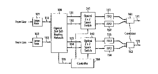
s Referring first to Fig. 1, there is shown an cptical (2x2) ATM
6 (asynchron~ls transfer mode) switchin~ system according t~ a first
7 embodiment of the present invention. Incoming e!ectrical pac~ets, or ATM
iS CPI15 of 53-~yte length are input to line interface units 10~ and t02 of the
9 switching system where ttleir celi he~ders are analy~ed by an incoming
header translator 103 (Fig. 1 a) and converted to optical signals by an
1 1 electrooptical converter 104 and applied to an optical header generator
1 7 1 OS. The optical switching system of this inventicn defines an opt;cal
13 header preceding each ATM ce!l. The optical he~der is e~iualiy s~parated
14 into time510t5 which are synchronized with system timing and l~niquely
1~ assigned to dif~erent destinations. Tne hea~er translator 1~3 is
16 synchroni~-d with the sys~em timing to produce an output signal in~ic3tlng17 the position Gf a tirneslot int~ which an optic~l he~der bit is to be
1~ inserted .or routing purposes in ~ccordanc~ with the a~alysis of a
19 destination code contained in the receiYed ATM ceil. The tirneslot
indicat~ng signal is output to the optical h~ader generator 105 to ~llcw
2 1 inse~ion of an opticaî header bit into the indkated position of an opticai
22 he3der that precedes the opticai ATh~l cell from the E10 converter 104.
2 3 The cutput sign31 from the header gene~ator 1 C5 af e3ch int~.~face unit is
21 therefore a series of an optical header and ~n o~tical j3-byte AT~1 cell,? 5 and is delivered as an output of the interface unit. The outputs of inte~race
2 ~ units 101 and 102 are respectively coupled via light waveguides 111 and
27 112 to respective inle~s of an optic~i ~2x4) seif-routing net~wor~ 120 in which
2 g they are switchcd, or transferred to one of its outl~ts which are coupled to
? ~ w~vesuides 1 3t - 134. Wavegui~es 1 31, 132 are connected to respective
3 0 inle~s of a conventional optical ~2,Y2) sp~ce s~itch 141, and waveguides
NE~80 - 6 ~ 0 8 4 1 5 ~
133, 134 are coupled to respec~ve inlets of an cptic~l (2~2) spac~ s;witch
2 142.
Each of these ~2x2) spacP switches is controlled in response t~ a switching
4 si~nal supplied from a controiler 180 to alternately ~sequentially) select
5 one of its out3ets to establlsh a switched path be~we~en the in)e~ to which the
6 aptical signal frcrn the precedinc stage appear; and th~ selected outle~
7 As will be desaibed, ~ontrolle~ 180 re~eiv~s a rou~ing signal via a signal bus8 170 from the se~f routing networ~ 120 .o generate the swltching signal for
9 couplin~ to the space switches 141, ~42.
1 o The autle~s of the spac~ switch 141 are co~lnected to optical ~irst-in-f,rst-
aut (FlF0) ~uffer mem~ries 1~1, 152 whose outpu~s are combined by an
optical combiner 161 onto an output waveguide 171. L.~ewise, the outlets
of the space switch 1 d2 are connected to optîc"l rlFO bu~er memories 153,
whose outputs are combined by an optic~l combiner 16~ onto an
15 output waveguide 172. In this way, cells are queued in the respective
6 bufler memories 15~ ~ 154 .o avoid possible o~itput contenticn with other
cell5 bound far th~ same destination.
1~ As shown ~n F~g~ 2, the ~2x4) sP!f-routing networ~ 12~ cor~pr~seS o~cai
1~ splitters 201 and 202 to which the waveguides 111 ana 112 are
respectively terrninated. The optical AT~1 c~li ;upplied thrcugh the
~1 waveguide 111 ar~ spl~t by splltter 201 ~nto ~WQ identic~l signals which are
~2 led to optical gat s 21 1 and 213 whose output tenninals are connected via
2, waveguid~s 131, 132 to the respective inle~s of the (2x7~ spac~ swi~c.~ 141.
24 In like manner, the optical cell on supplied through the wave~uide 112 is
2 5 spli~ by splitt~r 2û2 inw identical signals which ar~ led tc Gptical sates 212
~6 and 21~ whcse outpu~; are connected ~o waveguides 134 and 13~,
7 respectivefy. An electrical pulse generator ~50 is provided ,or ~pplying a
first voltage contro~ pulse 301 (see F,g. 3) to the control e~ectrode of optic~lgates 211 3nd 212 via resistcrs 22~ and 222, respective!y, and a sec~nd
3 o volt~ge con~ro~ puise 302 to optic~l gates 213 and 214 via resist3rs 223 and
~J
NE480
F ~084 ~ ~
- 7 -
224, respectively. Voltage sensors 231- 234 are connected respectively to
2 the control electrodes of optical gates 211 to 214. As described belo~, a
3 signif~cant voltage drop occurs at the control terminal of each aptical ga~e
4 as a result of a current passing through the ~ssociated ~esistor when the
5 header bit of an incident optical signal is time-coincident with an initial high
6 voltage portion or header of a voltage pulse applied to t~e gate. The
7 voltage drop developed at each o~ these optical ~ates is detected by the
8 associated voltage sensor. On detecting a voltage drop, v~ltage sensors
9 231 - 234 pr~duce respective output signals on control signal lines 241 tc
10 244 which are bundled to form the signal ~us 170 to the controller 180.
11 As illustrated in Fig. 3, the header of each voltage pulse applied to the
2 associated optical gate triggers it into a light transmissive state upon
13 coincidence with the routing header bit of an incident optical signal while
14 consuming its light energy and the pedestal portion of the voltage pulse
5 that follows maintains the gate under the transmissive state to allow the
6 data portion of the optical signal to pass through it. Therefore, on leaving
17 the optical gate, each optical signal loses its routing header bit and only
8 the data portion of the ATM cell appears at the output of the gate.
1 g More specKically, vol~ge pulse 301 rises from zero amplitude to a
20 highest amplitude VH at time tl and drops to a lower level, or pedestal VL
~ 1 at t~me t2 and drops to zero at time t6, wh~le voltage pulse 302 rises from
22 zero amplitude to the highest amplitude VH at time t~ ~nd dtops to the
2 3 pedestal YL at time t3 and drops to zero at bme t~. Each ATI~ cell has a
4 routing header bit that e~tists during a time slot between tl and t3, foltowed~5 by a series of 53 byte data bits that exist between t4 and t~. It is assumed
26 that that cells A and C are originated from ~ same or different sources
27 during firs~ and secont intervals, respect~vely, and multiplexed onto the
2 ~ waveguide 111, and cells ~ and D are likewise originated during the first
29 and second intelvals, respectively, and multiplexed onto the waveguide
3 o 112. For the purpose of illustration, assume that the routing header b;ts Ra,
NE480 - 8 - ~ 2 0 8 4 1 ~ ~
Rc and Rd of ATM c~!ls A, C and D occur durirlg the same timesiot tl-t2 af
2 the header inte~al ~ 3 and the routing header bit R~ of cell B oc~urs
3 during timeslot t2~
4 Since dle heade~ bit Ra is time~oincident with the he3der of voltage
pulse 30~ applied t~ gates 211- and 212, the data port:ion Da of cell A is
6 passed through gate 211 to waveguide 131, and the he~de~ bit R~ is tim~
7 coincident with the heade~ of voltage pulse 302 applied to sates 213, 214,8 the data portion Db of cell B is passed through gate 214 to waveguide î 34.
9 In like manner, the he~der bits Rc and Rd ~re respectively time-coincidentwitll the header of voltage pulse 3G1. Thus, the ~ata por~iolls ~c and C)d
1 1 of cells C and 1: ~re passed through ~atcs 211 and 212 respectively to
12 wavesuides 131 and 132. Therefore, depending on the time5~0t pasiti~n
3 cf their header bits, ~,e optical cells incident on spli~.er 2~1 are routed to
14 waveguide 131 or 133, and the optical cells incident on spliKer 202 are
routed ;o waveguide 132 or 134.
When cell A is ~assed through gate 211, the volt~ge sensor 231
17 produces an cutput that l~ coupled throush contrcl line 241 to th~
} 8 controller 1~0 as a routing signal indicating that a cell is routed to the upper
19 inlet of space swi~ch 141. Likewise, when celi O Is passed through gate
0 212, the voltage sens~r 2~2 produces an output that is coupled thr~ugh
21 control line 242 to the controller 180 t~ Indic~te that a cell is routed to ~he
~2 lower inlet or space switch 14t. Thus, the routing signals at control lines
3 243 and 244 in~ic~te that cells are routed to the upper and lower inle~ Gf
21 switch 142, respe tively.
The con;roller 180 uses ~he routing signal as an indication of the
location of a cell at ~ne cf the inle~ of t~e space switches141 and 142 to
~7 supply a switching signal to one of the switches 141 ~nd 142 which is
indicated by t~le routing signal to est~bllsh a path be~ween the
~ ~ inlet i~entified by the routing signal and one of the cutle~s or the (2;c2)
spaceswitch and the cell is qtleued in che FlFO buffer memo~r coupled ;o
I'~E~80 2 0 8 ~
g
that space switch.
2 With the output ~ueuing (~uf~e~ pr~nciple of the present invention, the3 (~x~) ATM switching system of the first embodiment of this invention
4 requires only two ti~ne slots. This represents a reduction of the number of
optical header timeslots required for self-routing purposes in comparison
6 with four t~meslo~s required with the prior art (2x2) lnput buffer ATM
switching system, and hence, the throughput of an optical (2x2) ATM
8 switching systern is increased by a f~ctor of 2. With N x N output buffer
9 switching systems of this invention, a reduction of header timeslo~s by a
10 factor of N is achieved.
11 The same timeslot ~eduction effect is equally achieved by the
12 embodlments which will be described below.
13 In the second embodiment of this invention, shown in Fig. 4, optical
14 ATM cells are carried on different wavelengths when the corresponding
electrical cells are processed by the respective interface units 401 ~nd 402,
16 and the rout;ng network 120 and (2x2) switches 141, 1~2 of the previo~
11 embodiment ~re replaced with an optical (2x2) self-routing network 420,
1 8 splitters 441,. 442 coupled by waveguides 431 and 432 to the outlets of
1~ network 420, and w~velength tunable f~lters 451 to 454 coupled to the
2 0 outputs of splitters 441, 442. The wavelength of optical ATM cells A and C21 is designated ~1 and the ~avelength of the other cells is desigr~ated ~2.
2 2 As shown in Fig. S, the (2x2) self-routing network 420 differs from the23 routing network 120 of the first embodiment by the inclusion of an optical~4 combiner ~1 for c~mbining cells from optical gates ~1~ and 512 for
2 ~ couplin~ to waveguide 431 and an optical comblner 56Z for combinlng
cells f~om ~a~es 513, ~14 for coupling to wa~eguide 43~. If the incoming
27 cells occur in the same time intervals as in Fig. Z wi~h the sarne optic~l
28 headel timeslot positions coincidlng with the same voltage control pulses
2 ~ as those in Fig. 2 as illustrate~ in Fig. 3, cells A 2nd ~ ap~ea~ at waveguide
3 0 551, cell C) appears at waveguide 552 and cell B appears at waveguide 535
~ 2 ~ ~ 4 1! 5 ~
- 10-
in the same way as in Fig. 2. Cells A and C are therefore time multiplexed
2 onto waveguide 431, and cells C and D are wavelength multiplexed by
3 combiner 561 onto waveguide 431 and applied to the splitter 441. On the
4 other hand, cell B is applied to the splitter 442 without being multiplexed in
any form with other cells.
6 Returning to Fig. 4, each of the cells A, C and D, on entering splitter 441,
7 is split into replicas of the cell, which are applied respectively to the
8 wavelength tunable filters 451 and 452, while cell B is split by splitter 442 into
9 identical signals for coupling to the wavelength tunable filters 453 and 454,
respectively. Controller 480 produces a wavelength tuning signal that enables
11 each wavelength tunable filter to selectively pass one of wavelengths ~11 and
12 ~12 and applies it to one of the wavelength tunable filters. The generation of
13 the tuning signal and the application of this signal are determined in
14 accordance with a routing signal supplied via signal bus 470 from the (2x2)
self-routing network 420. The outputs of wavelength tunable filters 451 and
16 452 are supplied to FIFO buffer memories 461 and 462, respectively, whose
17 outputs are combined by combiner 471, while the outputs of wavelength
18 tunable filters 453, 454 are supplied to FIFO buffer memories 463, 464,
19 respectively, whose outputs are combined by combiner 472. For example, by
tuning the filters 451 and 452 to wavelengths ~11 and ,12, respectively, cells A21 and C are sequentially stored into memory 461 and cell D is stored in memory
22 462.
23 Fig. 6 is a block diagram of a third embodiment of the present invention in
24 which an optical (2x4) ATM switching system is illustrated. This embodiment
utilizes wavelength multiplexing to reduce the number of the timeslots for the
26 optical routing header bit of the (N x M) ATM switching system to 1/9 of the
27 number which would otherwise be required for an optical (N x M) ATM
28 switching system of input buffer type.
29 In Fig. 6, the (2x4) switching system includes an optical (2x4) self-routing
network 620 which sequentially receives incoming cells A, C and E
~ . ,
NE~80 2084102
11
of different wavelengths thr~ugh waveguide 611 and cells 3, D 3nd F of
different wavelen~ths through wave~uide 61~. The outlets of self-routing
3 network 620 are coupled respectively through waveguides 631 - 634 to
4 optical splitters ~41 - 644 each of which splits the input signal into two
5 identical signals for coupling to a corresponding one of w~velength tunable
6 filt~rs 651 - 658 whose ou~puts are coupled respectively to optic~l FIFO
7 buffer me~nories ~61 668. The memories 661 ~ 6G8 are folmed into four
B pairs corresponding respectively to combiners 671 - 674 and the outpu~s
9 of the memories of ea~h pair are combined by the correspon~ing
10 combiner to appear at one of QUtpUt waveguides ~81 684. ~ontroller
11 680 is responsive to a roUt~ng signal from the ne~work 620 for generating a
L2 waveiength tuning sign~l and applying it to one of the wavelength tunable
13 filters 651 - ~58 in a manner simil~r to the second embodiment.
4 In Fig. 7, the optical (2x4) sel~-routing network 620 con~prises a first
1~ optical splitte~ 701 for splitting each incoming cell on waveguide 611 into
16 four identical optical outpu~ for coupling to optical g~tes 71 1 714, and a
17 second optical splitter 701 for splittin~ e~ch incoming ~ell on waveguide
1 8 612 into fou~ identical optical outputs for coupling to optical gates 71 S -
19 718, respectively. Optical ~a~es 711 - 714 form pain with optical gates 715
20 ~ 718, respectively, and the outputs of the paired ~tes afe coupled to
2 1 combiners 731 ~ 734 whose outputs are connecte~ thro~Jgh wavegui~es
22 631 634 to the splitters 641 - 644. Electrical pulse generator 750 drives
23 the paired gates with correspondlng voltage pulse$ 801 - 804 through
24 resistols 721 ~ 7Z8 connected to gates 711 - 71B, respectively. The
25 ~ontrol electrodes of these optical gates are coupled to respeçtive voltage
2~ sen~ors 760 whose outputs connected to the controller 680.
~7 The operation of the ~Zx4) self-routing network of Fig. 7 is as follows.
28 Assume that the header of volta~e pulses 801 and 802 occurs durin~ the
29 s~me timeslot t1-t2 which coincides with the po5ition of -the routing header
3 0 bit of cells A (~ 22) and C(~21), and the header of voltage pulses
~IE480 208~ 102
803 and 804 occ~rs during the same timeslot tz-t3 whlch coincides with the
2 position of the routing header bit of optic~l cells D (~12), E (A~1) and F
3 (~22). Cells A, C ~nd E are assumed to occu~ sequentially during first,
4 second and third successive intervals, and cells B, D and F are assumed to
5 occu~ ~uring. the same first, second and th~rd intervals, respectlvely. It will
6 . be seen that.cell A on w~vegulde ~11 is switched thro~gh gate 711 and
7 ~ppears at wave~ui~e 631 as its routin~ header bit coincides with the
8 header of pulse 801, and cells B and C on respective waveg~lides 61~
9 ~re switched through gates 716, 712, respectively, and time multiplexed by
10 cornbiner 732 onto waveguide 632 as ~heir routing he~der bits coincide
1 I with the hea~er of vol~age pulses 802. Likewise, cell D on wave~uide 612 is
12 swi~ched through gate 717 and appe~r at waveguide 633 as its routing
13 header bit coincide with the header o~ pulse ~03 and cells E ~nd F on
14 waveguides 611 and 6~2 are switched throu~h gates 714, 718,
1 s respectively, and wavel~ngth mul~iplexed by combiner 734 onto
1 6 waveguide ~34.
17 It is seen that only two timeslo~s are required for the optical header bits
18 of this embodiment, a nurnber which is 1/4 of that which would otherwise
1~ be required for ~n equi-~alent optical (2x~ ~TM switching system of input
2 o buffer 'lype.
21 The throughput of op~ic~l AT~ switching systems u~ing optical routing
22 headers can be in~reased by so~ting incomin~ optical ATM cells between
23 ~vo or more self-routing networks. For this purpose, ~ fourth embodirrent
~ 4 of the present invention is shown in Fig. ~. Incoming electrical ATM eells
25 are entered to interface units 901 and 902, the outputs ~f which are
2~ respectively coupled to (1x2) sorters 911 and ~12. Each of the so~ers 911,
27 912 h3s two outputs respectively connected to respective inle~s of optical
x4) self-routing network~ 921 ~nd 97~ of configuration identical to the
2 ~ network 620 of Flg. 7. In e~ch interface unit, the cell he~der of each cell is
3 o examined ~y a he~der translator ~03 ~Fig. ~a) to generate a routlng
~IE 180 2084102
- 13 -
header position si~nal and ~ sor~ing signal, while the cell is converted to
2 optical form by an ~/0 converter ~04 and fed to an optical header
3 generator ~05. Header generator 90 responds to the routing header
4 position signal by inserting an optical header bit in the sarne manner as
described earlier. The output of optical header generator 90~ is applied to
6 an optical sorter gl l (912) to which the sorting signal from translator 903 is
7 also applie~ for sortin~ the incorning cells to one of the self-routing
8 networks.
g E~ch of the self-routing netw~rks ~21, 9~2 has four outle~s coupled to
respective inputs of combiners ~31 ~ 934. The outpu~s of combiners 931,
11 932 are connected to respeCtiYe input~ of an opt;cal (~x23 space switch 941 2 whose outputs are tonnected through buffer memories 951, g52 to
combiner 961, and the outputs of combiners 933, ~34 ar~ connected to
14 reSpective inputs of ~n optical (2x2) space switch 942 whose outputs are
1 s connected through buffer memories 953, 954 to combiner 962.
1~ ~ontroller 980 receives a routin~ slgnal from both self-routing networks
l 7 to control l:he (2x2~ space switches 941, 942 in a mannel similar to that
l ~ shown and descri~ed with reference to Fig. 1.
1 ~ The operati~n of the embodiment of Fig. g will be described with
20 reference to Fig. 10. Assume that electrical ATM cells D1, D2, and ~3
~1 bound for the same destination successively arrive at inter~ace unit 901
2 2 during intervals tl-t2, t2-t3 and t3-t4 and cells D1 and D3 are sorted to
2 3 network g21 while cell D2 is sorted to ne~work ~22. Puring int~n/a~ t1-t2, the
2~ header of electrical cell Dl is examined by translator 903 and an optical
25 routing bit Hl is generated and appen~ed to the optical ver~ion of cell D1
2 6 that occurs during inte~al t2-t3 and is sorte~ to network 921. Similarly, the
27 header of electrical cell ~2 is examined during interval t;~-t3 and an optical
Z g routing bit H2 is generated and appended to the optical version of cell D3
29 that occurs during int~rval t3-~ and is sorted to network g22. The header
3 o of electrical cell ~3 is examined during the next interval t3-t4, and an optical
NE-480 208~1~2
- 1 4 -
routing bit H3 i5 generated and appended to the optic~l ve~sion of cell C)3
2 that occurs during interval t4-ts and is sorted to network 9~1. In each
3 network, the cells a~e routed in a manner as described so that their routlng
4 header bits are consumed and the data bits o~ cells D1, D~, D3 are directed
5 to the s~me combiner ~1, hr example, so that the cells separated by the
6 sorter 911 are recombined at the output of combiner 931. By the sorting
7 oper~tion, the transfer of a header-appended cell to the appropri~te
g network can ~e per~ormed simul~aneously with the appending of an optic~l
routing bit to ~he next cell, and the cells can be processed by networks ~21
10 an~ 922 in parallel f~shion. Therefore, switched cells C)1, 1~2 and D3 are
l l closely spaced in time sequence at the output of combiner 931 between
12 times t1 and ts as illustrated in Fig. 10. Otherwise, incoming cells must be
13 put In a queue to append a routing bit and as a result, it would require
l 4 additional two slot intervals to complete the switching of cells D1, DZ and
15 ~3.
1~ An alternative form of the fourth embodiment of this invention is shown
17 in Fig. 11 in which the sorting technique is combined with the wavelength
1~ division multiplexing of Fig. 4. ~;)ptical cells of waveleng~h ~1 are inp~t to
1 9 1 x2 sorter 111 1, and optical cells of wavelength ~2 are input to 1 x2 sorter
20 111 2. The outputs of each s~rter are couple~ ~o respective inl~ts of (2x2)
2 1 self-routing networl~ 112~ and 1172. ~ote that sorters 1111 and 1112
27 handle AT~l cells of wavelengths respectively assigned to the sorters. The
23 two outlets of each self-routing network ~re couple~ to respective inputs of
24 combiners 1131, 1132 whose outputs are input to splitters 1141, 1142,
2s respectively. Wavelength tunablefilters 1151 - ~154 are connected to
2 6 respective outputs o~ splitters 1 141, 1142 to selectively pass desired cells to
27 bu~fer memories 1161 ~ 1164 under control of controller 1180 in response
28 to a ~outing signal from netw~rks 1121 and 11~2. The outputs of buffer
2 9 memories 11~1 - 1164 are coupled in pairs to combiners 1171, 1 172 as
3 o illustrated.
NE~80 20841132
- 15 -
Another alternativ~ form of the fourth embodirnent of this In~ention is
2 shown in Fig. 12 in ~,vhich the sorting technique i5 combined with the
3 wavelength multiplexing of Fi~. 7. Optical cell5 of wavelengths ~ 71 are
4 input to sor~ers 1211 and optical cells of wavelength ~12, ~22 are input to
5 sorter 1212. ,The outputs of sorter 1~1 t are coupled to respective iniets of
6 (2xJ,) self-routing networks 1~21, 1~22, the two outlets of each network
7 being coupled to respective inputs of combiners 1231 ~ 1234 whose
8 outputs are input to splitters 1241 ~ 1 ~J.4, re$pectively. Wavelength
tunable filters 1 ~51 - 1258 are connected to respective outputs of ~plitters
1 0 1241 1244 to selectively pass desired cells to buffer memories 1~61
1 1 1268 under controt of controller 1780 in response to a rout~n~ sign~l from
12 networks 1~21 and 172~. The outputs of buffer memories 12~ 8 are
13 connected in pairs to combiners 1271 ~ 1~7~.
14 A fifth embodiment of the present inventlon is shown in Fig. 13 in which
1 ~ the system receives ATM cells of different priorities and priority control is
16 perFormed when output contention occurs between cells of different
17 priorities. In Fig. 13, high-priority electrical ATM cells A are input to
18 interface unit 1301 and low-priority electrical ATM cells B are input to
1 ~ interface unit 1302, Each of these interface units examine the dest~'nation
20 identifiers contained in the received ATM cells and ~enerate an optic~l
21 routing bit in a manner as described, and f~ther examine the priority bit~
2 2 to generate an optical so~ting bit and an optical priority bit as shown in Ftg.
23 14. In a typical example, to optical cell A the interface unit 1301 appends a2 4 routing bit Ra during ~imeslot tl -t~, a sorting bit Sa during timeslot t3-t4, and
a high prio~ity bit Pa during timeslot ts-t~, and ~o optical cell B the interface
2 6 unit 1302 appends a ~outing bit Rb during timeslot ~-t3, a sorting bit Sb
27 during timeslot t4-t5, an~ a low priority bit P~ during timeslot t5-t6. In each
2 8 cetl, data bits sta~ at time t7 and terminate at time t8. Priority bit Pa has a
2 9 higher light intensity L1 than the light intensity L~ of priori~ bit Pb.
3 0 An optical (2x4) self-routing networ~ 13~0 is provided for receiving
NE~80
208~1~2
- 16-
optical cells from ~he interface units 1 ~01, 1302 for routing them using
routing bi~s Ra an~ Rb to opticai (2x2~ spa~e swltches 1331 and 1332 where
3 they are switched to one of their output terminals under control of
4 controller 1380 in a mannel identical to that ~escribed in connection with
Fig. 1. The outputs of (7x2) space s~itch 13~1 3re connected to priorit!y
6 sorters 1341 and 1342, respectively. Each of these priority sorters has a
7 high priority output terminal and a low priority output terminal and is
8 controlled in response to voltage pulses supplied from an electric~l pulse
g generator 1350 to set up an optical path to one of tts output terminals
10 according to the sortin~ bit of a cell it receives frorn the associated space11 switch in a rnanner as described in detail belo~.
12 FlfO buffer memories 1~51 - 1358 ~re provided. These buffer
13 memories are ~rouped into four pairs respectively corresponding to sorters
1341 - 1344 and the memories of e~ch pair are connected to the outputs
15 of the corresponding sorters. Therefore, the buffer memories connected
1~ to the high priority output ~erminals of the sorters receive only high priority
1~ cells A and those connected to the low priority output tenninals receive
8 only low priority cells B. rhe outputs of high priority mernories 1351 and
19 1353 are conn~cted to the inputs of a combiner 1361 anc~ the outputs of
20 low priority memories 1352 and 1354 2re connected to the inputs of a
21 combiner 1362, the output of these combiners being connected to a
2~ respective input of a priority gate 1~71.
2 3 In a similar mann~r, the c~utputs of hlgh priority rnemorie~ 1355 and
24 1357 are connected to the inputs of a combiner 13~3 and the Outpl~ts of
5 low priority memories 1 3S~ ~nd 1358 are connected to the inputs of a
26 combiner 13~4, the output of these combiners being corlr~ected to a
~7 respective input of a priority gate 1372. Each of the priority gates 1371
~8 and 137Z receives a voltage pulse from the pulse g~nerator 1350 to pass
2~ high priority cells to the output of the gate when contention occurs with a
3 o low priori~ cell at the inputs of the gate in a manner as will be de~cribed
NE480 2 0 8 ~
later.
2 As shown in d~tail in Fig. 15, each of the priority sorters comprises an
3 optical spiitter 1500 hsving two outputs, and a pair of optical gates 1501
4 and 1~02 connected respectively to the outputs of splitte~ 1500. Each
optical gate is ~ri~Jen by a different voltage pulse supplied from the pulse
generator 1350. As shown in Fig. 16, a volta~e pulse 1601 having a
header during inte~al t3-t4 and a pedestal portion terminatl'ng at time tg is
8 applied to gate 1501 and a volta~e pulse 1602 having a h~ader during
interval t4-tS and a pedestal termi~atin~ at time tg is applied to gate 1502.
10 Since the high-priority cell A has consumed its routing bit Ra as the cell is1 1 swikhed by the self-routing network 1320, it contains the sorting bit Sa and12 prior;ty bit Pa. The sortlng bit Sa of the signal applied to gate 1~01
3 coincides with the header of voltage pulse 1601, and so its ~at~ bits are
14 allowed to pass through gate 1501 to the high-priority output of the sorter,
1~ while the ~ata bits of the other input to gate 1502 are rejected. Likewise,
1~ the low-priorit~y cell 3 has consume~ its routing bit ~b as it is switched by17 the self-routing network 1320, it contains the sorting blt Sb and priority bit
18 Pb. When either of cells A and B is applied to the sorter, it is divided into1 g identical signals by splitter 1500 and applied to gates 1501 and 1502,
20 respectTvely. Sin~e the sorting bit Sa of cell A applied to gate 1501
~1 coincides with the hea~e~ of voltage pulse 1601, the data bits th~reof ate
22 allowed to pass throu~h gate 1501 to the high-priority output o~ the sorter,
23 while the data bits of cell A applied to gate 1502 are no~ allowed to pass
~4 through it. On the other hand, the sorting bit Sb of cell B applied to ~ate
25 1 S02 coincides with the header of voltage pulse 1602, the data bits thereof
2 ~ are allowed to pass through gate 150~ to the low-priority output of the
27 sorter, while the dat~ bits of cell B applied to gate 1501 ~re not all~wed to2g pass thlo~Jgh it. In this wzy, cells of different priority leYels are sorted
2 9 according to the timeslot position of their sorting bits in rèlation to the
3 0 timeslot position of the applied volt~ge pulse.
~Y
N~ i80 208~10~
Details of the priority gates 2081, 7082 are shown in Fig. 17. Each
priority gate comp~ises a pair of optical ~ates 1701 and 1702 ~r recei~ing
3 a high-priority rells and ~ low-priority cell from the associated combiners,
4 respectively. Pulse generator 1450 supplies a voltage pulse 1801 through a
s resistor 1703 to the control electrodes of these g~tes (Fig. l 8). The outputs6 of ~ates 1701 and 1 70Z are cornblned by a combinel 1704.
7 As shown in Fig. 18, the headef of this voltage pulse has amplitude \IHo
8 and occurs during interval tS-t~ coincident ~ith both priority bit~ Pa and Pb,g ~nd the pedestal portion of this pulse has amplitude VLO and terminates at
10 time t~. If contention occurs at the inputs of the priority gate be~een a
11 high ,oriority cell A an~ a low priori~r cell B, the cell A has only the priority
bit Pa as it has consumed it~ sorting bit Sa in the previous stage, and the
l 3 low-priority cell B has likewise the priori~ bit Pb only. Since priority bit Pa
14 has a higher intensity than priority bit Pb, g2te 1701 is tri~gered into
l 5 transmissive state, c~using a current to flow through the conducting gate,
16 and hence ~ voltage drop across resistor 1703. Thereafter, the heade~ of
the voltage pulse applied to ~oth optical gates 1701, 170~ ~educes to tevel
l 8 VH1 and the pedestal to VL1 as indicated at 1802 which is suf~icient to
1~ maintain its transmissivity to pass the data portion of cell A through gate
2 0 1 7û1 to be delivered throu~h combiner 1704 to the output terminal.
21 An altemative form of the p~iority gating operation is shown in Fig. 19.
2 2 The hi~h priority cell A is appended ~ith a priority bit P'a that occl~rs
2 3 during interval ts-t6, and the low priority celi B is appended with a priority
~4 bit P'b that occurs during interval 4-t7, with both priority blts being of equal
light intensity. The data bits of each cell exist during inter~al t8-tg. The
2~ pulse generator 1450 supplies a volta~e pulse 1gO1 to resistor 1703 with
~7 he~der with amplitude ~IHO th~t lasts between times t6 and t7 and a
2 8 pedestal portion with amplitude VLO that terminates at time t1 o. ~ince
~ priori~,r pulse P'a is earlier than P'b when contention occurs between ~ells
3 0 and B at the priority gate, optical gate 1~01 i5 triggered, causing a current
NEq80 208~102
- 19 -
to flow through resistor 1703, so that the header of the voltage pulse
2 applied to both ~ates reduces to level V~l and the p~ele~tal po~tion of the
3 pulse to level VL1. as indicated by ~ pulse 1902.
4 An alternative form of the f~h embodirnent of this inven~ion i~ shown in
5 Fig. 2~ in which priori'y selection is combined with the wavelength di~tision
6 multiplexing of Fig. 4. Electrical high-priori~ cells A are input to inter~ce
7 2001 where they are converted to optical signal of wavelength ~1 and
8 applied to (7x2) self-~outing network 2020 ~nd electrical low-priority cells B9 a~e inp~t to interface 2002 where they are converted to optical signals of
0 wavelength ~2 and applied to the network. Each outlet ~f netvvork ~020 is
11 connected to a splitter 7031 ~2032) having two outputs respectively
12 connected to wavelength tun~ble filters ~041, 7042 (2~43, 20~4), the
3 outputs o~ filters ~041, 2042 (2043, Z044) being connected to sorters 2051,
2052 ~2053, 2054), respectively. Sorters 2051 - 2054 are responsive to
15 volt~ge pulses supplied from ~lectrical pulse generator 2030 to sort the
16 high priority cells to FIFO buffe~ memories 20~1, 20~3, 20~5, ~0~7 whose
17 outputs are connected to combiners 2071, 2073 and the low priority cells
1~ to memories 2062, 2064, 2066, ~06~ whose outputs are connected to
combiners 207Z and ~074. Priority gate 2081 is connected to the outputs
~0 of combiners 2071, ~072 ~nd priority gate 2082 to the outputs of
21 cornbiners 2073, 2074 to provide prio~ity selection when contention oc~urs.
22 In another alternative form, the prionty selection fe~ture of the fifth
23 em~odiment can be combined with the wavelength multiplexing of Fig. 7
~4 as shown in Fig. 21. Optical cells o~ different priorities with wavelen~th ~1 t,
5 ~21 are input to one inlet of (2x4) self-routing network 2120 3nd optical
~6 cells of different priorities with wavelength ~12, ~22 are input to the other27 inlet of the network. Each outlet of the (2x4) network 2170 is connected to
~ 8 a splitter 2131 (713~ - 2134) having ~o ou~puts respect~ely connected to
2 ~ w~velength tun~ble filters ~141, ~142 (2143 - ~148), the outputs of filters
30 2141, 2142 (2143, 2144) being connected to sorters 2151, 2157 (2153 -
,y
NE~80
~081102
- ~o-
~ 158), respectively. Sorters 2151 ~ ~158 are responsive to voltage pulses
2 supplied ~rom electrical pulse ~enerator ~t S0 to sort the hi~h priority cells3 to FIF0 buffer memories 2161, 2163, 2165, 2167, 21 6~, 2171, ~1 73, 2175
4 whose outputs are onnected to combiners 2181, 2183, 218~, 2187 and
s sor~s th~ low priority cells to memories 2162, 2164, 2t 6~, 2168, 2t 70,
2172, 7174, ~176 whose outp~ts are connected to combiners 7182, 2184,
7 ~18~, 2188. Prioriy gate 21 g1 (Z192, 2193, 2194) is conn~c~ed to the
outputs of combiners 2181, 2182 (2183~ 2188) ~ provide prioriy selection
g when contention occurs.
10 A sixth embodlment of the present invention is shown in Fig. 22. In this
11 embodiment, an optical (2x2) copy network 2230 is provided in
1~ preceding stage o~ the optical self-routing network of the present inventio~
13 for multicasting an ATM cell to as many outlets of the self-routing network
14 as there are routing (copying) bits contained in the optical header of the
15 cell. AS illustrated in Fig. 22, the system includes interface units 2201 and1~ Z~02 through which electrical ATM cells ~rom ~he açsociated transmission
1~ lines are received and conv~rted to optical form for coupling through
1 8 waveguides 2711 an~ 2212 to the copy network. The interface units are
19 connected to a multicast controller 2220 which ~enerates a multicast
20 control signal indic~ting the number of "copying" bits to be inserted to the
21 optical header of ATM cells as ~ell as the timeslot positions of the copying
22 bits in the optical header. As illustrated in Fig. 23a, each inter~ace unit iç
~3 comprised of an eiectroopticai converter 2310 connected to a coaxial cable
24 through which it receives incoming signals and converts them into optical
~5 signals. An optical header generator 2320 ls coupled to the E/0 converter.
~ 6 In response to a multicas~ ~ontroi signal from multicast control~er 2220, the
27 inter~ace unit inserts optical copying bits in the indicated timeslots of the28 header of an optical AT~ ~ell and forv~a~ds it to the copy network 2230. If
29 the transmission medium is optical fiber, an optical buffer men~ory 2330 is
3 0 used ~see fig. 23b). Such optical buffer memories ar~ ~escribed irl a papef
,~
~IE ~180 2 0 ~ 4 1 ~t ~
titled "Ph~ton,c ATI~I Switch Using Ver~ical To Surface Transmission Electro-
2 Photonlc De~ices (VSTEPs), Makoto Nishio et al., The XIV International
3 Switching Symposium, Proceedings Vol. 2, October 25-30, 19g2,
4 Y~kohama, Japan.
The outputs of copy network 2230 are coupied respectively to
6 interface units 2241 and 2247 whose outputs are connected to an optical
7 self-routing network 2250 constructed according to the present invention.
8 As illustrated in Fi~. 24, the (~x2) optical copy network 2230 comprises
g (1 x2) splitters ~401 and 2402 connected to the waveguides 2211 and 2~12,
1 0 re~pectively. The outputs of splitter 2401 are connected to optical gates
1 1 2411 and 2413, respectively, and the outputs of splitter 2402 are connected
12 to optical gates 241~ and 2414, respectively. A pulse generator ~440
13 supplies ~ first voltage pulse through resistor 2421 to the control electrode~
of optical gates 2411 an~ 2~13 ~nd 3 second voltag~ pulse through resistor
2422 to the control elec~rodes of optical gates 241~ and 2414. The outputs
1~ of optical gates Z411 and ~412 (2413 and 2414) are connected to a
17 ~ornbiner 2431 ~43~) whose output i5 coupled to an in~erface 2~41 (2242).
1 g A typical. example of the volta~e pulses and optical cells appearing in
19 Fig. 24 is shown in Fig. 25. The optical header of each cell is divided into
20 several ~imeslots and copying bits Cal and Ca2 are inserted into tin~eslots
2 1 t1-t2 and t3-4 of cell A on waveguide 2211, and copyinJ bits Cb1 and Cb2
2 2 are inse~ted into timeslots t2-t3 and t4-t5 of cell B on waveguide 2212. The2 3 header of the first voltage pulse 7501 applied to resistor ~421 from pul~e
24 generator 2440 occupies two consecutive timeslots tl-t3 and the header of
25 the second voltage pulse ~02 applied to resis~or 2422 occupies two
2 6 consecutive timeslots t3-t5. If optical cell A Is incident on the input of splitter
27 2401 during ~ given ATM frame inte~al, the copying bits Cal and Caz
2 ~ coincide with the respect've headers of voltage pulse~ 2501 and 25~2
9 applied to resistors 2421, 2422. Optl'cal gates 2411 and 2413 are d~iven
3 0 into li~ht transmissive sta~e to allow cell A to be passed to combiners Z431
I~E480
2084~02
- 22 -
and 743~, so that copies of cell A are forwarded to inteRace units 2241 and
~24~, respectively, while d~wing cu~rents through resistors 7421 and 2422.
3 As a tesult, the he~der of both voltage pulses reduce to a level too low for
4 the othel optical gates to turn on. With optical gates 2411, 2413 being
s rendered conductive, the voltage pulss applied to optical gates 2411, 24136 appears as shown ~t 25~3 and the voltage pulse applied to ~ates 2412,
7 2414 appears as shown at 250~.
8 If cells A and B are si~nultaneously entered to splitters 2401 and 2402,
9 contentions occur between coples of these cells at the inputs of optical
1 0 gates 2411 ~nd 241 ~ and at the inputs of optical gates 241 3 an~ 2414.
11 Since the copying bits of cell A are earlier than those of cell B, only copies
12 cell A are allowed to pass through optical ~tes 2411 and 2413 ~n
13 directed to interface units 2241 and 2242.
14 If the interface units 2241 and ~42 are identical to those shown and
15 described in connection with the embodiment of Fig. 1, they
16
17 insert routin~ bits R1 and R;~ in~o different timeslots ts-t7, for example, of the
1 ~ first and second copies of the incoming cell as illustrated in Fig. 25. The
19 copies of the cells are now launched into the self-routing network 2250 and
20 routed according to their routing bits in a m~nner as described in ~he
21 previous embodiments.