Note: Descriptions are shown in the official language in which they were submitted.
CA 02084303 2002-12-02
20104-8768
1
Low delay or low loss switch for ATM
The invention relates to a telecommunication
switching arrangement for switching digital data which are
contained in data cells provided with a cell header, the
arrangement comprising a crosspoint switch for switching
cells from an input line of the switch to an output line of
the switch, the switch being provided with a cell buffer
memory for storing the cells to be switched through.
Such an arrangement can be used for fast packet-
switching techniques which are known under the name of ATM
(Asynchronous Transfer Mode). The power of ATM is its
ability to provide bandwidth on demand: different sources
can have different bandwidth requirements.
Fast packet switching techniques clearly provide
the flexibility for integration of mixed traffic streams,
such as voice, data and video. Due to provision for the
stochastic bandwidth requirements of some traffic sources,
it is not so clear at first. sight whether a reasonable
degree of utilization of switching and transmission
resources can be achieved. That is, the primary benefit of
fast packet switching lies in its flexibility to serve
different traffic streams. The invention has for its object
to provide an ATM system that can serve different types of
traffic streams and which also uses capacity more
efficiently than known arrangements.
Thereto, one aspect of the invention provides a
telecommunication switching arrangement for switching
digital data contained in data cells provided with a cell
header, said cell header containing a cell loss priority
field for storing a value representative of a cell loss
priority of the data cell, the arrangement comprising a
CA 02084303 2002-12-02
20104-8768
la
crosspoint switch for switching incoming data cells from a
plurality of input lines of the switch to an output line of
the switch, the crosspoint switch further comprising a cell
buffer memory for storing the data cells to be switched
through, the improved arrangement comprising: (a) a cell
buffer memory comprising first and second memory areas, the
first memory area for storing first cells having a high loss
priority value and the second memory area for storing second
cells having aglow loss priority value, (b) determining
means coupled to the input lines for determining the value
in said cell loss priority field of the cell header of each
incoming data cell to determine whether its cell loss
priority is a high loss or low loss priority value, (c)
allocating means in said crosspoint switch for in response
to the determining means determining a high loss priority
value of an incoming first cell for allocating said incoming
first cell to the first memory area and in response to the
determining means determining a low loss priority value of
an incoming second cell for allocating said incoming second
cell to the second memory a--rea, (d) switching means in said
crosspoint switch for reading out for switching purposes
first the high loss priority cells from the first memory
area and for switching to reading out the low loss priority
cells from the second,memory area when the number of cells
stored in said second memory area exceeds a predetermined
value, wherein said determining means, in response to the
cell buffer memory being full, are arranged for storing
incoming second cells having a low loss priority value in
the first memory area by replacing first cells having a high
loss priority value stored therein.
CA 02084303 2002-12-02
20104-8768
2
The invention makes use of the insight that some sources require low delay .
variation whereas other sources require low loss probabilities for ATM cells.
From the CCITT'
Draft Recommendation L361: "ATM layer specification for B-ISDN", January 1990,
it is
known that the ATM cell header should have a CeU Loss Priority (CLP) bit. This
CLP bH
creates the possibility to distinguish between two types of cells.
The performance of the ATM network as exposed to the user, depends
primarily on the call acceptance probability. Known methods of resource
allocation usually
decide to accept an ATM connection if the resulting cell loss probability for
of the aggregate
input traffic remains below a preset maximum value. In these known methods the
expected cell
delay is considered of minor importance. Sometimes a higher cell loss
probability can be
tolerated, which then could be specified in the cell header, e.g. by using the
CLP bit. Hereby
two classes of traffic are introduced. The first class encompasses traffic
requiring low loss
probability. Traffic of the other class gives in on loss probability but gets
a lower delay
variation in return.
Sources that generate traffic whose time relation needs to be restored
after passage through the asynchronous transfer network , benefit from a low
delay variance.
This is so since delay dejirier buffers in the terminal equipment can be kept
smaller if the
trans-network delay variance is small. Traffic sources that generate traffic
for which the
integrity is of prime importance, on the other hand, w~71 prefer a low
probability of cell loss.
An example of the latter is (machine oriented) data traffic, an example of the
first is (human
oriented) audiovisual traffic.
With integrated circuit technology one can realize buffers for several
hundreds
of ATM cells on one chip. These buffers, together with on-chip control logic,
can be used to
implement LDOLL (Low Delay Or Low Loss) queues. An LDOLL queuing policy
favours low
delay (or high loss) cells in service priority and low loss cells in storage
priority.
To describe the sources of different traffic streams it should be realized
that a
cell transmission takes a few micro-seconds, a burst of cells (activity period
of a source) lasts,
wo ~ae19o6o ~~ret~t,gzeooa6~
3
say, a fraction of a second, and the connection between source ~~d ~ ~t~a~ can
stand for
a several minutes.
Connections do not always need the full bandwidth for the whole duration of
the connection. Moreover, the bandwidth requirement usually differs for the go
or return path
of a connection. Some traffic sources like some video coders have a variable
bit rate (VBR).
E.g. in the case of a file transfer, a burst of packets is transmitted.
Termination of the file
transfer does not necessarily imply immediate termination of the connection
because more data
may be exchanged subsequently. In the case of a VBR coder, the cell rate (i.e.
bandwidth)
may change every 1/25 s. (resp. 1/30 s.), once every video frame. With its
cell buffer array
the LDOLL queue can allow for short periods of overload. This could provide an
alternative
for burst blocking.
The invention will be further explained in the following with reference to the
drawing Figures, in which:
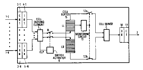
Figure 1 shows an embodiment of an ATM switching arrangement according
to the invention;
Figure 2 shows a graphical representation of the probability of loss of LD and
LL cells of the switching element according to the invention, compared with
a FIFO policy;
Figure 3 shows a graphical representation of the delay of LL and LD cells
compared with cell delay in a FIFO read-out policy;
Figure 4 shows a graphical representation of the probability of LL and LD cell
loss compared with a FIFO policy, dependent on a threshold value;
Figure 5 shows a graphical representation of the cell delay of LL and Ld cells
compared with a FIFO policy, dependent on. a threshold value.
Fig. 1 shows an ATM switching arrangement which might be considered the
elementary building block of an ATM network. The arrangement has N ATM input
links 1-1
through 1-N and one ATM output link 2. It is assumed that all links of the
switching
arrangement operate synchronously; the interval between two successive (idle)
cell arrivals is
called a time slot.
The cell receivers 3-1 through 3-N deserialize an incoming cell and store it
after
~'O 92/i9060 PC.T/NL9~10006~
2~8~~~J
complete reception into input buffers 4-1 through ~1-N. Deserialization makes
it possible to
examine the header information, and to process ATM cells in p~u-allel. This
allows practical
switching elements to cope with the high switching speeds (millions of cells
per second). Cell
queuing element 5 receives the ATM cells from the input buffers. This cell
queuing element
can be implemented as a well-known elastic read-write buffer. It transfers the
non-empty cells
from the input buffers to the cell buffer array 6.
Cell queuing element 5 can also evaluate the value of the CLP bit in the cell
header. This value is transferred to a switch actuator 6 which controls the
opening and closing
of a pair of switches g. The cell to be transferred to the cell buffer will
thereby be placed in
the LL part of the cell buffer or in the LD part, depending on the value of
the CLP bit.
The cells are transferred from the input buffers to the cell buffer array 6
with
storage priority for LL cells. That is, when the cell buffer array is full, an
LL cell present at
an input buffer will (under control of switch actuator 6) replace the oldest
LD cell in the cell
buffer array. By replacing the oldest LD cell the average delay for LD cells
is minimised. LL
cells are lost only due to blocking when the cell buffer array is completely
filled with LL cells.
LD cells are lost due to replacement or blocking when the cell buffer array is
full.
The cells in the buffer array are organised in' two linked lists: one list to
comprise all low delay (LD) cells (the law delay area LD), the other for all
low loss (LL) cells
(the low loss area LL). For each type the oldest cell is always at the head of
the list.
Cell server 7 takes cells out of the cell buffer 9; the type of cells to be
read out
depends on the number of LL cells and LD cells in the cell buffer. In this
service policy a
threshold TH (which f.i. has,a value 40) is used, which means that LD cells
are served first
as Long as less than 40 LL cells are in the cell buffer array 9. The decision
which type of cell
should be read out is taken by a monitoring cixcuit 13, which monitors the
number of cells in
the low loss area of the cell buffer. Zf number of cells in LL exceeds the
(adjustable) threshold
TH, a switch pair 12a, 12b is actuated whereby reading of cells from the LD
urea is stopped
and reading of cells from the LL area is started.
The output buffer transfer cells to the cell transmitter 11 which serializes
it and
puts them onto its outgoing link 2. Every time slot, cell service takes place
prior to the
enqueuing of a new cell into the cell buffer.
WO 92/19060 P~'/NL92/00067
The cell server could optionally bypass the cell enqueuer and the cell buffer.
This situation occurs for example, if the cell server finds the cell array 9
empty, and the input
buffers hold at least one cell. It must be noted that, even i:F cells were
transferred from the
input to the output buffers infinitely fast, the (de)serialization of cells,
introduces a delay of
one time slot, i.e. the time needed for transmission of an entire cell.
However, if it is assumed
that enqueuing and subsequent serving takes a single time slot or mare, the
minimal delay
introduced by the switching arrangement is two time slots.
In figures 2 through 9 results are shown of calculations and simulations that
have been carried out to investigate the properties of the switching element
of fzgure 1. In this
simulation attention has been paid to variations in source activity and
especially interesting is
the case where temporary overload occurs. A switching element having two
inputs has been
assumed. It is also assumed that the LDOLL queue feeds a transmission outlet
with a capacity
of 150 Mbitls. The cell size was assumed to be 53 octets, with a payload of 44
octets. A
number of connections is multiplexed on each input channel. One channel
carries the combined
output streams of a number of VBR coders, with an average bit rate of 3.9
Mbitls. The other
channel carries traffic produced by a number of onloff sources (e.g. file
servers), with a peak
band width of 3 Mbit/s and an average on-time and off-time of 0.1 s.The VBR
output stream
consists of 90% LD cells and 10% LL cells. For the on-off traffic the reverse
ratio is
assumed. Each 1/30-th second, the bits of one frame are packed into cells
which are
transmitted at a constant average rate.
The simulation of the LDOLL queue is carried out with a cell buffer size of 50
buffers and a threshold value TH of 40 and with a varying number of traffic
sources. The
numbers of on-off and VBR sources were chosen the same, so that the LD load
was about 2!3
of the total load. By varying the numuers of both sources from 19 to 23 the
total load applied
to the LDOLL queue could be varied.
Figure 2 shows the probability of loss of LD (dashed line) and LL cells
(unbroken line) of the switching element according to the invention, compared
with a FIFO
(first-in, fzrst-out) way of outputting cells from the cell buffer (dotted
lirie). The cell loss
probability is shown in this figure as a function of the loading. The cell
loss that would occur
if conventional FIFO queuing were used, is almost entirely inflicted on the LD
cells; the
WO 92/19060 PC'I'/INL92l00067
~~8~~~~
average LL cell loss probability is greatly reduced. This remains true even if
the loading
approaches unity. Then the LD cell loss probability becomes 1, since because
of the storage
priority the buffer as sen by LL cells is virtually empty. Figure 2 shows that
in case of buffer
overload the LD cells, by the replacement mechanism, are the first ones to be
discarded.
In figure 3 the delay of LL cells (dashed line) and of LD cells (unbroken
line)
and are compared with cell delay in a FIFO read-out policy (dotted line). The
cell delay is
shown in this figure as a function of the loading. This figure shows that,
compared with a
FIF~ policy, the delay of LD cells is significantly reduced at the expense of
a higher delay
of LL cells.
Figure 4 shows the probability of LL and LD cell loss compared with a FIFO
policy, dependent on the threshold value TH. It appears that the LD loss
probability is
relatively insensitive to changes in the value TH.
Figure S illustrates the cell delay of LL and Ld cells compared with a FIFO
palicy, dependent on the threshold value TH. Increasing TH lessens the average
delay for LD
cells and increases the average LL cell delay, at the same time increasing the
loss rate of LL
cells. With this scenario there is no TH that yields an LD cell delay larger
than that for LL
cells.