Note: Descriptions are shown in the official language in which they were submitted.
TITLE OF THE INVENTION
Digital Data Detector
BACKGROUND OF THE INVENTION
Field of the Invention
The present invention relates generally to digital
data detectors and, more particularly, to a digital data
detector for detecting a data detection clock signal and
digital data from a digital receive signal in a digital
data transmission system.
Description of the Background Art
Conventionally, various methods for detecting digital
data from a digital receive signal have been proposed.
One example will be described in the following. That is,
a digital receive signal is sampled at a frequency of m
times (m > 1) a channel bit rate. Then, from sampling
data Sl+l (hereinafter referred to as present data) Qf a
sampling point Rl+l at which a phase is calculated at
present (hereinafter referred to as the present sampling
point) and sampling data Sl (hereinafter referred to as
preceding data) of a preceding sampling point Rl of the
sampling point Rl+~ (hereinafter referred to as the
preceding sampling point), an interval P between a point
at which the receive signal crosses a zero level
(hereinafter referred to as a zero cross point) and the
presence sampling point Rl+l is obtained by the following
$~
expression (l).
P = I S~ /(ISi,1 ¦+¦Si¦) x (N/2) . .(1)
where N is the value of a phase representing a channel bit
interval. A predicted value Pi+1' of the phase of the
present sampling point Ri+1 (hereinafter referred to as the
present phase predicted value) which is obtained from the
value P and from a phase Pi (hereinafter referred to as the
preceding phase) of the preceding sampling point R; and a
phase Pi2 of a sampling point Ri2 which is two sampling
points before the sampling point Rit1, is calculated by the
following expression (2).
Pi+1 = {(Pi - Pi2) x L + Pi + (N/2)} mod N (L is a
constant: 0 < L < l) ...(2)
By use of this phase predicted value Pi+l', a phase Pi+
(hereinafter referred to as the present phase) of the
present sampling point Ri+1 is obtained. When there is a
zero cross point between the present sampling point Ri+
and the preceding sampling point Ri, the above Pi+l is
obtained by the following expression (3).
Pi+~ = {(P - Pi+l') x K + Pi+l'} mod N (X is a constant:
0 < K < 1) ...(3)
On the other hand, when there is no zero cross point
between the present sampling point Ri+l and the preceding
sampling point Ri, the above Pi+l is obtained by the
following expression (4).
Pi+l = Pi+l' '''(4)
A data detection clock signal and digital data are
detected on the b~sis of the result of comparison between
P, Pi and Pi+~ obtained by the above expressions (1) to (4)
and the following clock signal extracting conditions and
data determining conditions. This is disclosed in
Japanese Patent Laying-Open No. 01-025357.
Pi > Pl+l, Pi > N/2, and PL+I > N/2: There is a clock
signal. ...(5)
Pi > Pi+1, P1 < N/2, and Pi+~ < N/2: There is a clock
signal. ...(6)
Pi ~ Pi+l, P1 < N/2, and Pi+l ~ N/2: There is a clock
signal. (7)
When P > Pi+l - N/2, digital data is opposite to an
MSB (Most Significant Bit) of Si; otherwise, the digital
data is the MSB of Si ... (8)
Fig. 3 is a diagram for use in explaining problems
which occur when data is transmitted by using a
conventional method. Now assume that when data shown in
Fig. 3 (a) is transmitted via a certain transmission path,
distortion occurs due to characteristics of the
transmission path and that a receive signal shown in Fig.
$~)
3 (b) is received on a receiver side. (With respect to
transmission data in this case, a minimum inversion
spacing T min is equal to a detection window width Tw.)
Such a case is considered that the result obtained by
sampling this receive signal at a double frequency of the
channel bit rate is input to a data detector by a
conventional method. Here, a channel bit interval is
equally divided into 64 portions to represent a phase
(i.e., N = 64) and both of the foregoing coefficients X
and L are 0.25.
First, a phase interval P between the present
sampling point Ri,~ and the zero cxoss point is obtained on
the basis of the foregoing expression (1). The expression
(1) is effective only when a zero cross point exists
between the present sampling point Ri~l and the preceding
sampling point Ri. Referring to Fig. 3, sampling points R~
and Ra meet this condition, and the phase interval P at
this time is as shown in Fig. 3 (d) below.
Sampling point R~: P = ¦S~ ¦/(¦S~¦ + ¦ S0 ¦) x (N/2) =
30/(30+23) x 32 = 18
Sampling point R8: P = ¦S8¦/(¦S8¦ + ¦ S7¦) x (N/2) = 5/
(5 + 47) x 32 = 3
Focusing on the sampling point R~ r a predicted value
Pl' of the present phase is as follows in accordance with
the foregoing expression (2).
Pl = (PO - P z) x L + {(PO ~ N~2) mod N} = (23 - 23) x
0.25 + (23 + 32) mod 64) = 55
(X mod Y means a remainder of X/Y.)
By use of this result and the foregoing computation
result of P, the present phase P~ is obtained by the
expression (3).
Pi = {(P - Pl') x K + Pl'} mod N = {(18 - 55) x 0.25 +
55} mod 64 = 61
(The value of the phase is 0 to N - 1; and when the
phase value exceeds N/2, computation is carried out by
using a value obtained by subtracting N from the resultant
value.) In the case with a sampling point R2, since there
is no zero cross point between the present sampling point
R2 and the preceding sampling point Rl, a predicted value
Pz' of the present phase is the present phase P2.
Pz = Pz' = (Pl - Pi~) x L + (Pl + N/2) = (61 - 55) x
0.25 + (61 + 32) = 30
Similarly, if P, Pi~1' and Pi~ are obtained with
respect to sampling points R3 - Rg, results are as shown in
Fig. 3 (d) - (f). If these results are compared with the
above-described clock signal extracting conditions and
data determining conditions (the expressions (5) - (8)), a
data detection clock signal and digital data are as shown
in Fig. 3 (g) and (h). These results do not match
transmission data and are hence erroneous data. As can be
--5--
seen from Fig. 3 (b), the receive signal has a frequency
variation, and the above data error is due to this
frequency variation.
As described above, in the conventional method, when
there is a frequency variation in digital receive data as
in a system for recording and reproducing digital data on
a magnetic tape, for example, there is the problem that a
data error is liable to occur, resulting in a degradation
in reliability of the system. This is because
particularly when a zero cross point has not been detected
over a long period of time upon obtaining a predicted
value of a phase, phase information in the past have not
been sufficiently reflected on the predicted value of the
phase. In Fig. 3 (b), for example, since the phase is
corrected with sampling data at the sampling point Rl, the
phase interval between the sampling points Rl and Ro is 38,
which is broader than the case where there is no frequency
variation (N/2 = 32 when there is no frequency variation).
However, the phase interval between sampling points R3 and
R4 is 32, and hence, the result which is corrected at the
sampling point R~ is not reflected.
SUMMARY OF THE INVENTION
A principal object of the present invention is
therefore to provide a digital data detector in which data
errors due to frequency variations such as wow and flutter
are reduced as compared to a digital data detector of
background art.
The present invention is directed to a digital data
detector including a sampling data detecting circuit, a
phase interval computing circuit, a reference level
crossing detecting clrcuit, a predicted phase interval
value computing circuit, a phase computing circuit, a data
detection clock signal detecting circuit, and a data
detecting circuit. The sampling data detecting circuit
samples a digital receive signal at a definite frequency;
the phase interval computing circuit computes a phase
interval P between a present sampling point RL+1 and a
point crossing over a reference level in accordance with
detected sampling data; and the reference level crossing
detecting circuit detects the position of the point at
which the digital receive signal crosses over the
reference level.
The predicted phase interval value computing circuit
computes a predicted value PdL+~ of a phase interval
between the present sampling point RL+1 and its preceding
sampling point Ri in accordance with a phase Pi of the
preceding sampling point RL Of the present sampling point
R1+l, a phase PL-~ (; is a natural number) of a sampling
point R~ ~ which is at least two points preceding to the
present sampling point RL+I, and the position of a point at
which the digital receive signal crosses over the
reference level. The phase computing circuit computes the
present phase Pi+l in accordance with its preceding phase
P1, a phase interval P, a predicted value Pdi+~ of a phase
interval between the present sampling point Rl+l and its
preceding sampling point, and the position of a point at
which the digital receive signal crosses over the
reference level.
The data detection clock signal detecting circuit
detects a data detection clock signal which is
synchronized with a digital receive signal in accordance
with the computed phase of each sampling point. The data
detecting circuit detects digital data from a digital
receive signal in accordance with the phase interval P
between the point at which the digital receive signal
crosses over the reference level and the present sampling
point R1+l, the present phase Pi+l, and detected sampling
data.
Therefore, in accordance with the present invention,
even if the frequency of a digital receive signal makes a
large variation, the phase of each sampling point is
accurately computed in accordance with its frequency
variation. This makes it possible to accurately detect a
clock signal being in synchronization with the digital
receive signal and thereby accurately detect digital data
from the digital receive signal.
In a more preferred embodiment of the present
invention, the digital data detector includes as a phase
interval computing circuit a sampling data delay circuit
for delaying detected sampling data by a delay amount
ccrresponding to a sampling period, and an arithmetic
circuit for receiving sampling data after delay as the
present sampling data and sampling data before delay as
preceding sampling data to calculate a phase interval P.
Further, the predicted phase interval value computing
circuit includes a phase delay circuit for sequentially
delaying outputs of an addition circuit which outputs the
present phase Pi+l, and outputting signals indicating a
phase PL Of a preceding sampling~point Ri of the present
lS sampling point RLfl and a phase Pi~ of a sampling point R
which is at least tow points preceding to the present
sampling point Rl~l, and a circuit responsive to an output
of the phase delay circuit and a detection output of the
reference level crossing detecting circuit for computing a
predicted value of the present phase and applying the
computed predicted value to the addition circuit and to
the phase computing circuit.
Further, the phase computing circuit includes a
subtraction circuit for subtracting the present phase
predicted value P'L~1 from the phase interval P, a
coefficient multiplication circuit for multiplying an
output of the subtraction circuit by a predetermined
coefficient, and a circuit responsive to the detection
output of the reference level crossing detecting circuit
for adding a predicted value of the present phase to an
output of the coefficient multiplication circuit~
The foregoing and other objects, features, aspects
and advantages of the present invention will become more
apparent from the following detailed description of the
present invention when taken in conjunction with the
accompanying drawings.
BRIEF DESCRIPTION OF THE DRAWINGS
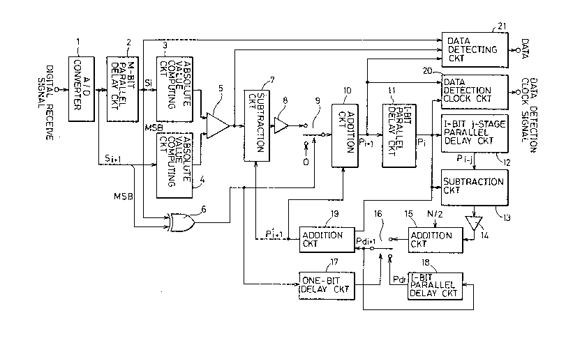
Fig. 1 is a block diagram showing one embodiment of
the present invention.
Fig. 2 is a diagram for use in comparing the result
obtained by data detection according to one embodiment of
the present invention with a background art method.
Fig. 3 is a diagram for use in explaining problems
arising in the use of the background art method.
Fig. 4 is a diagram showing a list of marks used in
the background art method and in the present invention.
DESCRIPTION OF THE PREFERRED EMBODIMENTS
Fig. 1 is a detailed block diagram of one embodiment
of the present invention. In the embodiment shown in Fig.
1, a description will now be made on the case where
-10-
digital data is detected from a digital receive signal
according to an NRZ type modulation system with a minimum
inversion space (Tmin) = 0.8T and a maximum inversion
space (Tmax) =-3. 2T . An A/D converter 1 is supplied with
a digital receive signal. This digital receive signal is
sampled at a frequency m times a channel bit rate by A/D
converter 1, and the sampled signal is then converted into
di~ital data of M bits. This conversion represents the
polarity of a reproduced signal by using, for example,
two's complement "0" and "1" of MSB (Most Significant
Bit).
An output of A/D converter 1 is first input to an M-
bit parallel delay circuit 2. M-bit parallel delay
circuit 2 has a delay amount cor~esponding to a sampling
period, whose output is applied as preceding sampling data
S1 to an absolute value computing circuit 3. An output of
A/D converter 1 is further applied as present sampling
data S~l to an absolute value computing circuit 4.
Respective outputs of absolute value computing circuits 3
and 4 are applied as absolute values ¦Si¦ and ¦Si+l¦ of
preceding and present sampling data to an arithmetic
circuit 5. Arithmetic circuit 5 ob'cains a phase interval
P between a present sampling point R1~l and a zero cross
point in accordance with the aforementioned expression (1)
by using the absolute values ¦Si¦ and ¦Si~ll of the
Cl~)
preceding and present sampling data. In order to
determine whether there is a zero cross point between the
present sampling point R1,l and the preceding sampling
point Ri, the MSs of outputs of A/D converter 1 and M-bit
parallel delay circuit 2 is input to an exclusive OR gate
(hereinafter referred to as the EXOR gate) 6. EXOR gate 6
outputs "1" when respective logics of two inputs are
different from each other. Since sampling data represents
a polarity by "1" or "0" of the MSB as described above, a
zero cross point exists between the present sampling point
and the preceding sampling point when an output of EXOR
gate 6 is "1".
An output of arithmetic circuit S is input to a
subtraction circuit 7. An output of an addition circuit
19 which i8 a predicted value P'l~l of the present phase is
input to the other input of substraction circuit 7 as will
be described later. Subtraction circuit 7 outputs the
result obtained by subtracting the output of addition
circuit 19 from the output of arithmetic circuit 5. An
output of subtraction circuit 7 is input to a coefficient
circuit 8. Coefficient circuit 8 multiplies the output of
subtraction circuit 7 by a certain coefficient K (0 < K <
1) and outputs the result of the multiplication.
Respective outputs of coefficient circuit 8 and EXOR gate
6 are input to a selecting circuit 9. As has been
-12-
~t~
described previously, since the phase interval P between
the present sampling point Ri~l and the zero cross point is
effective only when the zero cross point exists between
the present sampling point Ri+l and the preceding sampling
point R1, selecting circuit 9 selects the output of
coefficient circuit 8 when the output of EXOR gate 6 is
~ , i.e., the zero cross point exists between the present
sampling point R1+l and the preceding sampling point Ri,
while it outputs "0" when the output of EXOR gate 6 is
"0", i.e., there is no zero cross point between the
present sampling point R1,l and the preceding sampling
point Rl. The output of selecting circuit 9 is input to an
addition circuit 10. The output of addition circuit 19
which is the predicted value P'i,l of the present phase is
input to the other input of addition circuit 10 as will be
described later. Addition circuit 10 outputs the sum of
these two values, i.e., the present phase P1~l.
The output of addition circuit 10 which represents
the present phase Pl~l is input to an I-bit parallel delay
circuit 11. The I-bit parallel delay circuit 11 has a
delay amount corresponding to a sampling period, whose
output is input as a preceding phase P1 to an I-bit j-stage
parallel delay circuit 12 and a subtraction circuit 13.
I-bit j-stage parallel delay circuit 12 has a delay amount
of j times (j is a natural number) of a sampling period,
-13-
whose output is input as a phase P1j preceding by j+1 into
subtraction circuit 13. Subtraction circuit 13 subtracts
the output of I-bit j-stage parallel delay circuit 12 from
the output of I-bit parallel delay circuit 11, and outputs
the result obtained by subtracting a phase interval
between ideal sampling points from the result of the
subtraction of the output of I-bit j-stage parallel delay
circuit 12. The phase interval between ideal sampling
points is determined by the number j of stages of I-bit j-
stage parallel delay circuit 12. When j is odd, the phaseinterval is N/2, while when j is even, the phase interval
is zero. The output of subtraction circuit 13 is input to
a coefficient circuit 14. Coefficient circuit 14 outputs
the result obtained by multiplying the output of
subtraction circuit 13 by a certain coefficient L (0 < L <
1) ~
The output of coefficient circuit 14 is applied to an
addition circuit 15, so that a phase value N/2
representing a sampling period is added to the applied
output. An output of addition circuit 15 is input to a
selecting circuit 16. Selecting circuit 16 is also
provided with respective outputs of a one-bit delay
circuit 17 and an I-bit parallel delay circuit 18. One-
bit delay circuit 17 is provided with the output of EXOR
gate 6. This delay circuit 17 delays the output of EXOR
-14-
gate 6 by a time corresponding to the sampling period and
outputs the same. That is, the output of one-bit delay
circuit 17 indicates whether there is a zero cross point
between the preceding sampling point Ri and a sampling
point Ril which is two points preceding to the present
sampling point.
I-bit parallel delay circuit 18 is provided with an
output of selecting circuit 16. I-bit parallel delay
circuit 18 delays the output of selecting circuit 16 by a
time corresponding to the sampling period and outputs the
same. Selecting circuit 16 selects an output of addition
circuit 15 when the output of one-bit delay circuit 17 is
~ , i.e., a zero cross point exists between the preceding
sampling point Rl and the sampling point Ril which is two
points preceding to the present sampling point. When the
output of one-bit delay circuit 17 is ~lO~I, i.e., there is
no zero cross point between the preceding sampling point R
and the sampling point R~l two points before the present
sampling point, selecting circuit 16 selects the output of
I-bit parallel delay circuit 18 and outputs the selected
output as a predicted value Pdl~l of the phase interval
between the present sampling point Rl~l and the preceding
sampling point Ri. Accordingly, the output of I-bit
parallel delay circuit 18 is a predicted value Pdi of the
phase interval between the preceding sampling point Ri and
-15-
the further preceding sampling point Ril. The output of
selecting circuit 16 is input to addition circuit 19.
Addition circuit 19 has the other input provided with an
output of I-bit parallel delay circuit 11, i.e., a
preceding phase Pi. Addition circuit 19 calculates the sum
of these two values and outputs the result as a predicted
value P'i,~ of the present phase.
The foregoing phase calculation is not merely an
arithmetic operation but must be carried out in the range
of 0 to N - 1 similarly to, for example, a calculation of
angles made in the range of 0 to 360.
A data detection clock signal and digital data are
detected on the basis of the phase information thus
obtained. With reference to Fig; 1, a data detection
clock signal detecting circuit 20 is provided with an
output of addition circuit 10 which represents the present
phase P~,l and with an output of I-bit parallel delay
circuit 11 which represents the preceding phase. Data
detection clock signal detecting circuit 20 compares the
above-described clock signal extracting conditions and two
inputs. Then, if the conditions are satisfied, i.e.,
digital data at that time is effective, detecting circuit
20 outputs "1". On the other hand, if the conditions are
not satisfied, i.e., digital data at that time is
ineffective, detecting circuit 20 outputs l~0~. A
~.~r~
subsequent circuit, e.g., a demodulation circuit or the
like processes only effective digital data in response to
an output of data detection clock signal detecting circuit
20, i.e., a data detection clock signal.
Further, a data detecting circuit 21 is provided with
an MSB of an output of M-bit parallel delay circuit 2
which represents the polarity of the preceding sampling
data, an output of arithmetic circuit 5 which represents
the phase interval between the present sampling point Ri~l
and the zero cross point, and an output of I-bit parallel
delay circuit 11 which represents the preceding phase.
Data detecting circuit 21 compares the above-described
data determining conditions and those inputs, and detects
digital data in accordance with ~he respective conditions.
The present invention can be realized by the
foregoing method. The foregoing process will be organize~
as follows.
First, a determination is made as to whether a zero
cross point exists immediately before the present sampling
point Rl~l, i.e., between the present sampling point Ri+l and
the preceding sampling point Ri. If there is a zero cross
point, a phase interval P between the zero cross point and
the present sampling point R1~l is first obtained by the
following expression (9) by employing present sampling
data Si~l and its preceding sampling data S
-17-
P~.n
P = I Si+ll/(lSi+ll + I Si 1) x (N/2) --(9)
Next, a determination is made as to whether there is
any zero cross point immediately before a preceding
sampling point Ri, i.e., between the preceding sampling
point Rl and a sampling point Ril which is two poillts
before the present sampling point. If the zero cross
point exists therebetween, a predicted value Pdi+l of the
phase interval between the present sampling point Ri+l and
the preceding sampling point Ri is obtained by the
following expression (10) by employing a preceding phase P
and a phase Pl; of a sampling point which is two or more
points before the present sampling point.
Pdi+l = ~( Pi - Pij - (N/2 x ~) mod N) x L + N/2~ mod N
(L is a constant in the range of 0 < L ~ 1.) ...(10)
If the there is no zero cross point, the predicted
value Pdl+l of the phase interval between the present
sampling point Ri+l and the preceding sampling point Ri is
set to a predicted value Pdi of the phase interval between
the preceding sampling point Rl and the further preceding
sampling point Ril as shown in the following expression
(11) .
Pdl+l = Pdi ...(11)
A predicted value Pl+l' of the present phase is
obtained by the following expression (12) by employing the
-18-
s~
predicted value Pdi+~ of the phase interval thus obtained
and the preceding phase Pi.
P'i+l = (Pi + Pdi+~) mod N ...(12)
By use of the present phase predicted value P'i+~ thus
obtained and the phase interval P between the
aforementioned zero cross point and the present sampling
point Ri+l, the present phase Pi+l is obtained by the
following expression (13).
P1+l = { (P - P'i+~) x K + P'i+~} mod N (K is a constant
in the range of 0 < K < 1.) ...(13)
If there is no zero cross point immediately before
the present sampling point Ri+~, the present phase
predicted value P'1+l is set intactly to the present phase
P~
A data detection clock signal and digital data are
detected on the basis of the phase interval P between the
zero cross point and the present sampling point Ri+l, the
present phase P1+l and the preceding phase P1 thus obtained,
and the clock extracting conditions and the data
determining conditions. The clock signal extracting
conditions and the data determining conditions are shown
as follows which are the same as in the background art
method.
Pi > P1+~, Pi > N/2, and Pi~ > N/2: There is a clock signal.
Pi > P1+1, Pi < N/2, and PL+1 < N/2: There is a clock signal.
Pi ~ P1~l, Pl < N/2, and P1+l _ N/2: There is a clock signal.
When P > Pi+l - N/2, digital data is opposite to the
MSB of Si, or otherwise, the MSB of Si.
In the present invention, data errors due to
frequency variations of a receive signal, which is the
disadvantage of the background art method can be reduced
by using the above-described method, and a higher
reliability of the system can be retained.
Like the case with the background art method, such a
case is now considered that the receive signal shown in
Fig. 3 (b) is sampled at a double channel bit rate and
then input to the data detector of one embodiment of the
present invention. First, a phase interval P between a
zero cross point and the present sampling point is
obtained in accordance with sampling data. Like the
foregoing background art method, since this method is
effective only with respect to sampling points Rl and R8,
the phase interval P in each case is as follows.
Sampling point Rl: P = ¦ Sl ¦/(¦S~¦ + ¦S0l) x N/2 =
30/(30 + 23) x 32 = 18
Sampling point Rs: P = ¦ S8 ¦ /( ¦ S31 + ¦ S7 ¦ ) X N/2 = 5/
(5 + 47) x 32 = 3
Next, a predicted value PdL+l of the phase interval
between the present sampling point Ri+~ and the preceding
-20-
sampling point R1 is obtained. In the case with a sampling
point R~, since there is no zero cross point between its
preceding sampling point Ro and a sampling point Rll which
is two points before the sampling point Rl, a predicted
value Pdl of the phase interval is a predicted value Pdo=
32 of the phase interval between the preceding sampling
point Ro and the further preceding sampling point Ri~ as
shown in the above expression (11). If a predicted value
Pl' of the present phase is obtained by using this
predicted value, the result is as follows by the above
expression (12).
Pl' = PO + Pdl = 24 + 32 = 56
If the present phase Pl is obtained from the above
result and from the previously obtained P, the result is
as follows by the above expression (13).
Pl = { (P - Pl') x K + P~'} mod N = {(18 - 56) x 0.25
+ 56} mod 64 = 62
Next, in the case with a sampling point R2, since
there is a zero cross point between its preceding sampling
point Rl and a sampling point Ro which is two points before
the sampling point R2, a predicted value Pd2 of the phase
interval is as follows by the above expression (10) where
j = 2.
Pd2 = {(Pl - Pl) xL + N/2} mod N = ~(62 -56) x 0.25 +
-21-
32} mod 64 = 33
If a predicted value P2' of the present phase is
obtained from the above result, the predicted value is as
follows by the expression (12).
P2' = (Pl ~ Pd2) mod N = (62 + 33) mod 64 = 31
In this case, since there is no zero cross point
between the present sampling point R2 and the preceding
sampling point Rl, the present phase P2 is the predicted
value P2' of the present phase. With respect also to
sampling points R3 - R9, if P, Pdi+l, P'i+l and Pi+l are
obtained, the results are as shown in Fig. 2 (d) - (g).
If a data detection clock signal and digital data are
generated on the basis of the clock signal extracting
conditions and the data determining conditions by use of
the results shown in Fig. 2 (d) - (g), results are as
shown in Fig. 2 (h) and (i). These results match
transmitted data. Thus, the use of the method of the
present invention makes it possible to detect accurate
digital data from the receive signal having frequency
variations and data errors which occur in the background
art method.
While the foregoing description has been made on the
case where an input is one channel, the present invention
is also applicable to the case where an input is a multi-
channel. In the case with Y channels, for example, a
-22-
Z.,~
receive signal of each channel is sampled at a different
timing, and each delay time of M-bit parallel delay
circuit 2, I-bit parallel delay circuits 11 and 18, one-
bit parallel delay circuit 17 and I-bit j-stage parallel
delay circuit 12 is multiplied by Y.
While the foregoing embodiment has been directed to
the NRZI type modulation system with Tmin = 0.8T and Tmax
= 3.2T, the present invention is not limited to this and
also applicable to other modulation systems.
As has been described heretofore, in accordance with
the present invention, it is possible to provide a digital
data detector which can handle a digital receive signal
having larger frequency variations than that of background
art, by obtaining a predicted value of a phase interval
between the present sampling point and its preceding
sampling point from a phase of the preceding sampling
point, a phase of a sampling point which is two or more
points preceding to the present sampling point, and the
position of a point at which the digital receive signal
crosses a reference signal, and then obtaining a phase of
the present sampling point from the obtained predicted
value.
Although the present invention has been described and
illustrated in detail, it is clearly understood that the
same is by way of illustration and example only and is not
-23-
n
to be taken by way of limitation, the spirit and scope of
the present invention being limited only by the terms of
the appended claims.
-24-