Note: Descriptions are shown in the official language in which they were submitted.
WO 92/00502 PCTlUS91/04194
-1-
DEMODULATION REFERENCE SIGNAL SOURCE
BACKGROUND OF THE INVENTION
The present invention concerns demodulators
for phase modulated signals and, more particularly,
demodulators for phase modulated signals obtained from
electromagnetic waves subjected to phase modulation.
Fiber optic gyroscopes are an attractive means
with which to sense rotation of an object supporting
such a gyroscope. Such gyroscopes can be made quite
small and can still be constructed to withstand
considerable mechanical shock, temperature change, and
other environmental extremes. In the absence of moving
parts, they can be nearly maintenance free, and they
have the potential of becoming economical in cost. They
can also be sensitive to low rotation rates that can be
a problem in other kinds of optical gyroscopes.
Such fiber optic gyroscopes have a coil of
optical f fiber wound on a core and about the axis thereof
around which rotation is to be sensed. The optical
ffiber is typically of a length of 100 to 2,000 meters,
or so, and is part of a closed optical path in which an
electromagnetic wave, or light wave, is introduced and
split into a pair of such waves to propagate in opposite
directions through the coil to both ultimately impinge
on a photodetector. Rotation about the sensing axis of
the core, or the coiled optical ffiber, provides an
effective optical path length increase in one rotational
direction and an optical path length decrease in the
other rotational direction for one of these waves. The
opposite result occurs for rotation in the other
direction. Such path length differences between the
waves introduce a phase shift between these waves for
either rotation direction, i.e. the well known Sagnac
i ~
WO 92/00502 PCT/US91/04194
-2-
2~g~1~2
effect. The use of a coiled optical fiber is desirable
because the amount of phase difference shift due to
rotation, and so the output signal, depends on the
length of the entire optical path through the coil
traversed by the two opposing direction electromagnetic
waves, and so a large phase difference shift can be
obtained in the long optical fiber but in a relatively
small volume taken by it through being coiled.
The output current from the photodetector
system photodiode, in response to the opposite direction
traveling electromagnetic waves impinging thereon after
passing through the coiled optical fiber, follows a
raised cosine function. That is, the output current
depends on the cosine of the phase difference between
these two waves. Since a cosine function is an even
function, such an output function gives no indication as
to the relative directions of the phase difference
shift, and so no indication as to the direction of
rotation about the coil axis. In addition, the rate of
change of a cosine function near zero phase is very
small, and so such an output function provides very low
sensitivity for low rotation rates.
Because of these unsatisfactory
characteristics, the phase difference between the two
opposite direction traveling electromagnetic waves is
usually modulated by placing an optical phase modulator
on one side of the coiled optical fiber. As a result,
one of the opposite direction propagating waves passes
through the modulator on the way into the coil while the
other wave, traversing the coil in the opposite
direction, passes through the modulator upon exiting the
coil.
.,.
CA 02085122 2000-06-02
' 64159-1218
3
In addition, a phase-sensitive detector serving as
part of a demodulator system is provided to receive a signal
representing the photodetector output current. Both the
optical phase modulator and the phase-sensitive detector can be
operated by a sinusoidal signal generator at the so-called
"proper" frequency to reduce or eliminate modulator induced
amplitude modulation, but other waveform types of the same
fundamental frequency can be used. Other frequencies can also
be used, and often are to reduce the frequency level to a more
manageable value.
The resulting signal output of the phase-sensitive
detector follows a sine function, i.e. the output signal
depends on the sine of the phase difference between the two
electromagnetic waves impinging on the photodiode, primarily
the phase shift due to rotation about the axis of the coil in
the absence of occurrence of other significant but unwanted
phase shifts. A sine function is an odd function having its
maximum rate of change at zero phase shift, and so changes
algebraic sign on either side of zero phase shift. Hence, the
phase-sensitive detector signal can provide an indication of
which direction a rotation is occurring about the axis of the
coil, and can provide the maximum rate of change of signal
value as a function of rotation rate near a zero rotation rate,
i.e. the detector has its maximum sensitivity for phase shifts
near zero so that its output signal is quite sensitive to low
rotation rates. This is possible, of course, only if phase
shifts due to other sources, that is, errors, are sufficiently
small. In addition, this output signal in these circumstances
is very close to being linear at relatively low rotation rates.
Such
WO 92/00502 PCT/US91/04194
-4-
2 p-g-512 2
characteristics for the output signal of the
phase-sensitive detector are a substantial improvement
over the characteristics of the output current of the
photodetector.
An example of such a system from the prior art ';~;
is shown in Figure 1. The optical portion of the system
contains several features along the optical paths to
assure that this system is reciprocal, i.e. that
substantially identical optical paths occur for each of
l0 the opposite direction propagating electromagnetic waves
except for the specific introductions of non-reciprocal
phase difference shifts, as will be described below.
The coiled optical fiber forms a coil, 10, about a core
or spool using a single mode optical fiber wrapped about
the axis around which rotation is to be sensed. The use
of a single mode fiber allows the paths of the
electromagnetic or light waves to be defined uniquely,
and further allows the phase fronts of such a guided
wave to also be defined uniquely. This greatly aids
maintaining reciprocity as well as the introduction of
non-reciprocal phase shifts as is indicated to be done
below.
In addition, the optical fiber can be
so-called polarization-maintaining fiber in that a very
significant birefringence is constructed in the fiber so
that polarization fluctuations introduced by unavoidable
mechanical stresses, by the Faraday effect in magnetic
fields, or from other sources, which could lead to
varying phase difference shifts between the counter-
propagating waves, become relatively insignificant.
Thus, either the high refractive index axis, i.e. the
slower propagation axis, or the low index axis is chosen
for propagating the electromagnetic waves depending on
WO 92/00502 PGT/US91/04194
-5- 208122
the other optical components in the system. In the
present system, the slow axis has been chosen in view of
the optical components used therein.
The electromagnetic waves which propagate in
opposite directions through coil 10 are provided from an
electromagnetic wave source, or light source, il, in
Figure 1. This source is typically a laser diode which
provides electromagnetic waves, typically in the near
infrared part of the spectrum, with a typical wavelength
of 830 nm. Source 11 must have a short coherence length
for emitted light to reduce the phase shift difference
errors between these waves due to Rayleigh and Fresnel
scattering at scattering sites in coil 10. Because of
the nonlinear Kerr effect in coil 10, different
intensities in the two counter propagating waves can
lead to different phase shifts therebetween.. This
situation can be overcome also by use of a short
coherence length source for source il which leads to
modal phase shift canceling.
Between laser diode 11 and fiber optic coil 10
there is shown an optical path arrangement in Figure 1
formed by the extension of the ends of the optical fiber
forming coil 10 to some optical coupling components
which separate the overall optical path into several
optical path portions. A portion of the same kind of
polarization-maintaining optical fiber as in coil 10 is
positioned against laser diode 11 at a point of optimum
light emission therefrom, a point from which it extends
to a first optical directional coupler, 12.
Optical directional coupler 12 has light
transmission media therein which extend between four
ports, two on each end of that media, and which are
shown on each end of coupler 12 in Figure 1. One of
WO 92/00502 PCT/US91/04194
.z~8~~~2
-6-
these ports has the optical fiber extending from laser
diode il positioned thereagainst. At the other port on
the sense end of the optical directional coupler 12
there is shown a further optical fiber positioned
thereagainst which extends to be positioned against a
photodiode, 13, which is electrically connected to a
photodetection system, 14.
' Photodiode 13 detects electromagnetic waves,
or light waves, impinging thereon from the portion of
the optical fiber positioned thereagainst and provides
a photo current in response. This photocurrent, as
indicated above, in the case of two nearly coherent
light waves impinging thereon, follows a cosine function
in providing a photocurrent output which depends on the
cosine of the phase difference between such a pair of
substantially coherent light waves. This photovoltaic
device will operate into a very low impedance to provide
the photo current which is a linear function of the
impinging radiation, and may typically be a p-i-n
photodiode.
Optical directional coupler 12 has another
optical fiber against a port at the other end thereof
which extends to a polarizer, 15. At the other port on
that same side of coupler 12 there is a non-reflective
termination arrangement, 16, involving another portion
of an optical fiber.
Optical directional coupler 12, in receiving
electromagnetic waves, or light, at any port thereof,
transmits such light so that approximately half thereof
appears at each of the two ports of coupler 12 on the
end thereof opposite that end having the incoming port.
On the other hand, no light is transmitted to the port
..
WO 92/00502 PCT/US91/04194
28.5122
_7_
which is on the same end of coupler 12 as is the
incoming light port.
Polarizes 15 is used because, even in a single
spatial mode fiber, two polarization modes are possible
in light passing through the fiber. Thus, polarizes 15
is provided for the purpose of passing one of these
polarization modes through the optical fiber, along the
slow axis thereof as indicated above, while blocking the
other. Polarizes 15, however, does not entirely block
light in the one state of polarization that it is
intended to block. Again, this leads to a small non-
reciprocity between two opposite direction traveling
electromagnetic waves passing therethrough and so a
small non-reciprocal phase shift difference occurs
between them which can vary with the conditions of the
environment in which the polarizes is placed. In this
regard, the high birefringence in the optical fiber used
again aids in reducing this resulting phase difference,
as indicated above.
Polarizes 15 has a port on either end thereof
with the light transmission medium contained therein
positioned therebetween. Positioned against the port on
the end thereof opposite that connected to optical
directional coupler 12 is another optical fiber portion
which extends to a further optical bidirectional
coupler, 17, which has the same light transmission
properties as does coupler 12.
The port on the same end of coupler 17 from
which a port is coupled to polarizes 15 again is
connected to a non-reflective termination arrangement,
18, using a further optical fiber portion. Considering
the ports on the other end of coupler 17, one is
connected to further optical components in the optical
i ~ a
WO 92/00502 PCT/US91/04194
~0~~~-2~
_8_
path portions extending thereto from one end of the
optical fiber in coil 10. The other port in coupler 17
is directly coupled to the remaining end of optical
fiber 10. Between coil 10 and coupler 17, on the side
of coil 10 opposite the directly connected side thereof ,
is provided an optical phase modulator, 19. Optical
phase modulator 19 has two ports on either end of the
transmission media contained therein shown on the
opposite ends thereof in Figure 1. The optical fiber
from coil 10 is positioned against a port of modulator
19. The optical fiber extending from coupler 17 is
positioned against the other port of modulator 19.
Optical modulator 19 is capable of receiving
electrical signals to cause it to introduce a phase
difference in light transmitted therethrough by changing
the index of refraction of the transmission medium, or
transmission media, therein to thereby change the
optical path length. Such electrical signals are
supplied to modulator 19 by a bias modulation signal
generator, 20, providing a sinusoidal voltage output
signal at a modulation frequency fg that is equal to
Clsin(ogt) where ~g is the radian frequency equivalent
of the modulation frequency fg. Other suitable periodic
waveforms could alternatively be used.
This completes the description of the optical
portion of the system of Figure 1 formed along the
optical path followed by the electromagnetic waves, or
light waves, emitted by source 11. Such electromagnetic
waves are coupled from that source through the optical
fiber portion to optical directional coupler 12. Some
of that light entering coupler 12 from source 11 is lost
in non-reflecting terminating arrangement 16 coupled to
a port on the opposite end thereof , but the rest of that
r i
WO 92/00502 PGT/US91/04194
._. 2085122
-g-
light is transmitted through polarizes 15 to optical
directional coupler 17.
Coupler 17 serves as a beam-splitting
apparatus in which the light entering the port thereof,
received from polarizes 15, splits approximately in half
with one portion thereof passing out of each of the two
ports on the opposite ends thereof. Out of one port on
the opposite end of coupler 17 an electromagnetic wave
passes through optical fiber coil 10, modulator 19, and
back to coupler 17. There, a portion of this returning
light is lost in non-ref lective arrangement 18 connected
to the other port on the polarizes 15 connection end of
coupler 17, but the rest of that light passes through
the other port of coupler 17 to polarizes 15 and to
coupler 12 where a portion of it is transmitted to
photodiode 13. The other part of the light passed from
polarizes 15 to coil 10 leaves the other port on the
coil 10 end of coupler 17, passes through modulator 19,
and optical fiber coil 10 to re-enter coupler 17 and,
again, with a portion thereof following the same path as
the other portion to finally impinge on photodiode 13.
As indicated above, photodiode 13 provides an
output photocurrent, IPD13' pr°portional to the
intensity of the two electromagnetic or light waves
impinging thereon' and is therefore expected to follow
the cosine of the phase difference between these two
waves impinging on that diode as given by the following
equation:
I
Ip~~- 2 (1+cos (~R+~pmcosc~9t) l
i ~ a
WO 92/00502 PCT/US91/04194
-10-
This is because the current depends on the resulting
optical intensity of the two substantially coherent
waves incident on photodiode 13 , an intensity which will
vary from a peak value of Io to a smaller value
depending on how much constructive or destructive
interference occurs between the two waves. This
interference of waves will change with rotation of the
coiled optical fiber forming coil 10 about its axis as
such rotation introduces a phase difference shift of ~
between the waves. Further, there is an additional
variable phase shift introduced in this photodiode
output current by modulator 19 with a maximum value of
and which varies as cos(~gt).
Optical phase modulator 19 is of the kind
described above and is used in conjunction with a
phase-sensitive detector as part of a demodulation
system for converting the output signal of
photodetection system 14, following a cosine function as
indicated above, to a signal following a sine function.
Following such a~sine function provides in that output
signal, as indicated above, information both as to the
rate of rotation and the direction of that rotation
about the axis of coil 10.
Thus, the output signal from photodetection
system 14, including photodiode 13, is provided through
an amplifier, 21, where it is amplified and passed
through a filter, 22, to such a phase sensitive detector
means, 23. Phase-sensitive detector 23, serving as part
of a phase demodulation system, is a well known device.
Such a phase-sensitive detector senses a change in the
first harmonic, or fundamental frequency, of modulation
signal generator 20 to provide an indication of the
relative phase of the electromagnetic waves impinging on
i r i
WO 92/00502 PCT/US91/04194
208~I2~
-11-
photodiode 13. This information is provided by
phase-sensitive detector 23 in an output signal
following a sine function, that is, this output signal
follows the sine of the phase difference between the two
electromagnetic waves impinging on photodiode 13.
Bias modulator signal generator 20, in
modulating the light in the optical path at the
frequency fg described above, also generates harmonic
components in photodetection system 14. Filter 22 is a
band-pass filter which is to pass the modulation
frequency component of the output signal of
photodetector 14, i.e. the first harmonic, after its
amplification by amplifier 21.
In operation, the phase difference changes in
the two opposite direction propagating electromagnetic
waves passing through coil 10 in the optical path,
because of rotation, will vary relatively slowly
compared with the phase difference changes due to
modulator 19. Any phase differences due to rotation, or
the Sagnac effect, will merely shift the phase
differences between the two electromagnetic waves. The
amplitude scaling factor of the modulation frequency
component of the output signal of photodetection system
14, appearing at the output of filter 22, is expected to
be set by the sine of this phase difference modified
further only by the factors of a) the fixed magnitude of
the maximum phase modulation value of these waves due to
modulator 19 and generator 20, and b) a constant
representing the various gains through the system.
Then, the periodic effects of this sinusoidal modulation
due to generator 20 and modulator 19 in this signal
component are expected to be removed by demodulation in
the system containing phase-sensitive detector 23
WO 92/00502 PCT/US91/04194
-12-
leaving a demodulator system (detector) output signal
depending on just the amplitude scaling factor thereof.
However, these desired results may not be
achieved in the system of Figure 1. The output of
amplifier 21 will provide a voltage output signal based
not only on the in-phase photocurrent generated in
photodiode 13 in photodetector system 14, as indicated
by the first equation above, but also on a quadrature
component of that photocurrent not given by that
equation. Such a quadrature component usually arises in
the optical system portion of Figure 1, typically due to
intensity modulation induced by phase modulator 19.
There can be other sources for such a quadrature
component such as due to "pick-up" from other signals
present in the system.
Furthermore, there will be added phase delay
beyond that which is shown in the first equation above.
Some of this phase shift will be introduced in
photodetection system 14, and that phase shift will be
both temperature dependent and component aging dependent
so that its value at any time during operation will
typically not be known, and will vary in subsequent
operation. There are other sources of such phase shift
also, including the phase shift across modulator 19
between the phase of the signal supplied by generator 20
and the response of modulator 19 in having the index of
refraction of the media therein, or its length,
correspondingly change. Thus, the output signal of
amplifier 21 will have a phase delay therein with
respect to the phase of the signal provided by generator
20. This additional phase, 9, is equivalent to a time
delay of duration Td where tJTD=8 if the phase shift is
i r I
WO 92/00502 PCT/US91/04194
2085122
-13-
linear with frequency or a reasonable approximation can
be made that is linear.
Thus, the voltage at the output of amplifier
21 will typically appear as:
Vz1-out - k{1+cos tax+~Dcos (~~t+8) ] ) + a sin (c.~9t+8)
with the left-hand term being based on the in-phase
component of the photodiode output current and the
right-hand sine term being based on the quadrature
component of that voltage at the modulation frequency.
The constants k and E represent the gains through the
system to the output of amplifier 21. The other symbols
used in the preceding equation have the same meaning
they did in the first equation above. The foregoing
equation can be expanded in a Bessel series expansion to
give the following:
Vas-o~c - a sin (~~t + 8)
+ k C 1 + Jo ( Vim) cos ~R]
- 2kJ1 (gym) sin ~pRCOS (~~t+8)
- 2kJ2(tpm)coscpRcos2(c~~t+8)
+ 2kJ3 (rpm) sin~Rcos3 (c~9t+8)
WO 92/00502 PCT/US91/04194
14
+ ~ [(-1)n2kJ2n(cp,~) coscpRCOS2n(c~t + 8)
n-2
+ (-1)n2kJ2n+i (cp~,) sincpRcos (2n+1) (cyt + 8)]
This signal at the output of amplifier 21 is applied to
the input of filter 22.
Filter 22, as indicated above, passes
primarily the first harmonic from the last equation,
i.e. the modulation frequency component. As a result,
the output signal of filter 22 can be written as
follows:
V22-out ' -2kJ1 (~m) sin(~R cos ( W9t+B+llfl) +E8ln (cast+B+14f1)
The further phase delay term appearing, ~1, is the
additional phase shift in the first harmonic term added
as a result of passing through filter 22. This added
phase shift is expected to be substantially constant and
a known characteristic of filter 22.
The signal from filter 22 is then applied to
phase-sensitive detector 23, as is the signal from bias
modulation generator 20, the latter again being equal to
Clsin(c~gt) where ~g is the radian frequency equivalent
of the modulation frequency fg. Since the value of the
added phase shift girl in filter 22 is known, a phase
shift equal to that can be added by phase-sensitive
detector 23 before using that signal. However, the
phase shift B is unknown, and so cannot be added by
phase-sensitive detector 23. The output of
WO 92/00502 PCT/US91/04194
2085122
-15-
phase-sensitive detector 23, based on the known behavior
of such devices, will then be the following:
v23-out ' k~J~ ~~pD~ cos9sin~pR + k~ k sin6
The constant k' accounts for the gain through
phase-sensitive detector 23. As can be seen, a cosine
factor depending on B appears in the in-phase component
based portion of the output signal of phase-sensitive
detector 23. The added phase shift B will affect the
accuracy of the portion of the output of phase-sensitive
detector 23 represented by the term in which cosh
appears. In addition, a significant quadrature
component based portion of this output signal having a
sine factor depending on 8 will also be present at the
output signal of phase-sensitive detector 23, and will
often constitute a significant error in being much
larger than the in-phase component based portion which
can be relatively small at low rotation rates. Thus,
there is desired a demodulation arrangement which will
avoid the presence of this quadrature related term in
the output signal of the phase-sensitive detector.
SUMMARY OF THE INVENTION
The present invention provides an information
retrieval system for extracting information from a pair
of substantially coherent electromagnetic waves from a
source, with such information being represented by phase
differences therebetween, each of which waves is
incident on a photodetector. These waves have further
phase differences therebetween varying at a modulation
frequency due to being phase modulated with the
photodetector being capable of providing an output
CA 02085122 2000-06-02
' ' 64159-1218
16
signal representing the waves as incident thereon but also
representing any further processing phase shifts arising
because of the generation of the waves or due to the
photodetector. The information retrieval system comprises a
demodulator which receives the photodetector output signal and
also receives a reference signal. The reference signal is
obtained though use of a phase shift detector which receives
the photodetector output signal, and which determines at least
the processing phase shift occurring therein, providing this
information to a reference signal supply to adjust the phase of
its output signal, along with predetermined phase shift
information previously provided thereto, which is supplied as a
reference signal to the demodulator. The forgoing
electromagnetic waves are developed in the source thereof as
opposite direction traveling waves through a fiber optic coil
and modulated by an optical modulator in the optical path of
these waves. The first harmonic of the photodetector signal is
primarily supplied to the demodulator, with the phase shift
detector receiving a selected one of (a) the time integral of
the photodetector signal, (b) the time derivative of the
photodetector signal, and (c) the second harmonic component of
the photodetector signal.
In accordance with the present invention, there is
provided an information retrieval system for extracting
information from a pair of substantially coherent
electromagnetic waves represented by phase differences
therebetween each of which is incident on a photodetector
means, said pair of substantially coherent electromagnetic
waves being provided by a source generation means with further
phase differences provided therebetween varying at a modulation
frequency due to each being phase modulated, said photodetector
means being capable of providing an output signal at an output
thereof representing said pair of substantially coherent
CA 02085122 2000-06-02
' ' 64159-1218
16a
electromagnetic waves as incident thereon and also representing
any further processing phase shifts, said information retrieval
system comprising: a demodulator means having an information
signal input electrically connected to said photodetector means
output, and having a reference signal input and an output, said
demodulator means being capable of providing at said output
thereof an output signal substantially free of frequency
components at said modulation frequency corresponding to an
input signal provided at said information signal input thereof
having a substantial signal component therein at said
modulation frequency if a reference signal at said modulation
frequency having a selected phase relationship with said input
signal modulation frequency component is provided at said
reference signal input thereof; a phase shift detection means
having an input electrically connected to said photodetector
means output, and having an output, said phase shift detection
means being capable of providing at said output thereof an
output signal containing a representation of that said
processing phase shift occurring in input signals provided at
said information signal input of said demodulator means at said
modulation frequency; and a reference signal supply means
having an input electrically connected to said phase shift
detection means output, and having an output electrically
connected to said demodulator means reference signal input,
said reference signal supply means being capable of providing
at said output thereof an output signal with a phase determined
by both input signals provided at said input thereof and by
predetermined phase shift information previously supplied
thereto.
BRIEF DESCRIPTION OF THE DRAWINGS
Figure 1 shows a mixed block and circuit schematic
diagram of a system known in the prior art,
CA 02085122 2000-06-02
64159-1218
16b
Figure 2 shows a mixed block and circuit schematic
diagram embodying the present invention which can be
substituted for a portion of the diagram of Figure 1,
Figure 3 shows a mixed block and circuit schematic
diagram embodying the present invention which
WO 92/00502 PGT/US91/04194
205122
_1~_
can be substituted for a portion of the diagram of
Figure 1, and
Figure 4 shows a mixed block and circuit
schematic diagram embodying the present invention which
can be substituted for a portion of the diagram of
Figure 1.
DETAILED DESCRIPTION OF THE PREFERRED EI~ODIMENTS
Because the added processing phase shift 8
generated in the optical portion of Figure 1, and in
photodetection circuit 14 thereof, varies with
temperature and time, there is no satisfactory way of
predicting its value. Yet, elimination of a quadrature
term in the output of phase-sensitive detector 23 can be
accomplished only through demodulating the rotation rate
data signal supplied thereto from filter 22 by use of a
reference signal which is synchronized and phase matched
(in-phase) with this rotation rate data signal. Since
this cannot be the situation for the reference signal
supplied by bias modulation generator 20, as that signal
is not subject to the sources of phase shift affecting
the output signal of filter 22, the output signal of
that generator cannot be the direct source of the
reference signal used in phase-sensitive detector 23 as
shown in Figure 1. Rather, the reference signal for
phase-sensitive detector 23 must be obtained from the
rotation rate data signal since that is the only signal
which has in it the information as to the value of the
added processing phase shift 8 due to the optical system
and photodetection system 14.
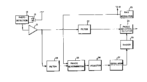
Hence, the lower portion of Figure 1, after
amplifier 21 and before phase-sensitive detector 23,
must be modified to permit extracting a suitable
reference signal from the rotation rate data signal
WO 92/00502 PCT/US91/04194
-18-
~0~512~
supplied at the output of filter 22. One manner of
accomplishing this is shown in the system of Figure 2
which can be substituted for the portions of the system
of Figure 1 not directly involved in the optical portion
of that system. The system and circuit components of
Figure 2 which are the same as those shown in Figure 1
carry the same numerical designations in each figure.
As indicated above, the output of amplifier 21
is a signal voltage that is based on the photocurrent
developed through photodiode 13 because of the
impingement of the two electromagnetic waves thereon
from the optical system portion shown in Figure 1. This
output voltage, v21_out, comprises a portion based on the
quadrature component of the photodiode current, and a
portion based on the harmonic components plus a constant
polarity term forming the in-phase component of the
photodiode current as shown in the equation above for
the expanded version of this voltage. Again, filter 22
selects primarily the harmonic component of the in-phase
portion of v2i-out at the modulation frequency fg, i.e.
the first harmonic thereof, and presents that as its
output voltage, v22-out ~ to the data input of
phase-sensitive detector 23.
This voltage signal at the output of filter
22, as the equation therefor above shows, contains the
added processing phase shift 8 of unknown but changing
value. This phase shift value must be added as an
additional phase shift in the reference signal to be
supplied at the reference signal input of
phase-sensitive detector 23, as well as adding other
known phase shifts thereto, if demodulation of a
sufficient quality is to be provided to eliminate any
.,. ~ r
WO 92/00502 PGT/US91/04194
2085122
-19-
quadrature component from the voltage signal developed
at the output of phase-sensitive detector 23.
In Figure 2, the source of that information as
to the value of 8 is obtained from the second harmonic
of the in-phase component of the photodiode output
current as represented in the voltage signal at the
output of amplifier 21 in the manner indicated by the
above equation for v21-out (although a higher order even
harmonic could have been chosen). This is accomplished
through a further bandpass filter, 24, having its input
connected to the output of amplifier 21. The pass band
of filter 24 is centered about the frequency of the
component of the output voltage of amplifier 21
representing the second harmonic of the output current
of photodiode 13, and so provides the following voltage
signal at the output of filter 24:
yaa-oat ' -2kJ2 (gym) Cos~RCOB C2 (ca9t+8) +1~f21
The added phase shift ~r2 in f filter 24 beyond that at the
output of amplifier 21 is the phase shift contributed by
filter 24.
Output voltage v24-out of filter 24 is provided
to a phase determination means, 25. Phase determination
means 25 is typically a zero-crossing detector to detect
the zero-crossings of output voltage v24-out that occur
closest to the zero-crossings of the output voltage of
bias modulation generator 20. Since the processing
phase shift 9 added by the optical system of Figure 1
and photodetection system 14 thereof is expected to be
relatively small, the zero-crossings of second harmonic
filter 24 output voltage v24-out that are of interest
will be those relatively close to the zero-crossings of
WO 92/00502 PCT/US91/04194
208512
-20-
bias modulation generator 20. The zero-crossings of
interest of the second harmonic component of the output
of amplifier 21 provided by filter 24, that is, the
output voltage v24-out of filter 24 , can be seen to be
from the foregoing equation to occur at
n 8
- 2W9 (2n-1) 2 - ~g - 2w9
These follow from the cosine time dependence of output
voltage v24-out and the argument thereof as shown in the
equation preceding the last. These zero-crossing points
serve as synchronizing time values in operating a
subsequent oscillator.
These synchronizing values from phase
determination means 25 are provided to a phase adjuster,
26. Phase adjuster 26 is provided to remove any
differences in the phase delays introduced in filters 22
and 24, and can do so since such phase delays in each
are stable and predictable. This difference is equal to
$2/24~g-~1/~lg.
Phase adjuster 26 adds this difference in time
delay to the synchronizing values supplied thereto and
then passes them on to an oscillator, 27. This
oscillator generates a corresponding oscillatory output
which can be a cosine wave or, often more conveniently,
a square wave. The output of oscillator 27 at the
second harmonic frequency 2fg is supplied to a divider,
28, which divides the frequency by 2 to provide an
oscillatory output wave having corresponding modulation
frequency zero-crossings, or zero-crossings at
_,.. ~ r
WO 92/00502 PGT/US91/04194
208512
-21-
(2n-1)
9
These are exactly in phase with voltage v22-out supplied
at the output of filter 22, and thus an accurate
demodulation is supplied of this latter voltage by
phase-sensitive detector 23. As a result, the output of
phase-sensitive detector 23 will be
Vzs-ouc ' k~Ji <<Pm) sin ~x
where k' again represents the accumulated gain constants
in the system. If the amplitude of the phase modulation
provided by bias modulation generator 20 and
modulator 19 stays constant, then v23-out will depend
only on the sine of the rotation induced phase
difference ~
Alternatively, oscillator 27 could be
eliminated if phase determination means 25 provides, as
an output signal therefrom, an oscillatory signal with
zero-crossings occurring exactly at the synchronizing
values described above. Then, adjuster 26 would adjust
the phase of this oscillatory wave from phase
determination means 25, and the resulting oscillatory
signal at the output of adjuster 26 would be divided by
divider 28. As a result, oscillator 27 is shown with a
dashed line therethrough to indicate the alternative of
eliminating that component. In this latter approach,
divider 28 and adjuster 26 could be interchanged in
position with oscillator 27 eliminated.
As an alternative which eliminates having to
filter the higher frequency involved in making use of
the second harmonic component of the output voltage
WO 92/00502 PCT/US91/04194
-22-
signal of amplifier 21, that output signal can instead
be integrated after removing the constant polarity term
therefrom. Such a system is shown in Figure 3. The
constant polarity term is removed by a capacitor, 30,
with the remaining portions of the output voltage of
amplifier 21 then supplied to the input of an
integrator, 31. The result of the integration over time
that provides a corresponding voltage at the output of
integrator 31 can be written in expanded form as
v3~-ouc ' - w kJl (cps) sincpRSin (cast+8)
9
- 1 kJ2 (cps,) coscpRSin2 (w9t+8)
2wg
+ 1 kJ3 (cpm) sin~Rsin3 (w9t+8)
3w9
+~ [(-1)° 1 kJZn(~~)coscpRsin2n(w9t+B)
n_Z 2nw9
+ (-1)n 1 kJZn,l (cPm) sin~Rsin(2n+1) (wgt+8) ]
(2n+1 ) w9
where the integral of the quadrature term has been
neglected. Although the quadrature term in the output
voltage of amplifier 21 can be significant with respect
to the in-phase term at low rotation rates, the
quadrature term will always be very small with respect
i
WO 92/00502 PCT/US91/04194
2Q85122
-23-
to the second harmonic component of the output voltage
of that amplifier.
The time integration performed by integrator
31 can be seen in the last equation to convert all of
the time dependencies of the harmonic components in the
output signal of amplifier 21 to being time dependent
only through sine functions. Differing from cosine
functions, the sine functions of the harmonics have
amplitudes that cross zero value at various times but
to all cross zero value at the same time the amplitude of
the first harmonic, or fundamental (at the modulation
frequency f9), crosses zero. Thus, a zero-crossing
detector can be used again for phase determination means
25 to select those zero-crossings of the output voltage
of amplifier 21 which are close to the zero-crossings of
the output voltage of bias modulator generator 20. The
zero-crossings of the output voltage of integrator 31
will be
na _ 8
n
~Q
As a result, the remaining portions of Figure 3 can for
the most part match those of the system of Figure 2
including phase determination means 25, phase adjuster
26 and an oscillator 27. However, a divider is omitted
as the zero-crossings in the system of Figure 3 are
determined commensurate with the fundamental or first
harmonic component of the output voltage of amplifier 21
rather than its second harmonic component as in the
system of Figure 2. Again, oscillator 27 can be
omitted, as indicated by the dashed line therethrough,
in circumstances where phase determination means 25
WO 92/00502 PGT/US91/04194
°zo8~~~~
-24-
provides an oscillatory output rather than merely
providing synchronizing pulses indicating zero-crossings
of the output voltage of integrator 31. Phase adjuster
26 is then adjusted to provide a phase delay equal to
that provided by band-pass filter 22, or girl.
However, if the harmonic components of the
output voltage of amplifier 21 are not equally well
integrated by integrator 31 because of bandwidth
limitations therein, for instance, some of the higher
and more poorly integrated harmonics will no longer
cross zero amplitude value at the same time that the
fundamental harmonic does. Hence, the bandwidth of
integrator 31 must be sufficient to integrate all of the
harmonic components of the output voltage of amplifier
21 which have any significant amplitude. As an
alternative, a differentiator, 31' , shown as a dashed
line box in Figure 2, could be substituted for capacitor
30 and integrator 31 to provide a time dependence in the
harmonics that is again represented in a set of harmonic
sine functions. This may, in some circumstances, be a
more desirable choice than integration.
The systems of Figures 2 and 3 both require
forming a reference signal for phase-sensitive detector
23 therein which has a frequency equal to that in the
output voltage of bias modulation generator 20, or
modulation frequency fg, a frequency which might
typically be on the order of 50 kHz. Phase-sensitive
detection, or demodulation, that requires shifting from
a frequency at the fundamental of the rotation rate data
signal supplied at the output of filter 22, i.e. fg, to
a baseband frequency value devoid of any significant
amount of the modulation frequency, or the harmonics
thereof, can be difficult to do accurately because of
i r ,
WO 92/00502 PCT/US91/04194
20851~~
-25-
limitations in the components available for phase-
sensitive detector 23. Figure 4 shows an alternative
approach, based on the example of the system of Figure
3, which uses two steps in the demodulation of the
output signal vz2_out of filter 22. In the first step,
the frequency of the modulation frequency component, or
fundamental component, of voltage v22-out ~ supplied by
amplifier 21 and selected by filter 22, is first shifted
to a much lower frequency, a typical value being 3 kHz.
The resulting signal at that frequency is then submitted
to a phase-sensitive detector to complete the
demodulation process, that detector also receiving a
reference signal at this lower frequency for that
purpose.
To provide such a two step demodulation, the
system of Figure 3 is shown modified in Figure 4 as an
example, and includes modifying bias modulation
generator 20 thereby leading to its being redesignated
20' in Figure 4. Generator 20' now has three different
output voltages which have a fixed frequency and phase
relationship with one another such as can be established
through using phase-lock techniques in a well-known
manner. The modulation output voltage of generator 20'
is, of course, supplied as it was in the system of
Figure 3 remaining equal to Clsinegt. This voltage
waveform at modulation frequency fg is again supplied to
modulator 19, and is again supplied to phase
determination means 25. Thus, the zero-crossings of the
output voltage of integrator 31 which are closest to the
zero-crossings of the generator 25 output voltage
waveform operating modulator 19 can again be found just
as they were in the system of Figure 3. Generator 20'
further supplies a frequency shifting voltage output
WO 92/00502 PGT/US91/04194
~zo~~m~
-26-
waveform C2cosine(c~et+ag) which might have a frequency
value for ~8/2n = fg of 47 kHz if fg = 50 kHz. There
will be some phase shift associated therewith also which
has been designated as. This voltage is applied to a
frequency down converter, 23', as part of the
demodulation system to provide a downward shift in the
effective modulation frequency so that the output signal
from down converter 23' will have frequencies around 3
kHz. This voltage C2cosine(~gt+ae) from generator 20'
is mixed with the rotation rate data signal supplied at
the output of filter 22, or v22-out as given above. This
mixing will result in the following voltage signal at
the output of frequency down converter 23'
v23~-out - klJ1 (~m) sin~RCOS [ (W9-(J8) t+B+t~fl - aeJ
+ eosin [ (c~9-c~8) t+8+~rl-a8]
There is typically no difficulty with a system component
frequency shifting or converting like frequency down
converter 23' in being capable of providing a frequency
conversion at the frequency levels involved therein, 47
kHz and 50 kHz. Demodulation difficulties of the kind
indicated above arise instead in going from the
modulation frequency directly to the baseband. The
constants k' and E' represent the cumulative effect of
system component gain constants occurring through the
system to the point of the output of frequency down
converter 23'.
Generator 20' provides a third output signal
C3cosine(odt+ad), and supplies it to the phase adjuster
which merely supplies a phase change therein before
.,. ~ t
WO 92/00502 PGT/US91/04194
2085122
-27-
passing it on, and so has been redesignated 26' in
Figure 4. The frequency ed/2n = fd is fixed at being
the difference between the other two frequencies
supplied thereby, fg and fs or ed = 41q-cus. This can be
seen to be precisely the frequency occurring in the time
dependent terms in the equation for the output voltage
v23~-out of frequency down converter 23' above. Hence,
the equation for the output voltage of frequency down
converter 23' can be rewritten
V23~-out ' -k~J~ (cpm) sin~Rcos (cads+8+~rl-ag)
+ eosin ( cadt+8+~rl+aa)
Thus, this output voltage signal from
frequency down converter 23' can be clearly demodulated
so as to eliminate the quadrature based term therein by
a cosine waveform varying with radian frequency cad, and
just such a voltage is available from bias modulation
generator 20' as indicated above, voltage
C3cosine(c~dt+ad). However, a phase shift must be added
thereto so that it has the same phase as the in-phase
cosine term in the preceding equation. Hence, this
voltage from generator 20' to be supplied to adjuster
26' must have a phase adjustment made thereto equal to
8+il-as-ad. As indicated above, phase shifts (a) ~l,
due to filter 22, (b) ag, appearing in the frequency
shifting signal supplied from bias modulation generator
20' to frequency down converter 23', and (c) ad,
appearing in the demodulation signal supplied from bias
modulation generator 20' to adjuster 26' are all known,
and so can be preset in adjuster 26'. Phase shift B,
WO 92/00502 PCT/US91/04194
~zo$~~.22
-28-
due to the optical system and photodetection circuit 14,
is not fixed and known, but its values are obtained from
phase determination means 25. These are found from the
zero-crossing times of the bias modulation generator
20' , which occur at tn = n~r/~g, and the zero-crossing
times of the signal from integrator 31, which are
tn = (nn-9)/~g, as clearly these equations permit B to
be determined. Thus, adjuster 26' has the information
necessary to provide the proper additional phase shift
to the demodulation signal being supplied by bias
modulation generator 20' to provide an output signal
from adjuster 26' as follows:
V26~-out ' C3cos ( c~dt+8+~r-a9)
This output signal from adjuster 26' supplies the
reference signal for phase-sensitive detector 23 " and
will be accurately synchronized with the output signal
of down converter 23' for demodulating the rotation data
rate signal supplied to detector 23 " thereby. The
result will be
V23~~-out ' kllJ1 ( ~m) 8 in~R
where again no quadrature based component results. The
constant k " again represents the accumulated component
gain constants through the system.
Although the present invention has been
described with reference to preferred embodiments,
workers skilled in the art will recognize that changes
may be made in form and detail without departing from
the spirit and scope of the invention.
." i r