Note: Descriptions are shown in the official language in which they were submitted.
W O 9l/20l72 2 ~ 3 2 PCT/GB91/01008
Resonant Inverter
This invention relates to inverters.
More particularly, the invention relates to inverters of the kind
comprising a resonant circuit including a capacitor and an inductor, a
first main switching device arranged to conduct current from a d.c.
source in one direction through the capacitor and inductor, a second - -
main switching device arranged to conduct current from the d.c. source
through the capacitor and inductor in the opposite direction, and drive
means for causing the switching devices to conduct alternately, the
drive means comprising a tranformer having a primary winding in series
with the capacitor and inductor and two secondary windings arranged to
provide drive signa~s to the respective main switching devices.
An inverter of this kind is described in published European patent
application EP-A-O 121 917. The described inverter opera~es at the
resonant frequency of the resonant circuit, the main switching devices
being switched at the zero crossing points of the oscillatory current in -
the resonant circuit, and there is no means of controlling the power
output of the inverter.
A paper by Sebastian et al, entitled "Regulating Self-Oscillating
Resonant Converters", 2nd European Conference on Power Electronics and
Applications held at Grenoble, France, on 22-24 September 1987 describes
an inverter in which switching of the field-effect transistors forming
the main switching devices is effected by two saturable transformers
with primaries connected in the resonant circuit and secondaries
connected to the gates of the field-effect transistors, so that the
SV~;TIT~ITE ~;~IEET
. . . . - . . ~ .. .. . - . . ..
... ~ . , , , ~. . . ... . . .
. . . `. . -. . .
.. .~ . ., . ~.. - . . , . : , , , :
. . ~ , . . . . . .
: ~. - .. . . ~ ~ - . .. . . ` ..
W O 91/20172 2 ~ PCT/GB91/01008
- 2 -
drive to each transistor is removed when the associated transformer
saturates. Each transformer has an additional winding through which a
variable controlled d.c. current is fed, to control the point at which
the transformer saturates. The switching of the transistors can thereby
be controlled to control the phase difference between the voltage and
current in the resonant circuit so as to control the power output of the
inverter. However, the described inverter is relatively complex.
It is an object of this invention to provide an improved inverter.
In accordance with this invention, an inverter of the kind set
' forth is provided with control means for controlling the s~itching of
the main switching devices, the control means comprising means for
sensing reversal of current in the resonant circuit after one of the
main switching devices has been turned on, means for turning off the
switching device a predetermined time after current reversal, and means
for varying the predetermined time.
Preferably, the means for sensing reve~sal of current comprises an
additioral transformer having a primary winding connected in the
resonant circuit and a secondary winding connected to timing means
operable to provide a signal for turning off the main switching device
after the predetermined time.
In one form of the invention, the means for turning off the main
switching device comprises a secondary switching device connected across
the associated secondary winding of the drive transformer so as to
remove the drive from the main switching device when the secondary
switching device is turned on by the signal from the timlng means.
Sl,lBSTlTUTE SHEET
..... . . . . .. . .
.~: . . . . . . .. .. . . ., .... . . ~ ,.... .. .. ..
- .. . . . . . . .
., ` . . . . . ` ~ .
~, .. , . . . .. . . . .. .. ... .- . ~ ..
.,.. ~ .. ` ,, . , ,. . .. , . .. . . ,.; : `
W O 91~20172 2 ~ ~ ~1 3 2 PCT/CB91/01008
Preferably, the drive transformer has a core of magnetisable
material with a square hysteresis loop characteristic, so that following
turning off of the said main switching device a predetermined time after
current reversal, the other main switching device is turned off by
saturation of the drive transformer after a period of time from the next
current reversal equal to the said predetermined time.
In one form of the invention, the first and second main switching
devices are connected in series across the d.c. source, two capacitors
are connected in series across the d.c. source, and the capacitor and
inductor of the resonant circuit are connected in series between the
junction of the said two capacitors and the junction of the main
switching devices. -
In another form of the invention, the first and second main
switching devices are connected in series across the d.c. source, and
third and fourth main switching devices are connected across the d.c.
source to form a bridge circuit with the first and second main switching
devices, the capacitor and inductor of the resonant circuit being
connected in series between the junction of the first and second main
switching devices and the junction of the third and fourth main
switching devices, and the drive transformer has additional secondary
windings arranged to provide drive signals to the third and fourth main
switching devices respectively so that the main switching devices in
opposite arms of the bridge circuit are turned on simultaneously.
The inverter may be used-to supply a load connected across the
SUE3STlTlDTE 5HEET
W O 91/20172 ~ 3, 13 ~ PCT/GB91/01008
inductor or the capacitor of a resonant circuit. As described in more
detail below, the circuit is a form of "Boucherot circuit", a
characteristic of which is that the load current is independent of the
load. As eY~plained below, this gives the inverter of the present
invention advantages, particularly when the inverter is connected to an
a.c. mains supply and is used to supply a load at constant potential,
for example a battery being charged, in that the current is taken from
the mains supply at or close to unity power factor and with little or no
harmonic content.
The invention will now be described, by way of example, with
reference to the accompanying drawings, in which:
Figure 1 is a circuit diagram of an inverter in accordance with
this in~ention,
Figure 2 is a diagram of a control circuit of the inverter,
Figure 3 and 4 illustrate alternative loads which can be supplied
by the inverter, and
Figure 5 is a circuit diagram of a modified form of the inverter of
this invention. ~`
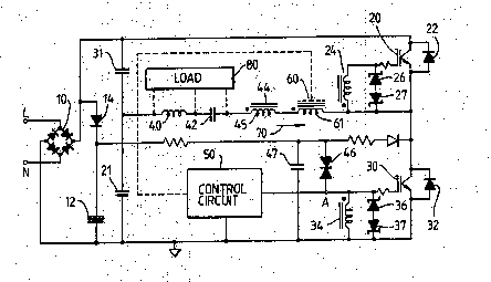
Referring to Figure 1, the resonant inverter circuit is connected
to a d.c. supply, provided by a full-wave rectifier 10, connected for
examp}e to the mains supply. A smoothing capacitor }2 is connected in
series with a diode 14 across the d.c. supply.
The power circuit of the inverter comprises a bridge of two
transistor switches 20 and 30 connected in series across the d.c. supply
and two capacitors 21 and 31 also connected in series across the d.c.
SUBSTITUTE~ SHEET
.~., . . . . .. , . : .
`.` . .. ` . ` . . .,, . , . . . ' ` . "; . . .. . ., ~ i . .
W ~ 9t/20172 2 ~ ~ ~ 1 3 r~ PCT/GB91/01008
supply, and an inductor 40 and capacitor 42 connected in series be~ween
the junction of transistors 20 and 30 and the junction of capacitors 21
and 31. Diodes 22 and 32 are connected across transistors 20 and 30. `
The load 8O is connected to inductor 40 or capacitor 42, as described
below with reference to Figures 3 and 4.
A drive circuit to ePfect switching of the transistors 20 and 30
consists of a drive transformer 44 having a prima~y winding 46 in series
with the inductor 40 and capacitor 42 and two secondary windings 24 and
34 connected to the gates of transistors 20 and 30 respectively. Zener
diodes 26 and 27 are connected across the secondary 24 to limit the
voltage applied to transistor 20. Zener diodes 36 and 37 are similarly
connected across secondary 34. Drive transformer 44 has a magnetisable
core with a square hysteresis loop characteristic.
To initiate oscillation, a starting circuit is provided, consisting
of a diac 46 connected between the positive line of the d.c. supply and
the gate of transistor 3O, and a capacitor 47 connected across the diac
46 and the secondary 34 of drive transformer 44. :
To control the conduction ~imes of the transistor switches 20 and
3O~ a control circuit 5O is provided, which will now be described with
reference to Figure 2. A field-effect transistor 51 is connected in
series with a diode 52 across the secondary winding 34 of drive
transformer 44, so that when transistor 51 is conducting, the drive is
removed from transistor switch 3O. Transistor 51 is controlled by means
of an integrated circuit timer 52 of the well-known type "555". The
SUBSTlTlJTE SHE~ET
~ , ~
W O 91/20t72 2 ~ ~ tj l ~i ~ PCT/GB91/01008
characteristics of the timer 52 are such that the output at pin 3, is ;
low when the voltages at the trigger pin 2 and the reset pin 4 are low.
When the voltages at the trigger pin 2 and reset pin 4 go high, the
output at pin 3 goes high, and remains high for a preset period, after
which it reverts to the low value. The preset period is determined by
the time constant of a potentiometer 53 and capacitor 54 connected to
pins 6 and 7 of the ti~er 52 and to 12 volt supply 55, derived from the
d.c. supply. The output of the timer 52 at pin 3 is applied to the gate
of transistor 51 through transistors 56 and 57, which are also connected
to the 12-volt supply, so that transistor 51 is turned on when the
oùtput at pin 3 is high.
The voltages applied to the trigger pin 2 and reset pin 4 of the
timer 52 are derived from a current transformer 60, the primary winding
61 of which is connected in series with inductor 40 and capacitor 42, so
as to sense the oscillatory current in the resonant circuit. Zener
diodes 63 and 64 are connected across the secondary winding 62 of
transformer 60, so that output of the transformer 60 appears as a square
wave. The output is supplied to the emitter of a transistor 66, the
base of which is connected to ground and the collector of which is
connected to the reset pin 4 of the timer 52 and through resistor 65 to j-
the 12-volt supply, so that when the output of the transformer current
60 is positive transistor 64 is non-conducting and the voltage at reset
pin 4 is high. The output of the transformer 60 is also supplied to the `
base of transistor 66 so that when the output is positive transistor 68 -
,'`" '.
-;~; .
SUE~STITUTE SHIFET
~ . .
W 0 91/20172 2 ~ PC~/GB91/01008
is conducting and transistor 67 is held non-conducting so that the
potential of the 12-volt supply is applied to the trigger pin 2 of timer
52 through resistor 69. When the output voltage of the current
transformer 60 is negative, the voltages applied to the reset pin 4 and
trigger pin 2 of the timer 52 are low.
In operation of the circuit, the main transistor 20 and 30 conduct
alternately. Suppose that transistor 30 is conducting. Current flows
in the direction shown by arrow 70 from the d.c. supply through
capacitor 31, inductor 40, capacitor 42, the primaries 45 and 61 of
transformers 44 and 60, and transistor 30. Transistor 30 is held
conducting until the drive provided by the voltage across the secondary `
winding 34 of the drive transformer 44 falls to zero. Ignoring for the
moment the operation of the control circuit 50, this occurs on
satùration of the drive transformer 44, or when the current falls to ;
zero, if this occurs before saturation. On switching off of transistor
30, the current (if it has not reached zero) is diverted through diode
22 until it falls to zero. The current in the resonant circuit will
then reverse, flowing initially through capacitor 21 and diode 32. '~
Reversal of the current through the primary 45 of drive transformer 44
generates a voltage across the secondary 24 which switches on transistor
switch 20, so that current flows from the d.c. source through switch 20
and capacitor 21. Transistor 20 remains on until the transformer 44
saturates (or the oscillatory current falls to zero). When transistor
20 switches off, current flows through diode 32 until it falls to zero
.:
SUBSTITIJTE SHEET ~ :
:
, ;, ` :. , . ,. ~. ~ .. :
W O 91/20172 ~ ~ ~ 5 1 ~ 2 PCT/GB91/01008
- 8 -
and reverses, flowing initially through diode 22, until the voltage
across secondary 34 of drive transformer 44 turns on transistor 3C
agaln .
Operation of the inverter, in the absence of the control circuit
5O, would thus be similar to that of the prior art inverter referred to
above. If the transistor 20 and 3O tùrn off when the oscillatory ;~ ~:
current falls to zero, the inverter will operate at its resonant
frequency, with the output voltage developed across inductor 40 and
capacitor 42 in phase with the oscillatory current. If the transistor -
:,: ~. .
20 and 3O are turned off before the oscillatory current reaches zero,
the output voltage is out of phase with the oscillatory current so that
the power output of the inverter is reduced. ~ -
In accordance with the present invention, the control circuit 50
operates to turn off transistor switch 30 after a time determined by the
setting of the potentiometer 53. The circuit operates as follows.
When, in each cycle, the oscillatory current begins to flow in the
direction shown by arrow 70 in Figure l, the voltage generated across ~ ;
the secondary 62 of current transformer 60 causes the potentials at the
reset pin 4 and trigger pin 2 of the timer 52 to go high, so that the
timer is initiated and the output at pin 3 goes high, holding transistor
51 non-conducting. The transistor switch 3O is therefore turned on by
drive transformer 44,~as described above. At the end of the period
determined by the potentiometer 53 and capacitor 54 the output pin 3 ; `~
goes low, and transistor 51 is turned on. The drive to the gate of
SUBSTITIJTE S~EET
~ . ` '
W O ~1/20172 2 ~ Pcr/GBsl/o1on8
- 9 -
transistor 30 is therefore removed and transistor 30 becomes
non-conducting. The current flowing through inductor 40 and capacitor
42 is then diverted through diode 22 and flows through the circuit
including diode 22 and capacitor 31, until the current falls to zero and
begins to reverse, whereùpon transistor 20 is turned on by the action of
drive transformer 44. Since the core of trans~or~er 44 has a "square
loop" characteristic, it cannot sustain an output voltage integral in
one sense greater than the other, and the core saturates, removing the
drive from transistor 20, a~ter a period, measured from current
reversal, equal to the predetermined period (when the current is flowing
in the opposite direction) after which transistor 30 is turned off by .
timer 52. After transistor 20 is turned off, the current flows through
the circuit including diode 32 and capacitor 21 until it reverses, ~ ,
whereup transistor 30 is turned on by drive transformer 44, timer 52 is ;
triggered by current transformer 60, and the cycle commences.
The power output of the inverter can thus be controlled by varying .
the setting of potentiometer 53. .
The inverter can be used to supply various loads. Figure 3 shows
an example in which the inverter provides power for an induction hob 82.
The inductor 40 is incorporated into the hob 82 so that the base of a
ferrous metal pan ô4 placed on the hob in close proximity to the
inductor will be heated by-induced high frequency eddy currents and
hysteresis losses, to cook the pan contents.
Figure 4 illustrates a more conventional load 90, connected to the
SUBSTITUTE~ StlEE~T
........ . .. .. . ............... . . . . . .
. . ~ . . .. ~
W O 91/20172 2 a ~ ~ PCT/GB91/01008
- 10~ "
capacitGr 42 through an isolating transformer 86 and a rectifier 88.
The load could, for example, be a rechargable battery or Dagnetron.
Figure 5 shows a modified form of the inverter. The circuit is the
same as that shown in Figures 1 and 2, except that the capacitors 21 and
31 of the Figure 1 circuit have been replaced by two additional
transistor switches 120 and 130. The drive transformer 44 has two '~
additional secondary windings 124 and 134 connected to the gates of the
additional transistors 120 and 130. Voltage-limiting zener diodes 126,
127 and 136, 137 are connected across the secondaries 124 and 134, and
diodes 122 and 132 are connected across transistors lZ0 and 130.
Secondary windings 124 and 134 are wound so that transistor 120 is
turned on simultaneously with transistor 20 and transistor 130 is turned
on simultaneously with transistor 30. Transistors 120 and 130 turn off
when the drive transformer 44 saturates or the current through its
primary winding 45 falls to zero. The control circuit 50 operates in :
the same way as in the embodiment of Figures 1 and 2.
The embodiment of Figure 5 effectively provides a full bridge
configuration as compared to the half-bridge configuration of Figure 1. `~
The voltage applied to the series resonant circui~ in the embodiment of
Figure 5 is equal to the full supply voltage, rather than half the
supply voltage in the Figure 1 embodiment. The value of the oscillatory `~
current is therefore reduced by half for the same output power. The
embodiment of Figure 5 thus has an advantage when operating at high
power levels.
; ~'`'`"'
:
`SUBSTITUTE~ SHET
"'~.
.. ` ` . . . ~ ~ .. . ` .... . . ... . , .,. .; . -j ` .,
W O 91/20172 2 ~ PCT/GB9t/01008
The circuits shown in Figures 1 and 4, in which the load is
connected across the capacitor or inductor of a resonant circuit, are
circuits of the kind known as a "Boucherot circuit". A characteristic
of such a circuit is that the load current is independent of the ioad.
In general, when such a circuit is operating at its resonant fequency'~
the load current I is given by: ~.
I = V
~3L
where V is the voltage applied across the resonant circuit and L is the
inductance of the circuit. ..
In the case of the circuit shown in Figure 1, the effect of the
control circuit 50 is to modify the Boucherot constant, so that the load
current is given by:
I = V . cos
~ . ~:
where ~ is the phase angle between the resonant current and the
switching sequence of transistor switches 20 and 30. The control
circuit 50 operates to vary ~ between 0 , at which the load current is ~
maximum, and 90, at which the load current is reduced to zero, ~ :
If the circuit is connected to an A.C. mains supply through a
full-wave rectifier as shown in Figure 1, the voltage across the
resonant circuit, since capacitors 21 and 31 are small, is an unsmoothed
rectified waveform whose amplitude is a rectified sinusoid of mains
~ '';' ' ,:
SlJBSTITUTE~ SHEFT
;.. .- .. . , . ,. ~.` . . .. .- - . -.. . . - . :
W O 91/20172 2 ~ l 3 ~ PCTtGB91/01008
- 12 -
frequency. The output load current may therefore be expressed as:
I = Vsin~. cos
~ L
where Vsin~ is the instantaneous value of the supply potential.
The power supplied to the load is given by:
` ' .
load- I VlOad. Vsina. cos
where VlOad is the voltage across the load-
If the circuit is used to supply, for example, a battery being
charged via a transformer rectifier, or a capacitor resistive load being -`
charged to a constant potential, the voltage VlOad is constant, and
the load power is proportional to Vsin~, ie. to the instantaneous value
of the mains supply voltage, The current drawn from the mains supply
must there~ore be a square wave of unity power factor and phase.
The described circuit thus has advantages over conventi al battery
charger circuits or capacative input filters which take non-unity power
factor currents with a harmonic content tending to contravene ;`
.:
regulations relating to the harmonic content of mains supply current.
The circuit of Figure 4 as the same advantages. ~ ~
-:
,~
SUBSTlTlJTE SHE~ET
.. . `, . . .. , ` .- ` . . ~