Note: Descriptions are shown in the official language in which they were submitted.
SPECIFICATION
Title of the ~vention
METHOD ~OR PAll~RNING A LAY~R O~ OXIDE
SUPERCO~DU(: TOR THIN ~LM AND
SIJPERCONDUClING DEVICE MANUFACrURED
- THEREBY
Background of the ~vention
1 0 Field o~ ~e invention
'rhe present invention re~ates to a me~hod ~o~ patteming a layer on
a~ oxide supercondurtor thin ~ilm and a superconducting device
manu~actured by ~he method, and mo~e specifically to a method for
patterning a layer on an oxide superconductor ~in ~i]m wi~out degrading
~he o~ide superconductor thin film, and a superconducting device
manufactured by ~he method.
Description o~ related art
Devices which u~ e super~onducting phenomena operate rapidly
2 0 with low power consumption so that they have higher perfo~nance t~an
conventional semiconductor devices. Particularly, by usin~ an oxide
superconductitlg mate~al which has ~en ~ecently ~dvanced in s~udy, it is
possible to produce a superconducting device which ope~tes at relatively
high temperature.
Joseph~on deviçe is one of well hlown superco~duc~ing devices.
Howe~er, since Josephson device is a two-te~ninal device, a logie ga~e
l- ~51~9
2~
which utilize~ Josephson devices becomes complicated, Ther~îore,
~ee-te~ninal super~onducting devices are more practical.
Typical three~terrninal superconduct~ng devices ~nclude two types
super-FET (field effec~ transistor). The first ~ype of the super-~l~T
S ~cludes a semiconductor channel, and a superconduc~r source electrode
and a superconductor drai~ elec~rode which are formed closely to each
other on both side of the semi~onductor chalmel. A po~ion of the
semiconductor layer between the superconductor sour~e electrode and ~e
superconductor d~ain electrode has a greatly ~eces~çd or undereut rear
10 sur~ace so as to hav~ a reduced thickness. In addition, a ga~e electrode is
fo~ned ~rough a gate insulating layer on the por~ion of ~e recessed or
undercut rear surface of the semiconductor layer between ~he
supercondalctor sollrce ~lect~ode and the superconductor drain electrode.
A superconducting current f1QWS through the sem;conductor layer
15 (channel) between the superconductor source eIectrode and the
superconductor d~ain elec~rode due ~o a supe~conducting proximity effect,
and is eontrolled by ~n applied ga~e voltage. This type of ~e super-FET
operates at a higher speed with ~ low power consumption.
l~e second type of the super-FET includes ~ chanDel of a
20 supe~onductor folmed between a sol~rce electrode and a drain electrode,
so ~hat a cur~ent flowing through the superconducting channel is
controlled by a voltage applied to a gate formed above the
superconducting channe].
Both of the super-l~ETs men~ioned a~ove are voi~age contsolled
2 5 devices which are eapable of isolating output signal ~rom anput ol~e and of
having a well de~med gain.
~5~g
2~J~3~r~
However, since ~he first type of the super FET utilizes the
superconducting proximity ef~ect, the superconductor source electrode
and the supercotlductor drain electrode have to be positioned within a
distance of a ~ew times the coherencc leng~h of the superconductor
materials ~f ~e superconductor source electrode and the superconduc~or
drain electr~de. Tn par~icular, since an oxide superconductor has a short
coherence length, a distance be~ween the supercvnductor source electrode
and ~e superconductor drain electr~de has ~o be made ]ess than about a
~ew ten nanometers, i~ the superconductor source electrode and tl~e
10 superconductor drain electrode a~e formed of the oxide superconduc~or
material. However, it is very di~lc~lt to conduct a fine processing such
as a fine patte~n etc~ing, so as to satisfy the very short separa~ion distance
mentioned above.
On the other hal~d, the super-FET having the superconducting
15 channel has a large cur~ent capability, and the fine processill~ which is
required to produc~ the ~irst type of the super-FEl' is not neec1ed to
prod~ct t~is type of super-FET.
In order ~ obtaîn a complete ON/OFP operation, both of the
superconducting channel and the gate insulating layer should have an
20 extremely thin ~icknes~. Por example, ~he supercorldl~cting charmel
formed of an oxide superconduc~r material should have a t~ickness of
less than five nanome~ers and ~he gate insulating layer should have a
thickness more than ten nanometers which is suf~icient ~o pr~vent a tunnel
currellt.
2 5 In ~e super-FET, since the extremely thin superconducting channgl
is ~onnested to ~he relatively thick supe~orlduc~ing sour~e regi~n and the
super~onducting dMin region at ~eir lower pOl'tiORS, the superconduct~ng
3 1515~
,
. .
2~ g
current flows substantially horizontally through the superconducting
channel and substantially vertically in the supercorlducting sollrce region
and ~e ~uperconductillg drain regioll. Since dle oxide superconduc~or h~
dle ~argest critical current density Jc in the direction perpendicular to
5 c-axes of its crystal lattices, the superconducting chamlel is pre~erably
formed of a c-axis oriented oxide superconductor thin film and the
superconducting source region and ~he superconducting drain region are
preferably formed of a a~is oliented oxide supereonduc~or ~in films.
In a prior art, in order to manufacture the super-FET which has ~e
1 o superconducti~g channel of c-axis oriented oxide superconductor thin ~
and ~e superconducting source region and the superconducting drain
region of a-ax;s oriented oxide superconductor thin films, a c-axis
oriented oxide superconductor thin film is ~o~ned at first and the c-axis
oriented oxide superconductor thin film i3 etched and removed excluding
15 a portion which will be the superconducting channel. Then, an a-axis
oriented oxide superconductor thin film is deposited so as to form the
supe~condue~ing source region and the superconducting drain region.
In another prior art, at first an a-axis oriented oxide
superconductor thin ~ilm is deposi~ed and etched so as to ~orm ~he
2 0 superconducting source region and the superconducting drai~ region, and
~ell a c-axis oriented oxide superconductor thin ~ilm is deposited so as to
fonn the superconducting ehalmel.
In t~e above rnethods, the oxide superconductor th;n ~llrn is mostly
processed by pho~oli~ography. Namely, the oxide supercollductor ~hin
2 5 ~llm is masked by a photoresist and etched by a we~ etchillg proeess using
a weak H3PO4 sollltion, or a dry e~ching process sueh as a reactive iOIl
etching or an ion-milling using Ar ions. ~ ord~r ~o process the oxide
~ 4 - 161~
,
2~$~cÇ~9
superconductor thm film without degradation, the oxide superconduc~or
thin film should be prevented ~rom contacting with water. Since the
oxide superconductor has high reac~ivity so as to react with water and i~
degraded. Ther~fore~ ~ese etchi~g process use little water.
S However, an oxide superconductor also reacts wi~h photoresist
remover so that a ~urface of the oxide superconductor thin ~IIm on which
a photoresis~ is fionned and removed is roughened. It is ve~y di~ficult to
deposit ano~er thin film or layer on the rough su~ace of the oxide
superconductor thin ~ilm so as to manu~acture a supercondueting device
or a superconducting circuit of a multi-layer structure. In addition, if
ano~er oxide superconductor thin ~ilm is formed so as to contact the
rough sur~ace, an undesirable Josephson junc~ion or a resistance is
~enerated al the inte2face. Purthermore, superconducting characteristics
of the reac~ed o~ide superconductor thin film is af~ected, so that she
superconducting device does not have an enough performal~ce.
Summary of ~e ~vention
Accordingly, it is an object of the present invention to provide a
method for patterning a layer on an ox;de superconductor thin film,
20 which have overcome the above mentioned de~ects of the collventiondl
ones.
Ano~er object of the present invention is ~o provide a me~hod ~or
processing an oxide superconductor thin film, which have overcome the
above mentioned defects of ~he conventional ones.
2 5 Still another object o~ dle present inv~ntion is ~o p~wide a med~od
~or mamlfacturing an FET type superconduc~ing device which have
overcome ~e above mentioned de~cts of the comrentiQnal ones.
'
- 5 - 151S~
5~JI9
Ano~er o~.ject o~ the preseIlt invention is to prov;de a~ PET type
superconductillg device having a superconduc~ g region ~o~stitu~ed of an
extremely thin oxide superconductor ~lm, which have overcome t~e
above men~ioned de~ects of the conventional olles.
The above and other objects of ~e present invention are achieved ~n
accordance wi~ the presen~ invention by a method ~or patteming a layer
whicl) is folmed on an oxids superconductor thin film characteri~ed in
that a weak H~ solution, a buffer solution including HF or a mixture
including HF is used for etching the layer.
Preferably, the HF concentration of the weak HF solution, the
buffer solution including H~ or the mixture including HP is S to 15 wt%.
An oxide superconductors is nst a~fected by this weak ~F solu~ion so that
the exposed portion of the oxide supercondllctor thin film is not
roughened.
Ac~ording to another aspect of the present invention, there is
provided a method for pat~erning an oxide superconductor thin film,
comprising a step OI forming a SiO2 layer on the oxide superconductor
thin film, patterning the SiO2 layer so as to fo~n the same pattern ~s tha~
of the oxide superconductor thin film whicb will be pat~e~ed, etching ~e
oxide superconductor thin film by using the pa~terned sio2 1ayer as a
mas~, and removing the sio2 layer by using A weak HF solu~on, a bl2ffer
solution including HF or a mixture including HP.
In ~is mcdlod, ~e HF concentration of the weak HF solution, the
bufIer solution including HF or the mixture including HF is preferably S
2 5 ~o 15 wt%. This weak HP solu~ion sel~ctively etches SiO29 ~herefore, ~e
~xide superconductor thin ~llm is not a~fected.
15159
- . - . -
In one preferred embodin~ent, the SiO2 layer is also patte~ed by
using a weak HP solution, a bu~er solution including HP or ~ mixture
including HP.
According to stilI another aspect of th~ present invention, there is
s proYided a method of manufacturing a superconducting device,
comprising the steps of forming on a principal surface of a sub~trate a
non-superconducting o~ide layer ha~ing a similar c~stal structure to that
of a c axis oriented oxide superconductor thin film, folming a c-axis
oriented ox~de superconductor thin film haYing an extremely thin
I O ~hickness on the non-superconducting oxide layer, ~o~ning an insulatillg
layer on the c-axis oriented oxide superconductor thin ~llm, ~olming a
gate electrode of polycrystaIline silicon on a cen~er portion of the
insulating layer, etching th~ insulatihg layer by using the gate electrode so
as to folm a ga~e insulati~g layer under the gate electrode and ~ITning an
15 a-axis oriented o~ide superconductor ~hin ~lm so as to embed the gate
elec~r~de and ~o îo~n an insulating region by dif~used silicon from the
gate electrode, and et~hing back the ~axis oriented oxide superconductor
thin film so that all upper surface of the a~axis oriented oxide
superconductor ~in ~ilm is planarized and the gate electrode is exposed at
2 0 the planarized upper su~ace of the a-axis oriented oxide superconductor
thin film and a superconducting source region and a superconducting
drain region are fonned at ~e both sides of the gate eIectrode.
It is pr~ferable th~t the insulating layer is ~tched by using a weak
HP solution, a bu~fer solution including HP or a mixture including HP.
25 this case, the superconducting channel of the extremely thin c-axis
oriellted oxide superconductor f;lm is not a~fected by tlhe ~ching process.
The~fore, the superconducting device h~s ~ high per~o~ance.
- 7 - ~5
,
: .
,9
According to further another aspect of the present invention, there
is provided a superconducting device compris~ng a substrate having a
principal surface, a non-super~onducting oxide l~yer h~ving ~ similar
crystal structure to that of the o~Eide superconductor, an extremely thin
S superconducting channel formed of a c~axis oriented oxide
xuperconductor thin film on the non-superconducting oxide layer, a
superconducting source region and a superconducting drain region
fonned of an a-axis oriented oxide superconductor thin ~ilm at the both
sides of the superconduc~ing channe} separated from each o~er, which are
electrically comlected each other by the superconducting channel, so that
superconducting current can flow through the superconducting cham~el
between ~e superconducting source region and ~e superconducting drain
region, and a gate electrode of a material which includes silicon ~rough a
~ate insulator on the superconducting channel for controlling ~he
1~ superconducting current flowing throllgh the superconducting cbannel, in
which the gate elec~rode is embedded between the superconducting source
region and the superconducting drain region and is isolated from ~he
superconducting ~ource region and ~e superconducting drain region by
an insulating ~ion fo~ed ~ di~used silicon from the gate electrode.
In the superconducting device in aceordance with ~e present
invention, superconducting current ~ows alozlg the insula~ing reg;on
which is formed by diffilsed silicon and has a smoo~ pr~file next ~o the
superconducting source region and the superconductirlg drain r~gion, ~he
superconducting current ef~ic}ently ~lows into and flows from the
superconducting channel. ~her~re, superconduc~;ng curlrent flow into
or ~rom ~he supercon~ucting channel efficiently so that the current
capabili~y of the super-FET ean be impr~ved.
- 8 ~
,
.'9
The gate electrode is preferably ~ormed OI polycrystalline ~ilicon,
single crystalline silicon or silicide of a metal.
In the superconducting device in accordance with the present
invention, ~e non-superconducting oxide layer prefer~bly has a similar
crystal structure to ~at of a c-axis oriented oxide ~upsrcollductsr thin
is case, the superconducting channel of a c-axis oriented oxide
superconductor thin film can be easily fo~med on the
non-superconducting oxide layer~
Preferably, the above non-superconducting oxide layers is ~ormed
1 û of a PrlBa2Cu307 p oxide. A c-axis oriented PrlBa2Cu307 E thin film has
almost the same crystal lattice structure as ~at of a c-axis oriented oxide
superconductor thin film. I~ compens~tes an oxide superconductor thin
lm ~r its cryst:alline incompleteness at the bottom surface. T31erefore, a
c-axis oriented oxide superconductor thin f~lm of high c~ystallinity can
1 5 easily formed on the c-axis oriented PrlBa2(:u307 " ~hin ~llm. ~ addition,~e effect of diffusion of ~e constituent elements of PrlBa2Cu307.~ into
~e oxide superconductor thin film i~ negligible and it ~lso pr~vents the
diffusion from substrate. Thus, the oxide supercondu~tor thin film
deposited on ~e PrlBa2Cu3O7.~ thin ~ilm has a high quality.
In a preferred embodiment, the oxide superconductor is ~rmed of
high-TC (high c~i~ical temperature) oxide superconductor, particularly,
~ormed of a high-TC copper-oxide type compound oxide supercondllc~or
for example a Y-Ba-Cu-V compound oxide supercor~duc~or material, ~
Bi-Sr-Ca-Cu-O compourld oxide superconductor material, and a
2 ~ Tl-Ba-Ca~ u O compoulld oxide sup rconductor material.
In addition, the substrate can be fonned of an insulating subs~rate,
preferably an o~ide single crystalline substrate such as MgO, SrTiO3,
9 ~57~
- , ,
: ,
CdNdA104, etc. These substrate materials are very effective in Ionning
or growing a crystalline ~ilm having a high degree of cry~tal1ine
orientation. However, the supercondllcting device can be ~rmed on a
semiconduc~or substrate if an appropriate buf~er layer is deposite~
S ~ereon. For example, ~e buffer layer on the semiconductor substrate
can be forrned of a double-layer coating ~o~ned of a Mg~lC)4 layer and a
BaTiO3 layer if silicon is used as a subs~rate.
Preferably, the superconduc~ing channel is formed of a c-axis
orient~d oxide superconductor thin film and the superconduc~ing source
10 electrQde and the superconducting drairl electrode ar~ ~rmed of a-axis
oriented oxide superconductor thin films.
The above and o~er objects~ features and adYantages of the preseI~t
invention will be apparent from ~e following descr1ption of preferred
embodiments of the invention with reference to the ~ceompanying
1 ~ drawings.
Brief Descrip~doIl of ~e Drawings
Figures lA to lF are diagrammatie see~iona~ views for illustrating
an embodiment of the method in accordance with the present inven~ion
2 0 for patterning an oxide superconductor thin film; and
Figures 2A to 2J are diagramrnat}c section~l views for illustrating
an embodiment of t~e method in aceordance with the preserlt inventio
for manufacturing ~he super-~ET.
- 10 ~6~6
.
2~$-.
Description of ~e Preferred embodiments
Embodiment 1
Referring to Figures lA to lF, the method in accordance with the
presen~ invention for patterning an oxide superconductor thin film wilI be
described.
As shown in Pigure lA, a YIBa2Cu307 s oxide ~uperconductor thin
film 1 is deposited on a MgO ~t00) single crystalline substrate 5 having a
subs~antially planar principal surface.
As shown ~n Figure lB, a SiO2 layer 32 having a thiclcness oP 200
10nanometers is fo~ned on ~e YIBa2Cu307 8 oxide superconductor thin
film 1 by a CVD. The SiO2 layer 32 is formed under a condition in
which the substrate temperature is lower ~an 350 C.
Then, as shown in Figure lC, a photoresist layer 34 having an
opening 36 is fo~ned on ~e SiO2 layer 32 and a por~ion of ~e SiQ2 layer
1532 is e~posed at the opening 36. The portion of ~e SiO2 layer 32 exposed
at ~e opening 36 is etched by a wet etching using a 10 % ~ solution or a
dry etching process such as a reactivP ion etchin~, an ion-milling using Ar
ions.
lhe portion of sio2 layer 32 is completely remo~ed so ~at an
20opening 37 is formed and a portion of the Y~Ba2Cu3O7 ~ oxide
superconductor thin film 1 is exposed. The~ he photoresist 34 is
}emoved, as shown in Figure lD. The portion of the YlBa2Cu307 ~ oxide
superconductor ~in fiim I is a~ected by ~e photoresis~ remover at ~his
time.
25Thereafter, the por~on ~f the YIBa2Cu3O7.~ oxide supercotlductor
~in film 1 is etched by a wet etching using a ~.1 % H3PO4 solution or a
dry e~hing process ~uch as a reactive ion etching, an ion-milling using Ar
151~
ions so ~at the purtion of the YIBa2Cu307~g oxide superconductor thin
film 1 i~ completely rernoved and a portion 38 of the su~strate 5 is
exposed, as shown in Figure lE. The portion of the Y1~a2Cu307.~ oxide
superconductor thin film 1 which is degraded by ~e photoresist remover
S is r~moved simultaneously.
Finally, as shown in Figure lF, the remaining sio2 layer 32 is
removed by using a 10 % HP solution. This weak HF solution does not
afiect the YIBa2Cu307.~ oxide supercondllctor thin ~ilrn 1. lherefore, ~e
surface of the YlBa2~u307.~ oxide superconductor thin film is not
10 roughened and is as smooth as that OI an as-grown YlBa2Cu3Q7 ~ oxide
superconductor tl~ lm. Also, the superconducting ch~racteristics of ~e
YIBa2Cu307 ~ oxide superconductor thin film is not a~fected.
As explained above, if an oxide superconduetor thin ~ilm is
patterned in accordance widl ~he embodiment of the me~od of the pre~ellt
15 invention, the surfaee of the oxide superconductor thin ~ilm is not
roughened and ~he superconducting characteristics is not affected.
T31erefore, another ~in ~llm or layer can be easily formed on ~he oxide
superconductor ~in film so that a supercondllcting device or a circuit of a
multi-layer structlire is easily manufactured.
2~
Embodiment 2
Referr~g to Figures 2A to 2J, the process in accordance with the
present invention for manufacturing ~e super-FET will be described.
~ s shown in Figure 2A, a MgO (100~ single crystalline subs~rate 5
2 5 having a substantially planar principal sur~ace (~100) sur~ace) is prepa~d.
As shown in Pigure 2B, an oxide layer 20 having a thickness of 50
nanometers composed of a PnBa2Cu3O7.e ~in ~llm is deposite~ on the
- ~2 ~ ~5~59
' .~ ,
2~
principal surface of ~ ~ubstrate S, by an MBE. While the PrlBa2cu3o7~e
~in film is growing, the surface mo~phology of the PrlB~2Cu3O7.~ th~n
lm is monitored by RHEED. A condition of ~o~nulg ~1~ P~lB~2(~u3o7~e
oxide thin film by MBE is as ~ollows:
Molecul~r beam source Pr: 1225~C
Ra: 600C
Cll: 1040C
Pressure 1 x 10 5 Torr
TemperatNre of ~e substrate 750C
Then, ~he Pr molecular beam source is exchanged to a Y molecular
beam source an~ ~e tempera~ur~ of the substrate is lowered to ~00 ~(: so
that a c-axis oriented YIBa2Cu3O7 ~ oxide superGonductor thin film 1
having a thickness of about 5 nanometer is continuously fo~ned on the
oxide layer 20 o~ PrlBa2Cu3O7.~ thin film9 as shown in ~igur~ ?C. A
condition of forming the c-axis oriented YlBa2Cu3O7.~ oxide
super~onductor thin fi~m 1 by MBE is as follows:
Moleeularbeam sou~e Y: 1250C
Ba: 60ûC
Cu: 1040C
Pressure 1 x 10⁻⁵ Torr
Temperature of ~e substrate 700C
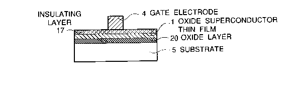
Then, as shown in ~igure 2D, an insulating layer 17 of SrTiO3
having a tllich~ess of 10 to- 20 nanometers is ~ormed on the c-axis oriented
YIBa2Cu3O7 ~ oxide superconduetor thin film 1 by a sputtering A
2 5 polycrystalline silicon layer 14 having a thickness of 200 nanometers is
~med on ~e insulating layer 17 by (:YD, as shown in Figure 2E.
- 13- ~15
.,9
Thereafter, the polycrystalline silicon layer l4 i8 etched by ~
reactive ion etching so as to fo~n a gate elec~rode 4, as shown in
Figure 2F. Then, the surfaces of the gate electrode 4 i~ oxidized so ax to
form a SiO2 layer havhlg a thickness of 50 to lOO nanometers, as showr
5 in Figure 2~}.
Therea~ter, as shown in Figure 2H, the hlsulating layer 17 of
SrTiO3 is etched so as to fo~m a gate insulating layer 7 by us~ng a mixture
of HF and NH40H. The mixture of HF ~nd NH40H selectively etched the
insulating layer 17 of Srl'iO3 and does not affeet the YlBa2Cu307 ~ ~xide
lO superconductor thin film l. The~efore, the characte~istics of the
YIBa2Cu307.~-oxide superconductor thin film 1 ;s maintained. A portion
of ~e YlBa2Cu307.g oxide superconductor thin film 1 under the gate
insulating layer 7 becomes a superconducting channel.
Thereafter, ~e substrate S is hea~ed ~o a temperature of 350 to 400
15 ~C under a pressure lower than 1 x 10⁻⁹ Torr so flS to clean ~e exposed
surface of ~e Yl}3a2Cu3C)7 ~ oxide supercollductor ~in film 1. 'rhis heat
~reatment is not necessary, if the exposed surface of ~e ~ axis oriented
Y~Ba2Cu307 ~ oxide superconductor thin film 1 is clean enough. Then, a
a-axis oriented Y1Ba~Cu307 ~ oxide superconductor thin ~llrn 11 having a
20 thic~ess of 500 nanometers is deposi~ed on t~ YlBa2Cu3Q7 ~ oxide
s~erconducto~ dlin film 1 by an off-axis sputtering so as to encapsu1a~e
~e gate electrode 4, as shown in Figure 2I. A condition of forming the
YlBa2Cu307 ~ sxide superconductor thin filrn 11 by an off-axis sputte
is as follows:
2 ~ Tempera~ure of ~e substrate 640 C
Sputten~g ~3a~ Ar: 90%
2: 10%
- 14 - 1~15g
2g'~ 9
Pressure 10 Pa
While the YlBa2Cu307.~ oxide superconductor thin film 11 is
deposited, silicon diffuses from the gate elec~rode 4 so as to fo~m a
insulating region 50 around the gate electrode 4. The insulating region 50
S is folmed of a YIBa2Cu307.~ oxide superconductor which does not show
superconductivity by ~e diffused silicon.
Finally, m o~de~ to planarize an upper surface of ~e YIBa2Cu307.~
oxide superconductor thin film 11, a photoresist layer (not shown) is
coated on ~e YIBa2Cu307 ~ oxide superconductor thin film 11 in such a
10 manner ~at the deposited photoresist layer has a flat upper swrface~ and
ihen, the coated photoresist layer and the Yl B a2Cu 30 7~ oxide
superconductor thin film 11 are etched back, until d~e upper surface of
the YlBa2Cu307~ oxide superconduc~or ~in film 11 is planar~zed and the
gate electrode 4 is exposed at the planarized upper surface of ~he
1 5 YlBa2Cu30~ ~ oxide supercondu~tor thin film 1 llas shown in Figure 2J.
Portions of ~e YIBa2Cu30? ~ oxide superconductor ghin ~llm 11 a~ the
bo~ sides of ~e gate ~lectrode 4 become a superconducting source region
2 and a superconducting drain region 3.
Metal electrodes may be fo~ned on the superconducting source
2 0 region 2 and the superconducting drain region 3, if necessary. With this,
~he super-FET in acco~dance wi~ the present inventioll is completed. .
The superconducting channel of ~e above mentioned super-FET
manufactured in accordance with the embodiment of the method of the
presel~t invention is formed on an oxide layer which has similar
2 ~ crystalline structure to that ~ the oxide superconductor. There~ore~ the
bot~om portion of the superconducting charmel is not degraded so that dle
- 15- ~5t59
~2~ g
substantial cross-sectional area of the superconducting charmel ~f the
super-FET is l~rger ~an that of a conventional ~uper-F~T.
Additionally, since supercondu~ting current flows ~long the
insulating region wbiGh is ~ormed by dif~used silicon next to the
S superconducting souree region and the superconducting drain region, the
superconducting current efficiently flows into and flows ~rom ~he
superconducting channel. By all of ~ese, the current capability of ~he
super-FET can be improved.
Furthe~nore, according to the present invention, the oxide layer,
l O the superconducting channe~, the gate insulating layer and the gate
electrode are self-aligned. The insulating region 50 which isolates the
gate electrode from the superconduc~ing source region and the
superconducting drain region is also automatically positioned. Therefo~,
~e limitation ~n the fine processing technique required for manufacturing
15 ~e supe~-~T is rela~ed.
Additionally, according to the present invention, ~he gate insulating
layer is ~ormed by an etching process using a mixtalr~ of HP and NH40H.
I'he mixture of HP and NH40H selec~ively etched ~e insulating layer of
SrTiO3 on the oxide superconductor thin film which will constitutes the
2 0 superconducting channel and does not affect the oxide superconductor thin
fi~m. ThereIore, the superconducting charac~eristics of the oxide
superc~nductor ~in fi}m is main~ined.
In ~e above mentioned embodiment, ~he oxide supercondlletor ~in
film can be formed of not only the Y-Ba-Cu-O compound oxide
2s supe~conductor material, ~ut also a high-TC (high critical temperalture3
o~ide superconductor material~ particularly a h;gh-TC copper-oxide ~ype
compound oxide superconductor material, for example a Bi-Sr-Ca~Cu-O
- 16 - t315~
:
2r'~ 9
compound oxide superconductor material, and a Tl-Ba-Ca-Cu-O
compound ~xide superconductor materi~l.
The invention has lhus been shown and described wi~ re~rence ~o
the specific embodiments. However, it should be noted ~hat ~e present
S invention is in no way limited to the details of the illustrated strucgures
bu~ converts aIId modi~lcations may be made wi~hin the scope of the
appended claims.
- 17- ~5