Note: Descriptions are shown in the official language in which they were submitted.
ZQ~3
TITLE OF THE INVENTION
Optical Disc and Method for Manufacturing the same
BACKGROUND OF THE INVENTION
1. Field of the Invention
The present invention relates to an optical memory
element for recording, reproducing, erasing information
using a laser beam and its manufacturing method, and more
particularly, to an optical disc having antistatic
properties and its manufacturing method.
2. Description of the Related Art
Recently, there are many researches and developments
for an optical memory element of a high recording density
and a large capacity. A glass and transparent resins are
suitable for substrates of the optical memory element and
especially polycarbonate is preferably suitable among the
resins, because it has a good productivity and moisture
resistance.
However, the polycarbonate substrate is easily attached
dust on its surface because it is easily electrically
charged owing to its high surface resistance of 1016 Q/~.
In an optical disc memory, a beam is focused on a recording
film in the order of ~m through the transparent substrate of
Z~?8~8~
approximately 1.2mm thickness made of glass or transparent
resins. Therefore, it is generally thought that the focused
beam is not affected by the dust on the transparent sub-
strate. But in actual case, the dust acts a lot on record-
ing and erasing of a magneto-optical disc, though it does a
little on playback of a Compact Disc as mentioned above. It
is because a lot of energy is consumed in recording and
erasing as compared with playback, and the dust causes to
scatter the beam on the substrate surface and make a record-
ing or/and erasing error as a result of energy power short-
age.
In order to prevent the beam from scattering as shown
Fig. 6, an optical disc is proposed to be covered with an
anti-static layer 42 where a metal oxide is dispersed as
electro-conductive filler in acrylic resin layer (Japan
Unexamined Patent No. 158643/1989) In addition, a recording
layer 44 is formed on a back surface of the polycarbonate
substrate 41.
But Fig. 6 is a schematic view showing the optical
disc. In actual case, both surfaces of the polycarbonate
substrate 41 are not even as shown in Fig. 7. More specifi-
cally, annular ridge 48 and groove 46 are formed at an inner
circumference on the front and back surfaces of the polycar-
bonate substrate 41, respectively corresponding to a gap or
a swelling in a joint between parts of a mold for injection
Z~3~8~
machine. In addition, a height of the ridge 48 and a depth
of the groove 46 are not uniform in the circumferential
direction. A centering part 45 called a center hub is
bonded on an inner hole 43 of the optical disc. The ridge
48 and the groove 46 are formed in the vicinity of outer
circumference of the centering part 45.
An antistatic layer is spin-coated on the surface of
the polycarbonate substrate 41. A density of the antistatic
layer changes in the circumferential direction corresponding
to a distribution of ridge height 48 or the groove depth 46.
As a result, antistatic layer changes in its thickness in
the circumferential direction, causing to shift the focused
optical beam offset, disturb a servo signal of recording,
reproducing and erasing, and decrease the power of the
optical beam.
When an antistatic layer 49 is formed outside the ridge
48 as shown in Fig. 7 in order to prevent wide distribution
of the film thickness of the antistatic layer, dust is
gathered at an exposed portion 47 where the antistatic layer
49 does not exist. Although the exposed portion 47 serves
to provide a reference surface when the optical disc is
mounted on a drive apparatus, the reference surface cannot
be provided or the polycarbonate substrate 41 is damaged if
the dust exists on the exposed portion 47.
In addition, the centering part 45 and the
2 0 8 5 3 8 3
polycarbonate substrate 41 are formed of the same material
so that their adhesive state may not be suffered from a
different expansion nor shrinkage by heat. More
specifically, the centering part 45 is also formed of
polycarbonate. Since an antistatic means is not taken in
the prior art, the dust is also attached to the centering
part 45. As a result, the dust is piled together on the
surface of the optical disc owing to peeling from centering
part 45 by a vibration of the disc or the like and causes to
disturb the servo signal and decrease the power of the
optical beam.
SUMMARY OF THE INVENTION
The present invention provides an optical disc
comprising a magneto-optical recording film and a protective
film formed in this order on one surface of a disc-shaped
plastics substrate of light transmission properties and an
antistatic film formed on the other surface to which an
optical beam is applied, and its manufacturing method.
Thus anaspect of the present invention provides an
optical disc comprising a recording film formed on a first
surface of a disc-shaped plastic substrate having light
transmission properties, and a coating formed on a second
surface of said substrate to which an optical beam is
applied, in which the substrate is made by injection molding
and includes a circular groove or ridge formed on the second
surface and substantially concentrically with the substrate,
a radius of the circular groove or ridge corresponding to a
radial distance between a center of an injection mold used
to form the substrate and a circular joint of the injection
3~
2~5~3
mold, the coating covering substantially the entire second
surface of the substrate, including the circular groove or
ridge.
A further aspect of the present invention provides
a method for manufacturing an optical disc in which a
recording film is formed on a first surface of a disc-shaped
plastic substrate of light transmission properties, and a
coating film is formed and coated by a liquid synthetic
resin having an electro-conductive filler on a second
surface of the substrate to which an optical beam is
~ applied, comprising the steps of: forming the substrate by
injection molding; forming a circular groove on the second
surface and substantially concentrically with the substrate,
the groove having a U-shaped cross-section and a radius
which corresponds to a radial distance between a center and
a joint of an injection mold used to form the substrate; and
coating the liquid synthetic resin to the portion of the
second surface laying outside of the groove, by rotation of
the plastic substrate at a first rotational speed, and then
coating the liquid synthetic resin to the portion of the
second surface laying inside of the groove by further
rotation of the substrate at a second rotational speed, in
which the second rotational speed is lower than the first
rotational speed.
The plastics substrate is formed by injection
molding and a groove or ridge is formed on the whole
circumference a radius of which is a distance between the
center and a joint position of an injection mold.
It is preferable that the antistatic film is formed
; ' ~'Z~
2~53~3
of a synthetic resin to which tin oxide doped with
phosphorous is added as an electro-conductive filler.
In addition, according to a manufacturing method
for an optical disc having the U-shaped groove, a liquid
synthetic resin is coated to an outer circumference of the
groove on the substrate surface by rotation and then it is
also coated to an inner circumference of the groove by also
further rotation, in which rotational speed during the
coating onto the outer circumference is higher than that
during the coating onto the inner circumference.
BRIEF DESCRIPTION OF THE DRAWINGS
Fig. 1 is a vertical sectional view showing a main
portion of an optical disc according to the present
invention;
Fig. 2 is an expanded vertical sectional view
showing a part of the optical disc shown in Fig. 1;
Fig. 3 is a vertical sectional view showing a main
portion of another optical disc according to the present
invention;
Fig. 4 is a vertical sectional view showing a main
portion of a another optical disc according to the present
invention;
Fig. 5 is a vertical sectional view showing a main
portion of still another optical disc according to the
present invention;
Fig. 6 is a schematic vertical sectional view
showing a conventional optical disc; and
~P
z~
Fig. 7 is a vertical sectional view showing a main
portion of the conventional optical disc.
DETAILED DESCRIPTION OF THE INVENTION
The optical disc according to the present invention may
be any one of a magneto-optical disc, a compact disc, a
write once type disc and a photochromic type disc which are
all well known.
The recording film, the protective film, the moisture
resistance film for protecting moisture transmission, and
the antistatic film formed on the optical disc will be
described hereinafter.
The plastics substrate having light transmission
properties according to the present invention is formed by
normal injection molding. A material of the substrate may
be plastics which has light transmission properties and is
not likely to be distorted. Typically, polycarbonate is
suitable. Another material such as acrylic resin or epoxy
resin may be also suitable for the substrate. A thickness
of the substrate is normally 1.15 to 1.25mm.
Since the plastics substrate is formed by the injection
molding, a joint between parts of a mold is generated.
Although a position of the joint varies with a design of the
mold, normally it is between 1/10 and 4/5 of the radius of
the substrate. A U-shaped groove or ridge is formed in
whole circumference corresponding to the position of the
2~
joint. The groo~e or the ridge may be formed by using the
mold which previously installs it on a predetermined posi-
tion, or may be shaped on the joint position of the plastics
substrate after the injection. In a case of the groove, the
joint is positioned in the middle the groove. A dimension
of the groove in cross section is preferably as follows.
That is, a width of an opening is approximately 1.5 to
2.5mm, a width of bottom is approximately 0.7 to 1.3mm and a
depth is approximately 0.1 to 0.2mm. Meanwhile, a dimension
of the ridge in cross section is preferably as follows.
That is, a width of bottom is approximately 1.5 to 2.Omm, a
width of top is approximately 0.7 to 1.3mm, and a height is
approximately 0.3 to 0.7mm.
The recording film is formed on one surface of the
plastics substrate by spin coating, roll coating,
sputtering, or other coating methods. The structure of the
recording film is well-known in the prior art. Typically,
there are a four-layer structure such as AlN/GdTbFe/AlN/Al
or AlN/DyFeCo/AlN/Al or a three-layer structure such as
SiN/TbFeCo/SiN or SiAlON/TbFeCo/SiAlON. The film thickness
thereof is normally 150 to 300nm. Although the recording
film is formed on the whole surface of the plastics
substrate, it may be formed partially thereon.
In addition, the recording film serves as not only the
magneto-optical medium but also a medium of read only, write
once, phase transition or photochromic.
The protective film is formed on the recording film by
spin coating, roll coating, or other coating methods. The
protective film mainly protects the recording film, which
may be formed of acrylic urethane UV curing resin,
polyvinylidene chloride resin, poly-trifluoride ethylene
chloride resin or the like. The film is formed by coating
those. Its film thickness is normally 2 to 20~m.
In addition, the moisture resistance film is optional-
ly formed on the other surface of the plastics substrate to
which the optical beam is applied by spin coating, roll
coating, vapor deposition, sputtering or the like. The
moisture resistance film may be formed of an inorganic
material such as AlN, SiN, ZnS, Al203, SiO2, SiAlON or an
organic material such as polyvinylidene chloride resin or
poly-trifluoride ethylene chloride resin. Among them, AlN
is especially preferable. A thickness of that film varies
with the material. Generally, the thickness of the film
formed of the inorganic material ranges from 1 to 300nm,
preferably 1 to 200nm. Alternatively, the thickness of the
film formed of the organic material ranges from 2 to 20~m,
preferably 2 to 15~m. For example, in a case of AlN, it
preferably ranges from 1 to 20nm. Within the above range of
the film thickness, transient warp on change in humidity can
be prevented and also an interference band of the optical
2Q~
disc can be prevented.
In addition, the antistatic resin film mixed with an
electro-conductive filler is formed on the other surface of
the substrate or on the moisture resistance film optionally
formed on the other surface to which the optional beam is
applied. The antistatic resin film mixed with the electro-
conductive filler can be formed by mixing a synthetic resin
or its raw material with the transparent electro-conductive
filler in a predetermined ratio and, if necessary, adding an
inorganic filler a little to improve the hardness, and
coating them onto the substrate. As the synthetic resin,
for example, acrylic urethane W curing resin, acrylic W
curing resin or the like is suitable.
The film is formed by coating onto the substrate by,
for example spin coating, curing by means such as W ray
irradiation, heating and cooling. The method of forming
film may be varied according to the synthetic resin
employed. In a case where the U-shaped groove is provided
in the substrate, a liquid synthetic resin is coated to the
outer circumference of the groove on the substrate surface
by rotation, then coated to the inner circumference of the
groove on the substrate surface by further rotation, and
finally the groove is filled up to be nearly even. It is
preferable that the rotational speed while the liquid syn-
thetic resin is coated to the outer circumference is approx-
2~
imately 2,000 to 4,000rpm, the rotational speed while it iscoated to the inner circumference is approximately 300 to
800rpm and the rotational speed while the groove is filled
up is approximately 20 to 80rpm. At this time, the rota-
tional speed during the coating onto the inner circumference
has to be lower than that during the coating onto the outer
circumference. If the rotational speed during the coating
onto the inner circumference is higher than that during the
coating onto the outer circumference, the liquid synthetic
resin for the inner circumference overflows to the outer
circumference beyond the groove, which causes to take place
a bad influence on uniformity of the antistatic film thick-
ness.
The film thickness is preferably 1 to 20~m. The
antistatic resin film contains a transparent electro-conduc-
tive filler and prevents the dust from being attached onto
the surface of the optical disc and also prevents a damage
from being generated, and it is preferable that its film
surface has high hardness and relatively low surface resist-
ance. The hardness is preferably HB or more in pencil
hardness. In addition, the surface resistance is preferably
approximately 1013Q/o or less.
The transparent electro-conductive filler preferably
comprises tin oxide doped with phosphorus because light
transmission properties and stability can be provided at the
2~5~83
same time. In addition, doping of phosphorous, such as
phosphoric acid or sodium phosphate, to the tin oxide is
performed by corecipitation and sintering from a liquid
phase. A doping amount into the tin oxide is preferably 3
to 7wt% of the whole amount of the electro-conductive
filler. If the doping amount is less than 3wt~, the
electro-conductivity becomes poor and its stability becomes
also poor. It is preferable that the content of the
electro-conductive filler in the antistatic film is about 25
to 45wt% and the average particle diameter of the filler is
0.15~m or less. If the content of the filler is less than
25wt%, the surface resistance exceeds 1013Q/o, so that
enough antistatic performance can not be obtained. If the
content of the filler exceeds 45wt% or the average particle
diameter is larger than 0.15~m, surface roughness of the
film is increased and then the light transmission properties
become poor.
Although the optical disc according to the present
invention is t~pically a magneto-optical disc, it may be a
compact disc, a write once type disc and a photochromic type
disc using a photochromic material as the recording film.
EXAMPLE
Example 1
An embodiment of the present invention will be
described in reference to Figs. 1 and 2.
, ~
~ .~
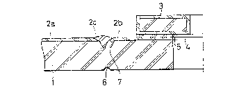
Reference numeral 1 designates a substrate formed of
polycarbonate, reference numeral 2a designates an outer
circumferential portion of an antistatic film, reference
numeral 2b designates an inner circumferential portion of
the antistatic film, reference numeral 2c designates the
antistatic film formed on the groove, reference numeral 3
designates a positioning part, reference numeral 4 desig-
nates another antistatic film, reference numeral 5 desig-
nates an adhesion layer, reference numeral 6 designates a
small groove generated by a joint on the other surface of
the polycarbonate substrate, reference numeral 7 designates
a U-shaped groove on one surface of the polycarbonate sub-
strate according to the present invention, and reference
numeral 8 designates a ridge generated by the joint on one
surface of the polycarbonate substrate.
As shown in Fig. 1, the antistatic layers 2a to 2c are
formed on one surface of the polycarbonate substrate 1 onto
which a laser beam used for recording, reproducing and
erasing is applied, and a recording layer (not shown) is
formed on the other side of the substrate. The small groove
6 and the U-shaped groove 7 are formed on the back surface
and on the front surface of the polycarbonate substrate 1,
respectively at a position corresponding to the joint
between parts of the mold used for injection of the
polycarbonate substrate 1. A width of an opening of the
2~
groove 7 is approximately 2 mm, a width of a bottom thereof
is approximately lmm, and a depth thereof is approximately
O.l to 0.2 mm. In addition, the small ridge 8 is formed by
the joint in the bottom thereof as shown in Fig. 2.
Steps of forming the antistatic layers 2a to 2c will be
described hereinafter. First, an antistatic agent is
applied outside the groove 7 by spinning to form the
antistatic layer 2a. The rotational speed may be set high,
for example 300Orpm in order to form the thin and uniform
antistatic layer 2a. In addition, a mixture of the W
curing resin and a filler of tin oxide doped with phosphorus
is used as the antistatic agent.
Then, the antistatic agent is coated inside the groove
7 by spinning to form the antistatic layer 2b. Since it is
important that the antistatic layer 2b does not overflow
beyond the large groove 7 rather than it is uniformly
formed, the rotational speed at that time is set low, for
example 500rpm.
Finally, the antistatic agent is coated in the groove 7
at considerably low speed, that is, several tens rpm to form
the antistatic layer 2c, whereby the antistatic layer 2a and
the antistatic layer 2b are made even by coating the anti-
static layer 2c on the groove 7 and then they are electri-
cally conductive. Thus, the groove 7 takes an active part
as a barrier of the antistatic agent fluid.
In the above embodiment of the present inven~ on, the
antistatic layer 2a has to be coated before the antistatic
layer 2b is coated. That is, when the antistatic layer 2b
is coated, the antistatic agent sometimes partially
overflows beyond the large groove 7. If the antistatic
layer 2a is coated onto the overflowed layer, the film
thickness of the antistatic layer 2a is not even, which
causes a servo-mechanism disturbed.
Then, the center hub 3 of polycarbonate is covered with
the antistatic layer 4 as same material as the antistatic
layers 2a to 2c and bonded to the antistatic layer 2b
through the electro-conductive adhesion layer 5. As the
electro-conductive adhesion layer 5, an electro-conductive
adhesive in which tin oxide is mixed in the W curing resin
(ELCOM p3555 made by CATALYSTS & CHEMICALS INDUSTRIES CO.,
LTD.) is employed.
As described above, since the small ridge 8 is formed
in the groove 7 as the result of the joint and the anti-
static layers 2a, 2b and 2c are formed in this order, the
antistatic layer 2a to which the optical beam for recording,
reproducing and erasing is applied can be uniformly formed.
Furthermore, since the antistatic layer 2b is formed on a
reference surface when the optical disc is attached onto a
drive apparatus, the dust is not attached onto the reference
surface.
14
2 ~ ~3~
If the antistatic agent is doped with phosphorus,
transparency of the antistatic layers is improved and the
surface resistance of the antistatic layer becomes small
(approximately 101~Q/c). Especially, when the W curing
resin is used as the antistatic agent, its transparency is
important and doping of phosphorus is effective.
Example 2
Another embodiment of the present invention will be
described hereinafter in reference to Fig. 3. Parts having
the same functions as in the above embodiment are denoted
the same reference numeral as above and its description will
be omitted. Reference numeral 9 designates a ridge.
The U-shaped ridge 9 is formed on the surface of the
polycarbonate substrate 1 at a part corresponding to the
joint of the mold as shown in Fig. 3. A width of the ridge
is approximately lmm, a height thereof is approximately
0.5mm. The antistatic layers 2a, 2b and 2c are coated to
the outer and the inner circumference and on the ridge 9,
respectively by spinning. Conditions of the above coating
is the same as described in the above embodiment 1.
As described above, the ridge 9 serves as a barrier for
preventing fluid of the antistatic layer 2b from overflowing
toward the antistatic layer 2a when the antistatic layer 2b
is coated. Similar to the embodiment 1, the antistatic
layers 2a and 2b are electrically conductive through the
2~5383
antistatic layer 2c.
When the surface resistance of the antistatic layers 2a
to 2c according to the present invention is approximately
1013Q/~, even if the antistatic layer 2c is not provided,
which does not affect on their antistatic faculty. However,
when the surface resistance is in the order of lO10Q/G, if
there is not provided the antistatic layer 2c to make elec-
trically conductive passage to the outside through the
center hub 3, their antistatic faculty becomes poor.
In order to make electrically conductive passage to the
outside, a cartridge for housing the optical disc is formed
of the electro-conductive polycarbonate and the antistatic
layers 2a to 2c are provided on the optical disc, whereby
the whole surface is electro-conductive. Thus, there is no
potential difference between the optical disc and the
outside when the cartridge is carried.
Although the optical disc normally floats during
rotation by the drive unit, the potential difference between
the optical disc and the outside is reconciled through the
center hub 3.
Furthermore, if an electro-conductive brush is provided
within the cartridge in contact with the surface of the
optical disc during rotation, the antistatic effect becomes
more conspicuous.
In addition, when the antistatic layer 2b is coated by
~'
the brush or formed by screen printing process on the inner
circumference after the antistatic layer 2a is coated by
spinning according to the embodiments 1 and 2, although
uniformity of the antistatic iayer 2b is not obtained,
sufficient characteristics as the antistatic layer according
to the present invention can be obtained.
Example 3
According to this embodiment of the present invention,
an electro-conductive film is employed in stead of the
antistatic layer used in the above embodiments 1 and 2.
Figs. 4 and 5 show an example. The same reference numeral
as the above is not described here. Reference numeral 10
designates an electro-conductive film, reference numeral 11
designates an electro-conductive adhesion layer, and
reference numeral 15 designates a part corresponding to the
joint between parts of the mold. As shown in Fig. 4, in
stead of the antistatic layer 2b, the electro-conductive
film 10 may be adhered to a region inside the small ridge 8
through the electro-conductive adhesion layer 11. The
electro-conductive film 10 is formed of an ITO (oxide of
indium and tin whose thickness is approximately 0.07~m) on a
polyester film (whose thickness is approximately 50~m). As
the electro-conductive adhesion layer 11, the electro-
conductive adhesive, which is the same as the electro-
conductive adhesive used in the embodiment 1, in which tin
oxide is mixed with the W curing resin ( ELCOM p3555 made by
CATALYSTS & CHEMICALS INDUSTRIES CO., LTD.) is used.
The center hub 3 at the inner circumference of the
optical disc according to the embodiments 1 to 3 may be
formed by injecting a resin in which a cationic antistatic
agent is mixed in polycarbonate. In this case, if the ridge
is provided on an adhesive surface of the center hub 3 and
the center hub 3 is welded to the optical disc by supersonic
wave, the electro-conductive adhesion layer 5 may be omit-
ted.
Since the small ridge 8 shown in Fig. 4 is so small,
the part 15 corresponding to the joint can be made almost
even by only rubbing it with alumina of 0.5~m several times
as shown in Fig. 5. Then, the antistatic agent is applied
from the inner circumference by spinning. Thus, the uniform
antistatic layer is formed.
As described above, according to the optical disc, an
groove is formed at a position on a pl stics substrate
corresponding to the joint so as to take an active part as a
barrier of a liquid material fluid coated to the plastics
substrate.
Therefore, since the surface of the plastics substrate
is separated to an outer and an inner circumferential region
by the groove or ridge, the liquid material can be coated to
18
2~
each region without affected by the joint between parts of
the mold for injection. In addition, since the groove takes
an active part as a barrier of the liquid material fluid
when the liquid material is coated to the inner circumferen-
tial region by, for example spin coating, the liquid materi-
al coated to the inner circumferential region is prevented
from overflowing to the outer circumferential region.
Furthermore, dust is prevented from being attached onto
the surface of the positioning part, whereby recording and
reproducing reliability of the optical disc can be improved.
Still further, transparency of the antistatic layer can be
improved by doping the tin oxide filler with phosphorus.
While only certain presently preferred embodiments have
been described in detail, as will be apparent with those
skilled in the art, certain changes and modifications can be
made without departing from the scope of the invention as
defined by the following claims.