Note: Descriptions are shown in the official language in which they were submitted.
208423
PHN 13926 1 21.04.1992
Solid state imaging device and camera provided with such an imaging device.
The invention relates to a solid state imaging device comprising a system
of sensor elements arranged in rows and columns for converting radiation into
electric
charges which can be transported parallel to the column direction by vertical
transport
means to a horizontal readout register in the form of a charge-coupled device
into which
the charges are entered row by row and subsequently read out at an output of
the
horizontal register during a certain time interval, called active line time
hereinafter,
means being present by which the device can be set in either of two states,
whereby in a
first state the signals from all columns of the system are used and in the
second state the
signals from a number of columns are not used. The invention also relates to a
camera
provided with such an imaging device.
The device may in this cave be formed by a monolithically integrated
circuit in which the sensor elements in the form of photodiodes or MOS diodes
are
accommodated together with the vertical transport means and the horizontal
readout
register in a common semiconductor body made of, for example, silicon. The
vertical
transport means are usually formed by charge-coupled devices which either
coincide
with the photosensitive elements, such as, for example, in the case of frame
transfer
sensors (F"T sensors), or are provided interposed between columns of separate
photosensitive elements (interline sensors). In alternative embodiments, the
photosensitive elements and the horizontal register may be manufactured in
different
semiconductor bodies, for example, when requirements are set for the
photosensitivity
which are not compatible with the requirements set for the readout register.
It is noted
here that the terms "horizontal" and "vertical" are to be understood in a
relative sense
only, not in an absolute sense, merely indicating that the transport in the
readout
register is transverse to the transport by the said transport means.
The possibility of effectively switching off a number of columns renders
it possible to obtain an imaging device which satisfies the requirements of
different
standards, so that it is not necessary to design an adapted device and/or
camera
separately for each standard.
PHN 13926 2 2 O g ~ 4 2 3 21.04.1992
US Patent 4,426,664 discloses a charge-coupled imaging device of the
kind mentioned in the opening paragraph which can be used both in the NTSC
system
and in the PAL or SECAM system. The imaging device is for this purpose
provided
with as many rows and columns as are necessary for use in the PAL or SECAM
system. For use in the NTSC system, a number of lines as well as a number of
columns
are not used in that the electric charge generated in the relevant columns is
drained off
instead of being processed further as video information. For this purpose, the
readout
register is coupled at one end, i. e. the left-hand end, to an output terminal
where the
video information can be derived, and at the opposite end, so the right-hand
end, to a
drain for draining off the information which is not used. This charge is
generated in a
strip of columns at the right-hand side of the imaging device. During
operation in the
NTSC setting, a full line including the unnecessary charge packages from the
strip of
columns mentioned above is transported into the readout register each time.
The active
video information is transport~l to the left during the active line time in
order to be
read out. Simultaneously, the transport d:~rection is reversed in the portion
of the
readout register in which the non-active information is stored, so that the
relevant
charge can be drained off at the right-hand end of the readout register.
One of the disadvantages of such a device is that the optical centre in at
least one of the two states does not coincide with the centre of the portion
of the
imaging device which is in use. The luminous intensity is generally Mghest in
the
optical centre in a system of lenses, such as in a camera, and decreases
towards the
edges to a value which is visibly lower at the edges. A similar profile is
often found in
the resolution of the optical system. This non-uniform intensity, possibly
coupled to a
decreasing resolution, is not unpleasantly noticeable during display as long
as the
intensity and the resolution are highest in the centre of the displayed
picture. If,
however, the centres do not coincide, as is the case in the imaging device
described
above, the intensity maximum, and possibly the resolution maximum, will not
lie in the
centre during picture display, which will in general be felt to be very
unsatisfactory.
Such problems may also occur in situations other than that described
above, when the information from a number of columns is not used. Thus it is
very
important for the optical centre of the lens to coincide always with the
centre of the
imaging device when a zoom lens is used.
~~3~~4~~
PHI~T 13926 3 21.04.1992
The invention has for its object inter alia to provide an imaging device of
the kind mentioned in the opening paragraph whose centre does not or at least
substantially not change its place when the number of columns used is changed.
According to the invention, an imaging device of the kind mentioned in
S the opening paragraph is characterized in that the columns not used in the
second state
of the device form two strips of columns on either side of the system, the
charges
derived from these columns being transferred to the horizontal readout
register
simultaneously with the charges from the columns which are used and being
drained
from the register in a time interval which lies between two consecutive active
line
times. Since the non-active information is not drained in the active line
time, it is
possible to define a strip of columns also at the side of the output amplifier
whose
charges or information/signal packages are not used. The charge packages from
these
columns are transported into the readout register simultaneously with the
active
information and drained off before the start of the active line time without
interfering
with the active information.
The charge packages coming from the strip of columns at the opposite
edge, so farthest removed from the output amplifier, can be drained off in the
manner
described above through a reversal of the transport direction. An alternative
embodiment, in which this reversal of the transport direction is not
necessary, is
characterized in that, in the said second state, the charges coming from the
unused
columns are transported into the horizontal register in the same direction as
the used
columns and are drained off partly before the active line time in which the
used charges
are read out and partly after this active line time. Preferably, these
packages are drained
off together with non-active information from the next row after the next row
of
information has been transported into the readout register. An embodiment
which has
the advantage that the number of transport steps is reduced in that charge
packages of
non-active information from two consecutive rows are partly joined together,
is
characterized in that the horizontal register is provided with charge storage
locations
having a charge storage capacity which is at least substantially double the
charge storage
capacity of the sensor elements. The charge storage capacity may be determined
in
various manners, for example, through the width of the gate electrodes and of
the
channel.
According to an important aspect of the invention, it is possible to adjust
CA 02085423 2001-03-05
20104-8761
4
the width/height ratio of a solid state imaging device. Usual
imaging devices have a width/height ratio of 4 to 3, analogous
to the ratio of a TV screen. In the near future there will
also be TV receivers on the market having a relatively greater
width, the said ratio becoming 16 to 9 then. The picture ratio
of the imaging device must be a corresponding one for such
systems. It would be expensive and complicated if TV studios
were to require two types of camera for these two types of
pictures. The application of the invention renders it possible
to design an imaging device with a 16 to 9 image ratio, having
a central portion having a 4 to 3 image ratio which has a
sufficient resolution for the present standard, for example,
750 pixels per line with two added portions of, for example,
125 pixels per line on the left and on the right. An important
embodiment of a solid state imaging device according to the
invention is characterized in that the system has a
width/height ratio of at least approximately 16 to 9 in the
first state and in that the width/height ratio of the system
minus the columns not used in the second state is at least
approximately 4 to 3.
The invention may be summarized as a charge-coupled
solid state imaging device comprising a system of sensor
elements arranged in rows and columns for converting photo-
radiation into electric charges which are transported parallel
to the column direction by vertical charge coupled transport
means screened against radiation and forming a memory for
storing charge packets generated in the sensor elements to a
single horizontal readout register comprising a charge-coupled
device into which the charges are entered row by row and
subsequently read out at an output of the single horizontal
CA 02085423 2001-03-05
20104-8761
4a
register during an active line time interval, means for setting
the device in a selected one of two states to obtain a desired
image aspect ratio, a first state for obtaining a first image
aspect ratio of at least about 16 to 9 in which the signals
from all columns of the system are used and a second state for
obtaining a second image aspect ratio of at least about 4 to 3
in which the signals from a number of columns are not used,
wherein the columns not used in the second state of the device
form two strips of columns on two opposite ends of the system,
the charges derived from these columns being transferred to the
single horizontal readout register simultaneously with the
charges from the columns which are used and subsequently being
drained from the register in a horizontal blanking interval
which lies between two consecutive active line time intervals
to increase a frame rate of the imaging device, and wherein in
said second state, the charges coming from the unused columns
are transported into the horizontal register in the same
direction as the used columns and are drained off partly before
the active line time interval in which the used charges are
read out and partly after this active line time interval.
The invention will be explained in more detail with
reference to a few examples and the accompanying diagrammatic
drawing in which:
Fig. 1 is a diagram of a solid state imaging device
according to the invention;
Fig. 2 is a time diagram of the device of Fig. 1
during operation; and
Fig. 3 is a diagram of a second embodiment of an
imaging device according to the invention.
CA 02085423 2001-03-05
20104-8761
4b
The invention will be described with reference to a
charge-coupled imaging device of the frame transfer (FT) type,
although the imaging device may equally well be of another type
which is know per se, as will be apparent from the following
description, such as the IL type (inter line) or of the IL type
with frame transfer. In this last type, an additional memory
of the size of one raster is provided between the sensor
section (rows and columns of photodiodes with interposed
vertical transport channels) and the horizontal output
register, into which extra memory the entire raster is written
after integration in a time which is small compared with the
integration time.
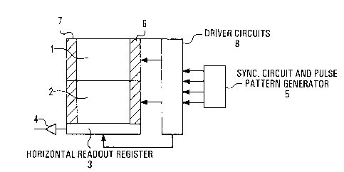
The image sensor is of a construction which is known
per se, comprising
~0~~42~
PHN 13926 5 21.04.1992
a photosensitive integration section 1, a memory section 2 screened against
radiation,
and a horizontal output register 3. The charge packages are transported row by
row
from the memory section 2 into the output register 3 and are subsequently
transported to
the left in the register 3 and read out through the output amplifier 4 in a
time interval
which will be called active line time hereinafter.
For operating the device, means 5 are provided by which the imaging
device can be set for one of at least two states. In the first state, the
signals from the
entire matrix of the imaging section 1 are used as active video information;
in the other
state, the information generated in a number of columns is not used as active
video
information and should accordingly be drained off in some way. According to
the
invention, the columns whose information is not used in the second state are
arranged in
two strips 6 and 7 situated on either side of the matrix formed by the imaging
section
and the memory section. These strips have been hatched in Fig. 1 for greater
clarity.
The centre of the portion of the imaging section which is used does not change
its place
when the system is switched from the one state into the other state, and can
accordingly
coincide with the optical centre of the optical system (not shown in the
drawing) in
either state. This configuration is possible because the charge packages in
the columns
7, which are placed in the horizontal register 3 simultaneously with the
active
information, are drained off through the output of this register in a time
interval which
lies before the active line time belonging to this line and after the active
line time of the
preceding line. This time interval will be referred to as horizontal flyback
time
hereinafter on the analogy of the terminology in picture display systems.
The invention may be used in various situations in which the dimensions
and/or the relative dimensions of the image are to be changed. In the present
embodiment, the aspect ratio may be set as desired by means of the invention.
The
width/height ratio of the non-hatched portion of the imaging section 1 is at
least
substantially 3 to 4, the number of columns of this section being, for
example, 720. The
width of the strips 6 and 7 is so chosen, for example 130 columns, that the
width/height
ratio of the imaging section 1 including the strips 6 and 7 changes into 16 to
9.
The signals which determine whether the device is operated in the one or
in the other state are generated by the block 5 which may comprise inter alia
a
synchronization circuit (sync. pulse i.c.) and a pulse pattern generator (ppg
i.c.). The
block 5 controls the block 8 which comprises a number of driver circuits which
supply
PHN 13926 6 21.04.1992
the required clock voltages for the imaging section 1, the memory section 2,
and the
readout register 3.
In the diagram of Fig. 2a, T, indicates the active line time and Tb the
flyback time. The active line time T, is, for example, 52 .sec, the flyback
time Tb is,
for example, 12 sec. If the imaging device is operated for the 16 to 9 ratio,
so that the
information of all 980 columns is used as active video information, a line
from the
memory 2 is put in the readout register 3 during the flyback time Tb each
time. The
charge packages of this line are subsequently re<~d out in usual manner in the
active line
time T, with a frequency of, for example, 19 MHz. When the imaging device is
operated in the 3 to 4 state, so that the 260 columns in the strips 6 and 7
are not used,
the clock frequency of the readout register 3 is reduced to, for example, 14
MHz.
During the time T~ (Fig. 2b), which is, for example 2.5 ~csec, an entire line
including
charge from the columns 6 and 7 is put in the readout register 3. In the
remaining 9.5
~csec of the flyback time Tb, indicated with Td in Fig. 2c, the 130 charge
packages
coming from the strip 7 are drained off by means of the usual charge transport
in CCDs
at a frequency of 14 MHz. Then the 720 charge packages from the central
portion of
the device are read out during the active line time T, (see Fig. 2c) and used
as active
video information. After the active line ti me T" when the said 720 signals
have been
read through the amplifier 4, charge transport is stopped. The last 130 charge
packages
coming from the strip 6 are still in the readout register 3 at the level of
the strip 7. In
the ensuing period T~, which forms part of the next flyback time, the next
line of video
information is moved from the memory 2 into the output register 3. The charge
packages from strip 7 are added to the charge packages from strip 6 still
present from
the preceding line in the output register 3. During the remainder Td of the
flyback time,
the 130 charge packages just joined together are drained off, after which the
720 signals
from the central portion of the imaging section are read out in the active
line time. In
this manner, the entire 4 to 3 matrix can be read out, while the non-active
information
from the strips 6 and 7 is entirely drained away during the flyback time.
It is noted that it is not necessary in principle to join together the charges
from the strips 6 and 7. Thus, for example, the output register 3 may be
extended at the
side facing the amplifier 4 by a number of extra storage locations in which
the charge
packages from the strip 6 are stored before a new line is transported into the
output
register, after which, in the flyback time, these charge packages are drained
off
PHN 13926 7 ~ ~ ~ ~ ~ ~ J 21.04.1992
followed by the charge packages from strip 7. In an alternative embodiment, an
output
register identical to that in Fig. 1 is used, and the charges coming from the
strip 6 are
drained off immediately after the active line time and before a new line is
placed in the
register 3. In both embodiments, however, draining of the excess charge
packages does
require extra transport steps and time. If the ch~~rge packages are added
together, as in
the embodiment described, draining takes only 130 instead of 260 transport
steps. The
storage capacity in at least the 130 storage locations situated in from of the
output of
register 3 must be sufficiently large for accommodating double the charge
packages of
maximum size in the imaging secdon/memory section. In the simplest embodiment,
this
is achieved by adaptation of the width of the register 3. Obviously,
alternative known
techniques, such as the choice of the dopant concentration and/or the value of
the
applied clock voltages, or combinations of various methods may be used.
In the embodiment described here, the removal of the excess charge
packages takes place with the same clock frequency as reading of the active
information. If this method takes compa~~atively too much time, for example,
in view of
the time required for transferring the ch~~rge from the memory section into
the register
3, a higher clock frequency may be used for the removal of the charge from the
strips 6
and 7 than for reading the active information. The said 19 MHz clock voltage
with
which the information is read out in the case in which the aspect ratio is
16/9 may
advantageously be used for draining off the excess charge. The time required
for
draining off 130 packages is then only approximately 6.8 sec, so that more
time is
available for the memory-output register transport.
Fig. 3 diagrammatically shows an embodiment of a solid state imaging
device according to the invention in which the excess charge packages from the
strip 6
(when the width/height ratio is 4/3) are not transported to the output
amplifier 4, but
are removed through an extra output 10 at the side remote from the amplifier
4. In this
arrangement, the clock voltages to the gates (not shown) in the portion 11 of
the
register 3 are applied in a different order compared with the clock voltages
at the gates
of the remaining portions 12-13 of the register 3, so that the charge
transport in the
portion 11, at least during the flyback time for draining off the excess
charge from strip
6, is to the right, while it is to the left in the portions 12 and 13. When
the portion 11
of the register 3 is empty, while at the same time the excess charge from
strip 7 was
drained off through the output at the left-hand side of the register, the
clock voltages in
20~~4~3
PHN 13926 8 21.04.1992
the portion 11 may or may not be stopped, while; the charge transport in the
portions 12
and 13 is continued in the active line time for reading out the active
information. When
the imaging device is operated in the width/height ratio 16/9 state, the
charge transport
direction in the portion 11 is reversed in that the portion 11 receives the
same clock
voltages as the portions 12 and 13, so that the entire line can be read out
through the
amplifier 4.
Since charge transport must be possible in two directions in the portion
11, an output register is preferably used without a built-in transport
direction, as is
often the case in 2-phase CCDs. A 3- or 4-phase CCD may accordingly be
advantageously used for the register 3.
It is noted that the matrix 14 is shown as being adjacent to the register 3
in Fig. 3 of the imaging device. The region 14 may correspond to the memory
section 2
of the preceding embodiment. In an alternative embodiment, in which a separate
memory section is not necessary, the region 14 may correspond to the imaging
section 1
in Fig. 1. In the case of an interline sens~;~r, the region 14 is formed by
columns of
photodiodes, interspaced by vertical transport lines coupled to the register
3.
It will be clear that the invention is not limited to the embodiments
described here, but that many more variations are possible to those skilled in
the art.
Thus the width/height ratio may vary in a different manner than the conversion
between
the 4/3 standard and the 16/9 standard described here. It is also possible to
combine a
reduction in the width of the picture as described above with a reduction in
its height.