Note: Descriptions are shown in the official language in which they were submitted.
wn~2/01948 ~ V PCT/US91/03216
TECHNIQU~ ~OR D~MODULATING AND D~CODING MLS DP5
TRANSMISSIONS USIR~ A DIGI$AL SIG~AL PROCESSOR
The U.S. Government has rights in this
invention pursuant to Air Force Contract No.
Fl9628-87-C-0l99
~c~orouC~ of the In~ention
Pield of the In~ention
The present invention relates to the
Microwave Landing System. More particularly the
present invention relates to detecting, demodulating
and decoding the Differential Phase Shift Keying
(DPSK) tr3nsmissions of function identification and
data transmissions associated with the international
. standard Microwave Landing System (MLS).
~ÇscriDtion of the Prio~-AL~
The Microwave Landing System (MLS) is an
internationally standardized means to provide
precision approach and landin~ guidance to properly
; 25 equipped user aircraft. The MLS signal format as
` illustrated in Fiqures l - 3 consists of a series o~
-~ guidance and data.functions transmitted in a
time-division-multiple~ (TDM) signal format on a
single one of 200 channels in the microwave C-band
(5030-5090 Mhz). The signal format is radiated by
ground stations located at the airport and received
by special equipment t~ithin the user aircraft.
......
WO92/~1948 PCT/U591/03216
-2~
Each MLS function slot is identified by a
unique digital code transmitted as part of the
~unction preamble using DPSK encoding Each digital
; bit is 64 usec wide, for an ef~ective digital data
rate of 15,625 bits~sec.
The function preamble for all MLS functions
is divided into at least three sections, as shown in
Figure 4. The first 13 bit period (832 usec)
consists of an unmodulated carrier which is
equivalent to a string of binary zeros encoded into
DPSK. This is followed by a five bit digital 3arker
Code (lllOl) for time synchronization. Finally, a
unique seven bit function identification code,
consisting of five data and two parity bits, is sent
to identify the ensuing MLS function.
Many classical tests on communications
theory such as Commsnic~ Svstems and Techni~ues,
by Schwartz, M., ~ennett, W.R., and Stein, S., McGraw
- Hill Book Co., New York, 1966, illustrate the
simple, straightforward means of DPSK decoding shown
in Figure 5. In this approach, a delayed version of
the received signal is used as the reference
oscillator in a coherent detector. The coherent
detector output is proportional to the phase
difference between this reference and the current
received signal, i.e., between the current and
previous DPS~ bits. The actual numerical output of
the coherent detector depends on the total electrical
phase of the intermediate frequency (IF) signal,
wifT, over the period, T, of a single DPSK bit, where
Wif is the angular frequency of the IF signal in
radians/sec and T is measured in seconds.
: .
,
. ~ .
.
W~92/01948 PCT/U591/03216
-- 20~50
As noted in ~mmgmsation SYstems and
Technigues (cited above~ and elsewhere, this
technique is applicable only in cases where the
frequency error in Wif is small. If the frequency
error, Eif is not small, the total phase (wi~+ Eif)T
can vary significantly from the e~pected result. In
the e~tremes, the output of the coherent detector in
Figure 5 could be zero (when (wif~if)T ~ ~/2) or the
state o the information bits could be reversed (when
(Wif+~if )T.Jt) .
In the MLS application, even a perfect
receiver could e~perience frequency errors which
e~ceed these limits, due to ground station frequency
stability and aircraft motion doppler. This is
discussed in Anne~ 10 to the Convention on
International Civil Aviation, Volume 1, Chapter 3.11,
ICAO, Montreal, Oct. 1987, as well as ~inimYm
O~erational Performance Standards for Microwave
Landina Svstem Airborne Receivina EouiDmen~, DO-177,
; Change 2, RTCA, Washington, D.C., Sept. 1986. Thus,
:~ the classical approach to DPSK demodulation will not
produce the desired performance under typical MLS
operating conditions.
- 25
An implementation which has been
:~ successfully used in MLS receivers is shown in Figure
6. In this approach, the input signal is used to
drive a phased-locked carrier regeneration loop which
provides an unmodulated local osci' ator signal as a
; phase reference. The coherent detector output is
then converted from DPSK to binary information by
means of a simple digital circuit. The key feature
of this previously demonstrated implementation is
that the phase tracking is performed at the IF
frequency, before demodulation of the DPSK
WO92/0l9~ 2 ~ ~ 6 3 a O PCT/US91/03216
information. This implementation has been t~ery
successful in MLS applications, but it requires
additional hardware to implement the phase locked
loop.
:- S
Previous patents in MLS signal processing
such as U.S. Patent No. 4,4ag,326 to Studenny and
U.S. Patent No. 4,017,862 to Wild, have centered on
the decoding of the proportional angle guidance
information by means of a variety of
microprocessor-aided techniques. U.S. Patent No.
4,926,186 by Kelly and La ~erge and assigned to the
same assignee as the present invention provides a
hardware intensive computation architecture which is
appropriate for applications requiring sampled data
rates in e~cess of those easily handled in software.
The present invention e~tends the use of a
microprocessor- or digital signal processor- aiding
to the phase demodulation process. Use of the
described im~plementation allows the entire MLS
- decoding process to be performed within an e~isting
microprocessor or computer, eliminating the need for
relatively costly and relatively unreliable
phase-locked loops for carrier regeneration. The
present invention can be utilized in highly reliable
MLS receiver architectures, including the Integrated
Communications, Navigation, Identification (ICNI)
electronics now ~eing designed for advanced fighter
aircraft and the Military Microwave Landing System
Avionics program.
. Sum~arY of the In~ention
,,
The present invention detects, demodulates
and decodes the Differential Phase Shift Keying
(DPSK) transmissions of function identification and
data transmission associated with ~he international
'. " ' "' ' " ' , : .
'
-- ,
.
W~2/01948 2 0 ~ O PCT/US91/03216
.5_
standard Microwave Landing System (MLS). The design
involves (l) resolution of a sampled intermediate
frequency signal into a comple~ signal of in-phase
and guadrature components by digital means, ~2)
coherent detection of the DPSR modulation, (3~ phase
tracking of the detected signal, and (4)
discrimination for proper MLS signal characteristics.
In more detail the present invention
provides the necessary system design parameters to
allow proper decoding of MLS DPSK information. It
includes application of a previously described
technique which provides in-phase and quadrature
outputs without additional hardware, to samples of an
IF signal. This previously described technique is
described in "A Simple Method for Sampling In-Phase
and Quadrature Components", Rader, C.M., IEEE
Transactions on Aerospace and Electronic Systems,
Vol. AES-20, No. 6, November l9B4. The present
- 20 invention provides for a straightforward arithmetic
computation to establish the average phase difference
between comple~ samples separated by a single DPSK
bit time, T, of 64 usec. It provides for tracking
and removing the residual phase component wT, by
using the carrier acquisition period of the MLS
- signal format. Finally, it provides a series of
validation checks necessary to identify the
demodulated signal as a valid MLS transmission.
E~ief ~escriDtion of the Dra~inq~
Figures l - 3 illustrate the Microwave
Landing System (MLS) Signal Formats.
Figure 4 illustrates the organization of the
MLS function preamble.
O PCT/US91/03216
WO92/01948 2 0 8 b ~ a ''' ',~!
--6--
Figure 5 illustrates the detection principle
in Differential Phase Shift Keying (DPSK) decoding
Figure 6 illustrates one prior art techniqu~
of MLS DPSK demodulation.
Figure 7 illustrates one embodiment of the
present invention.
Figure 8 illustrates phasor diagrams for
various stages in demodulation process.
Figure 9 illustrates typical MLS receiver
architecture.
Figure lO illustrates a system for
developing in-phase and quadrature components of a
comple~ baseband envelope.
Figure ll illustrates a pulse width
discriminator.
Figure 12 illustrates a ~arker Code template.
Figure 13 illustrates a sub-optimum method
for Barker Code synchronization.
Figure 14 illustrates a perfect MLS signal.
Figure 15 illustrates a preferred embodiment
of the present invention.
Figure 16 illustrates a generalized
embodiment of the present invention.
Det-iled Description of the InventioA
The present invention performs a series of
steps which allow for the accurate detection,
demodulation, and decoding of DPSX-encoded digital
data transmitted as part of the MLS signal format.
These functions are performed within a digital signal
processor, which, for the purposes of this
discussion, may be considered to be a high speed
-; microprocessor.
The theoretical basis of the present
invention is based on the following quantitative
W~92/01948 2 a 8 6 ~ ~ o Pcr,uS9l,032,6
signal analysis of th~ MLS signal. The
down-converted IF signal at the input to the A/D
converter illustrated in Figure 7 may be represented
by:
(l) s(t) - ~(t) Real[e~p{-j(wt + ~(t))}]
where: ~(t) is the MLS amplitude modulation due to
either the scanning beam or the pattern of
the antenna used to transmit the preamble
information. During DPSK transmissions, we
can assume ~(t) ~ v - (a constant);
w is the radian frequency of the IF signal,
including inaccuracies in the ground and
- airborne systems, i.e.;
(;a) w _ wif + Eif
~(t) is the DPSX information phase. ~(T) is
either 0 or ~ radians.
It is well known that s(t) can also be espressed in
, rectangular form in terms of the in-phase and
quadrature components sI(t) and sQ(t).
(2) s(t) Real[sI(t)+jsQ(t)]
i,
In Differential Phase Shift Keying (DPSK) of
digital information, the information is conveyed by
the presence or absence of a ~ radian (180)
difference in carrier phase between consecutive bit
periods. In the MLS application, a binary 1 is
indicated by a phase difference of ~ radians, while a
binary 0 is indicated by no phase change.
Classical DPSX demodulation requires that
the input signal s(t) be delayed by a time equal to
the reciprocal of the data rate tT - l/Fd) and then
W092/01~ PCT/US91/03216,.,
20~36~50 j~;
used as a reference signal in a mixer. In pola~ form:
(3) v(t) . Real[s(t~s (t-T)]
. V2Real[e~p{-j(wt+~(t)
+~-w(t-T)-~(t-T)-~)~]
_ v2 Real[e~p{-j(wT+~(t)-~(t-T)))]
~ v2 cos(wT+~(t)-~(t-T));
where the "~" indicates the operation of a complex
conjugation. Since in DPSX, the phase difference
between two signals separated by T will be either 0
or ~ radians, depending on the binary information,
v(t) is a binary phase shift keyed (BPSK) video
waveform. We will define ~I~t) as the information
phase.
; ., .
'~ 20 (3a) ~I(t) - ~(t) - ~(t-T)
. . .~
. . .
.
- Equation (3) indicates the two primary
problems with this simple approach to DPSK
demodulation for M~S applications. First of all,
equation (3) indicates that there are values of wT
for which the video signal v(t) is zero everywhere,
and therefore no information can be decoded. Second,
if w is unknown, as is the case in MLS applications,
there is no way to identify the ~I(t) . ~ and ~I(t)
~ 0 states,
, ~,
One solution to the first problem is to
process v(t) as a comp1e~ value, as fo11Ows.
'' .
.
'... ..
~'''''
' '' .
.
W~92/019~ 2 ~ 8 6 ~ 5 0 PCT/US91/03216
_9_
(4) vc(t) = s(t)s (t-T)
~ v2 e~p{-j(wT+~I~t))~
In this case, both the real and imaginary
parts of vc(t) contain the ~PSK information, which
can therefore always be decoded. This approach does
not solve the problem of an unknown IF frequency, w,
however.
When the frequency w is precisely known,
equation (3) completes the DPSK demodulation process,
since, with wT known, we can interpret a priori
whether positive values of v(t) correspond to an
information bit of l or 0. As mentioned in the
description of the prior art, however, frequency
drifts in the ground and airborne MLS systems and
doppler shifts due to aircraft motion can combine to
cause wT to vary by more than 2~ radians. Thus, in
2G MLS applications, we can never know the frequency w
with sufficient accuracy to allow a priori
interpretation of the information states.
.
The M$S signal format illustrated in Figure
4 provides a means to overcome this difficulty by
using the carrier acquisition period at the beginning
- of each MLS preamble. During this period, the C-band
-~ MLS carrier, and thus the IF output signal s(t),
contains no phase modulation. In terms of equations
~3)and (3a),
:`:
(5) ~I(t) - ~(t) - ~(t-T) _ 0
during the carrier acquisition period, thus
corresponding to a string of DPSR zeros. If we orm
W092/019~ PCT/US91/03216
208~5 lO- ~ ~
an estimate of the complex signal during this time
using equations (4) and (5).
(6) r(t) - s(t)s (t-T) T ~ t ~ length of
carrier
- acquisition
period
, v2 exp{-jwT~
Under the assumption that the effective IF
frequency, w, does not change significantly over the
DPSK message, the value of r(t) at the end of the
carrier acquisition period can then be used as a
; lS complex reference signal to correct the vc(t) value
derived from equation (4) for the unknown effective
~ IF frequency, w, through a simple rotation. This
simplifying assumption is valid in MLS operations, -.
: thus:
.. 20
;. (7) b(t) _ vc(t)r~(t)
, .
, V4 esp{-j(wT+~(t)-~(t-T))} e~p{+jwT}
. ',:
. V4 exp{-j(~(t)-~(t-T))}
',
~ V4 e~p{-j~I~t)}
,
. The real part of b(t) is
(8) bR(t) - Real[V4 e~p{-j~I(t)}
_v4 cos(~I(t))
.~ which is a normal ~PSK video signal with a value of
+V4 for binary information of 0 and _V4 for binary
: information of l.
. ',
Wr92/0194B ~ ~ U PCT/~S91/03216
One o~ the advantages o~ the present
invention is the removal of the effects o the
unknown rotation wT. This is achieved by the
application of the comple~ phase correction/rotation
factor, r(t), ~f5er the DPSK demodulation process
indicated by equation (3). As discussed earlier,
previous implementations have always corrected for
unknown IF phase and frequency errors be~ore the DPSK
demodulation.
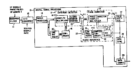
A block diagram ~or one embodiment of the
DPSK demodulation and decoding technique is
illustrated in Figure 7. IF signals having phase
pulses of length T enter bandpass filter 11. Samples
of the band-limited, down-converted MLS waveform are
taken through A/D converter 12 into digital signal
- processor 13. Within digital signal processor 13,
~ these samples are decomposed in Rader processor 14
;; into in-phase and quadrature components. The
algorithms utilized in Rader processor 14 are
discussed in ~A Simple Method for Sampling In-Phase
and Quadrature Components~, Rader, C.M., IEEE
Transactions on Aerospace and Electronic Systems,
Vol. AES-20, No. 6, November 1984, as disclosed
- 25 earlier. These components are treated as a single
sample of the comple~ baseband envelope of the
-~ received MLS waveform.
The series of comple~ samples is delayed by
one bit delay 15 for e~actly one DPSR bit time and
flows through the comples conjugate operation 16.
The coherent detector 17 with its comple~ multiplier
18 and its sliding window average 19 takes the
comple~ conjugate of the delayed sequence and
multiplies it by the undelayed sequence. The signal
is then low pass filtered by averaging together all
samples i~ the p~evious bit period. This sveragi~g
,, ,
WO92/019~ ~ 5 o PCT/US91/03216
-12-
process is known as the sliding window average. This
series of operations results in a sequence of complex
values whose phase angles are a measure o~ the phase
diff2rence between two consecutive DPS~ bits.
Due to the fundamental uncertanties in the
MLS IF ~re~uency, the resultant series of comple~
values may have any phase angle. All values
corresponding to consecutive bits which are in-phase
will have nearly the same angle ~l- All values
corresponding to consecutive bits which are out of
phase will likewise have a common value ~2~ where ~l
~ ~2 - 180.
The series of comples values out of coherent
detector 17 then enters a phase reference calculator
20 where the values are filtered through a low-pass
-~ filter 21 to smooth effects of measurement noise.
During the 13 bit carrier acquisition period of each
; 20 MLS preamble, the comple~ output of low pass filter
2l establishes a "reference~ estimate, r(t), which
e~plicitly defines the in-phase angle of ~l- The
comple~ output then enters the comples conjugate 22
and the comples conjugate of the low pass filter
output, r (t), enters the reference latch 23. The
latched value is used as a reference vector for the
. phase corrector 24 which includes a phase correction
comples multiplier 25 which rotates the phase
detector output onto the real a~is. Following this
rotation, as shown in Figure 8, all binary 0 values
35 will lie on or very near to the positive real a~is
- 36, while all binary l values 35 will lie on or very
near to the negative real axis 37. Since the result
of the comple~ multiplier 25 is on, or very near, the
- 35
.
W() 92/0194X ,~ O ~ O PCr/l S91/03216
--13--
real a~is, only the real part need be used ~or
further processing.
Figure 8a illustrates the input signal, s(t)
31, in polar form as a rotating vector of length v
and angular frequency w. The comple~ output of the
coherent detector, VC(t) 32 is shown in Figure 8b as
either of two fi~ed vectors with magnitude v2 and
fi~ed phase of either wT or wT ~ ~, depending on ~he
encoded information. Note that vc(t) 32 is no longer
rotating. As illustrated in Figure 8c, the reference
signal, r(t) 33, is established during the 832 usec
period of unmodulated carrier, therefore it has a
phase angle of wT. Its conjugate r*(t) is also
illustrated. Finally, Figure 8d illustrates the
result of using r~(t) to correct vc(t). When the
information is a binary zero, bC(t) 35 lies on or
-~- near the positive real a~is 36. When the information
: is a binary 1, bC(t) 35 lies on or near the negative
real a~is 37.
.... .
Note that the actual phase of the comple~
siqnal is never computed directly. All of the
processing from the Rader decomposition through the
carrier tracking filter is performed on the comple~
values and therefore requires only multiplication and
addition operations which can be performed at high
speed in a microcomputer or in dedicated arithmetic
hardware. There are no divisions or inverse
trigonometric functions to be computed, thereby
allowing the technique to be applied to higher data
rates.
Returning to Figure 7, the real result o~
the final phase rotation of the phase corrector 24 is
applied to a pulse width discriminator 27, which is
', ' ' ' ~ ~ ; :
~' , .
WO92/01948 PCT/USgl/03216
2 ~8 6~ -14~
set to identify the presence of the 13-bit carrier
acquisition signal. When the presence o~ this
carrier acquisition signal is detected, the referenc~
signal, r(t), is fi~ed for the duration of the MLS
transmission.
Following the pulse width function
discriminator 27 the real result flows through a data
sync 28 which applies algorithms to detect the
characteristic Barker code and establish bit
synchronization. The result than flows through a
data sample 29 which applies algorithms which sample
the result to establish binary information in
accordance with the signal format and parity
constraints defined in Anne~ 10 to the Convention on
International Civil Aviation; Volume l, Chapter 3.11,
lCAO, Montreal, October l9a7.
To further describe the input signal, we can
utilize typical MLS receiver architecture as
-~ illustrated in Figure 9, where the C-band MLS signal,
including data and scanning beam transmissions, is
down-con~erted and amplified from the 5 GHz range to
. a convenient IF frequency. In the process, a single
MLS channel is selected by filtering the IF signal
through a bandpass filter. The bandwidth of this
filter is chosen to allow for worst case combinations
of ground frequency drift, aircraft doppler, and MLS
receiver local oscillator drift. The shape of this
filter is chosen to accommodate the 300 kHz channel
spacing re~uired in Anne~ 10 to the Convention on
International Civil Aviation; Volume 1, Chapter 3.11,
ICAO, Montreal, October 1987 and the adjacent channel
rejection requirements stated in ~inimum Operational
Performance Standards for Microwave Landina System
Airborne Receivina Eauioment, DO-177, Change 2, RTCA,
~, .
w~ 92/01948 ~ 0 3 u ~ 5 0 PC~/US9i/03216
Washington, D.C., September 1986. The effect of this
filter is to band-limit the MLS signal. Typical MLS
receiver designs have chosen multiple pole filters
with an IF bandwidth o~ 100-150 kHz to satisfy these
requirements.
It is important to note that the
requirements on MLS receiver bandwidth are primarily
driven by frequency source stability and not the
actual information bandwidth of the MLS signal, which
is appro~imately equal to the DPSK data rate, 15.625
kHz.
When the input signal enters the digital
signal processor 13 of Figure 7, it is processed by
Rader processor 14. ~A Simple Method for Sampling
; In-Phase and Quadrature Components", Rader, C.M.,
IEEE Transactions on Aerospace and Electronic
Systems, Vol AES-20, No. 6, November 1984 describes a
technique for decomposing an IF signal into its
constituent in-phase (I) and quadrature (Q)
components using a combination of a rapid sample
rate, relatively low IF frequency, and digital
filtering techniques. As described by Rader, if the
total bandwidth of the signal is B Hertz, the desired
IF frequency is B Hertz, and the desired sample rate
is 4B samples per second. The output of the Rader
processor 13 is a stream of I and Q samples, each
occurring at a rate B, describing the comple~
baseband envelope of the IF wavefor-~. Figure 10
illustrates an implementation of the Rader
technique. As is illustrated in Figure 10, the IF
signal enters bandpass filter 41 and then flows to
A/D c~n~erter 42. The signal then ente~s Rader
:
,~
- . ... .
wo g2/01948 2 0 8 ~ PCT/~S91/03216
-16-
processor 43 where the IF signal is decomposed into
its in-phase (I) 44 and quadrature (Q) 45 componentS-
:
Applying the Rader processor 43 to a signal
; band-limited by an MLS IF filter described in the
previous paragraph would indicate a sample rate of
400-600 kHz (2.5 - l.66 usec spacing), and a minimum
IF frequency of lO0-lS0 kHz. These sample rates and
IF frequencies result in a near-perfect
representation of the complex baseband envelope of
the entire 100-150 kHz MLS bandwidth, which as noted
earlier, is si~ to ten times greater than the
information bandwidth of the MLS DPSK channel.
.
:.- 15 The Rader processor 43 relies on the 4:l
relationship of the input and output sample rates to
simplify the implementation of filters Hl(z) 96 and
H2(z) 47. The technique works with virtually no
- degradation even when the actual sample rate and IF
` 20 frequency vary slightly from the 4:1 relationship.
- For the purposes of demodulating the MLS DPSX, it is
e~tremely desirable to have an integer number of
samples occur in a single DPSX bit period of 64
- usec. Thus, a preferred sample rate is 500 kHz
: 25 providing 2 usec sample spacing and 32 samples per
DPSK bit. A sample rate of 250 kHz or below is
- unacceptable, since it will lead to aliasing of the
IF frequency and will disrupt the I and Q
relationship of the Rader processor 43 outputs.
A key feature of the Rader processor 43 is
that the net filter transfer function H(z) is
comple~, consisting of Hl(z) + jH2(z). Thus the H(z)
filter is unrealizable in a physical sense without
decomposition into I and Q channels via a power
divider, quadrature misers, etc. This approach of
W~92/01948 2 0 8 ~ ~ ~ O PCT/US91/03216
-17-
processing the comDlex envelope of the signal is
carried throughout the remaining DPSK demodulation
process.
Following the Rader processor decomposition,
we are left with I and Q samples spaced 8 usec
apart. In the event that the mathematical operations
described ne~t can not be accomplished in this
period, acceptable perEormance may be obtained by
further down-sampling this comple~ envelope to 16
usec, 3Z usec or even 64 usec intervals. The minimum
sample rate of 15,625 comple~ samples per second
still satisfies all Nyquist requirements for the
15.625 kHz MLS bit rate. Such down-sampling may
cause aliasing of any error frequency E and will
reduce noise performance by eliminating the
possibility for filtering the phase detector output.
Aliasing of the error frequency E will not, in
itself, affect the succeeding processing.
The coherent detection process of the
coherent detector 17 of Figure 7 involves a
straightforward comple~ multiplication in rectangular
form. This process involves only multiplication and
addition operations, and can thus be efficiently
implemented in ~ither hardware or software. With a
comple~ input signal s(t) from the Rader processor 14
- we have the following.
(g) s(t)- sI(t) + jsQ(t)
(lO) v(t), s(t)s (t-T)
. [sI(t)sI(t-T)+sQ(t)sQ(t-T)]
+ j[-sI(t)sQ(t-T)+sQ(t)sI(t-T)]
. .,
.
WO92/019~ 2 0 '~ PCT/US91/03216
-~8-
The coherent deteotor output is this resul~
filtered by the sliding window average l9 having a
duration equal to the DPS~ bit width of 64 usec.
Assuming the nominal 8 usec period between samples (~
. 8 usec), there are eight-samples within the sliding
window.
(ll) vc(t) ~ (l/8) ~v(t-n~)
n.o
This filtering process requires only
additions and a 3 place binary shift to divide by
eight.
The phase reference computation as performed
by the phase reference 20 will now be described.
During the 13 bit carrier acquisition period, the
comple~ synchonous detector output vc(t) given by
equation (ll) is essentially constant. This comple~
value is first low pass filtered by low pass filter
21 to establish the reference phase signal r(t).
Although the filter implementation is up to the
designer, a single pole recursive filter has
demonstrated adequate performance.
(12) r(t) ~ Ar(t-~) + (l-A)vc(t)
where ~ is the net sample rate, nominally 8 usec.
The signal then flows to the phase corrector
24 where the comple~ value r(t) is used as an
estimate of the unknown zero-degree phase~ vector,
including any effects of IF frequency errors. A
WO92/019~ 2 0 8 o ' ~ O PCT/US91/0321b
-19-
corrected signal bR(t) is created in accor~ance with
equation (8), using the rectangular form o~ r(t)
(13) bR(t) ~ VcI(t)rI(t) + VCQ(t)rQ(t)
Once again, this process is implemented in either
hardware or software with only a simple multiply and
accumulate function. Some intermediate scaling of
the multiplicands may be necessary to prevent
overflow of the result bR(t).
The real output bR(t) is an integer value
whose algebraic sign represents the encoded binary
information. After the Rader processor 14, sliding
window average 19, and low pass filters 21 have
settled down, this value will remain positive for the
remainder of the 13 bit acquisition period. The
pulse width discriminator 27 checks the sign of
bR(t), and enables further processing when the signal
is positive for longer than a fi~ed period of time.
In the preferred MLS embodiment, this period is set
to 640 usec, or l0 DPSR bits.
The pulse width discriminator 27 involves a
digital comparator 5l and a binary down counter 52,
as shown in Figure ll, and can be implemented in
either hardware or software, as appropriate to the
intended application.
The output of the pulse width discriminator
27 is low until a valid pulsewidth is detected. Upon
detection the output transitions immediately to a
high condition, and remains high until reset at the
- end of the MLS function. The low-to-high transition
causes two actions to occur:
W092/01~4X PCT/US91/03216
~8 ~50 -20-
(l) the comple~ re~erence value r~tpwd) at
the transition time, tpwd, is latched and used for
the remainder o~ the DPSK func:tion;
t2) the real BPS~ video output, consisting
of a sequence of digital words representing bR~t) is
gated to the synchronization and data sampling
algorithms, discussed below.
The data sync 28 will now be described. The
MLS signal format utilizes a five bit Barker Code
(binary data lll0l) for receiver time
synchronization. This code is transmitted
immediately following the 13 bit acquisition period.
The receiver reference time is defined as the
midpoint of the final phase transition.
This reference time is ideally recovered by
use of a matched filter to correlate the received
BPSK video signal bR(t) against a Barker Code
template, BC(t). To ensure proper operation, BC(t)
must be sampled at the same rate as bR(t), thus, for
the 8 usec sample rate used in this discussion, the
Barker Code Template, BC is shown in Figure 12. Use
of a matched filter approach will result in the best
appro~imation of the true reference time.
Time constraints on the real time processing
may make the ideal matched filter impractical to
implement. Sub-optimal methods of attaining
synchronization are acceptable in the MLS
application. One such technique which has been shown
to provide acceptable MGS performdnce is the
"zero-crossing-reset" method which is illustrated in
Figure 13, and discussed below..
WO92/01948 ~ iJ V ~ U PCT/US91/03216
--21-
Once the pulse width discriminator 27 o~
Figure 7 has indicated that a ~alid candidate signal
is present, successive values of bR(t) are examined
until the ~irst sign crossing takes place. In a
perfect M~S signal, as illustrated in Figure 14, this
should occur at the end of the 13th acquisition bit,
which is a logical "0" and the start of the first
Barker Code "l". If there are N samples per DPSK bit
(N.8 for 8 usec samples), the sign of the (N/Z)th
value of bR(t) after the sign transition is e~amined,
and the appropriate BPSK binary value (no" or "l") is
entered into a five bit shift register. This process
is repeated every Nth sample after this first entry
until either another sign change is detected or ten
l; bits are sampled.
If another sign change is detected between
samples of the BPSR binary value, the succeeding BPSR
sample is taken (N/2) samples after the transition,
this process is repeated every Nth sample after the
new BPSR sample until either another sign change is
detected or a total of ten bits are sampled.
:,
As each new 8PSR sample is shifted into the
shift register, the register contents are compared to
the Barker Code template of lll0l. If a Barker Code
match occurs, the interpolated zero crossing between
the two samples bracketing the previous sign changes
is accepted as the reference time. This
- 30 interpolation process may require a -icroprocessor,
although all other steps are effectively implemented
directly in hardware.
If no Barker Code match occurs after l0 B~SR
data samples, the entire demodulation process,
: .
WO92/01948 2 0 8 ~ ~ ~ PCT/US91/03216
-22-. -
including the pulse width discriminator and all
filter memories, is reset and restarted.
The data sampling process performed in data
sample 29 of Figure 7 is described as follows. Once
the Barker Code has been identi~ied, the sign o~
every Nth ~PSX video value is esamined to arrive at
the proper BPSR data. Positive BPSX video values are
logical BPS~ "0~ values. Negative BPSK video values
are logical BPSR ~ values. At this point,
conventional data decoding, parity checking and data
validation algorithms may be used.
A block diagram of a preerred embodiment of
the present invention is illustrated in Figure lS.
In this embodiment, the high-speed capabilities of
the TMS-320C25 digital signal processor chip 61 with
: its ROM 62, RAM 63 and oscillator 64 are utilized to
implement the entire process just described in
software. Support logic includes a 12-bit
analog-to-digital converter 65 and its associated
timing and control circuitry 66. The interface to
the digital signal processor chip 61 is through a
FIFO 67. The counter 68 is used to count a fi~ed
number of data samples ~either 4 or 8) collected in
the FIFO 67 before digital signal processor interrupt
request are issued.
A block diagram of a more generalized
embodiment of the present invention is shown in
Figure 16. This embodiment is based on the same
~ general purpose hardware-digital signal processor
.~ architecture illustrated in U.S. Patent No. 4,926,186
by Kelly and LaBerge and assigned to the same
assignee as the present invention. This architecture
uses one of several commercially available multiply
WO92/01948 2 0 8 ~ ~ ~ O PCT/US91/03216
-23-
and accumulator (MAC) chips 71 under microcode
control from the microcoded controller 72 to per~orm
the various arithmetic operations described earlier
at a significantly higher speed than that currently
available in a software controlled digital signal
processor chip. Also illustrated in Figure 16 is
microprocessor 73, pulse width discriminator 74,
sample counter 75 and A/D Converter 76 with its
timing and control circuitry 77. Increasing the
computation speed, allows use of a higher A/D clock
rate and correspondingly higher IF frequency and
signal bandwidth. This implementation may be
attractive when adopting the present invention to
non-MLS applications.
Although the present invention was developed
specifically for an MLS application, it may be
applicable to any DPSK demodulation application,
providing an MLS-like carrier acquisition period is
available.
It is not intended that this invention be
limited to the hardware or software arrangement, or
operational procedures shown disclosed. This
invention includes all of the alterations and
variations the~eto as encompassed within the scope of
the claims as follows.
3i