Note: Descriptions are shown in the official language in which they were submitted.
_1_
ADAPTIVE EQUALIZER AND RECEIVER
R~rKr_RnrTUn nF THR TNVFNTInN
1. Field of..the Invention
The present invention relates to an adaptive
equalizer which is used for minimizing degradation of
transmission characteristics in high bit rate digital mobile
communication, in which transmission characteristics are
substantially degraded by waveform distortion due to
frequency selective fading. The present invention also
relates to a receiver which may be used in an environment
attended with frequency selective fading.
2. Description of the Prior Art
There have heretofore been baseband waveform adaptive
equalizers which are capable of tracking a rapid time-
varying channel as in mobile communication and whose initial
setting can be effected by a training process in a short
period of time. One example of known adaptive equalizers
of the type described above is a decision-feedback adaptive
equalizer which is disclosed in Nakajima and Sampei,
"Performance of a Decision Feedback Equalizer under
Frequency Selective Fading in Land Mobile Communications",
the Transaction of the Institute of Electronics, Information
and Communication Engineers (B-II), J72-B-II, No. 10,
pp.513-523 (October 1989).
Fig. 42 is a block diagram of the decision-feedback
adaptive equalizer disclosed in the above-mentioned
literature, which is designed for a system in which the
received signal is a QPSK modulation signal (transmission
bit rate: 2/T bps; T is 1 symbol time).
In the figure, reference numeral 1 denotes a
feedforward transversal filter (hereinafter referred to
as "FF part") in which the tap interval is a predetermined
delay time Tp (second) and the number of taps is L, and 2
a feedback transversal filter (hereinafter referred to as
"FB part") in which the tap interval is a predetermined
delay time T (second) and the number of taps is (M-L).
An adder 3 adds together data output from the FF and FB
parts 1 and 2. A decision circuit 4 identifies a data
-2-
sequence output from the adder 3 every T sec. and makes
a hard decision thereon. A tap-coefficient-update circuit 5
determines tap-coefficients for the FF part 1 and the FB
part 2 every T sec. A switching circuit 6 functions such
that either the output data sequence of the decision circuit
4 or a reference data sequence is selectively input to the
FB part 2. Reference numeral 7 denotes a received signal
input port of..the decision-feedback adaptive equalizer, 8
a reference sequence input port, and 9 an output port of
the adaptive equalizer.
Fig. 43 shows one example of burst format for signals
employed in mobile communication.
The burst shown in Fig. 43 comprises a unique word
(U~Y) 13 which is used for training of a decision-feedback
adaptive equalizer and for establishing frame
synchronization, random data a (information bits) 14,
a color code (hereinafter referred to as "CC") 15 which
is used for identification of a base station or as
a training sequence for the equalizer, and random data b
(information bits) 16.
The operation of the conventional decision-feedback
adaptive equalizer will be explained below.
In the decision-feedback adaptive equalizer shown
in Fig. 42, which is designed for a system in which the
received signal is a QPSK modulation signal, the received
signal is converted into a baseband signal by a demodulator,
and channel characteristics are estimated by using the UW 13
(shown in Fig. 43), which is at the head of each burst, thus
effecting convergence of the tap-coefficients (training
mode). The signal input to the FB part 2 at this time is
data without decision error, that is, a reference data
sequence that is determined by the UW 13. Next, equalization
is executed on the random data a 14, the CC 15 and the random
data b 16 (tracking mode).
For the random data a 14 and the random data b 16,
the signal output from the decision circuit 4 is input to
the FB part 2 as a received signal sequence. For the CC 15,
_. -3-
a reference data sequence that is determined by the CC 15 is
input to the FB part 2.
The tap-coefficient-update circuit 5 updates the tap
coefficients of the FF and FB parts 1 and 2 for each symbol
according to a tap-coefficient-update algorithm, e.g.,
Kalman filter algorithm (RLS algorithm), by using the
received signal sequence input to the decision-feedback
adaptive equalizer, reference data sequences that are
determined by the respective known training sequences of
the UW 13 and the CC 15, the output data sequence of the
decision circuit 4, and the output data from the adder 3.
As one example of the tap-coefficient-update
algorithm, Kalman filter algorithm (RLS algorithm) will
be briefly explained below.
It is assumed that the signal vector input to the
equalizer at time t=nT (n=0,1,2,...) is XM(n), the tap-
coefficient is CM(n), the equalizer output is I(n), the
desired output is d(n), and the error is e(n).
Here, XM(n),. CM(n), I(n) and d(n) are complex numbers
comprising in-phase and quadrature channels.
Assuming that the number of taps in the FF part 1 of
the decision feedback adaptive equalizer is L and the total
number of taps is M, the above factors are represented as
follows
XM(n)=(Y1~(n),Y2~(n)~...,yL~(n)~
dl~(n)~d2~(n)~...,dM-L~(n)]~ (1)
CM(n)=~C1~(n)~C2~(n),...,CM~(n)] (2)
I(n) - CM~(n-1)XM(n) (3)
e(n/n-1)=d(n)-I(n)=d(n)-CM~(n-1)XM(n) (4)
In the above equations ~ represents a complex
conjugate transpose matrix (or vector).
In addition, d(n) is a known training sequence in
the training mode, whereas in the tracking mode it is
an output data sequence obtained from the decision circuit 4
as a result of a hard decision made on the result of
-4-
Equation 3. The desired value in this algorithm is the tap-
coefficient CM(n) which minimizes the estimation function E
represented by
n
_~ ~n-i e~,(i/n)e(i/n) (5)
i=1
where ~ represents the forgetting factor (0<~sl).
CM(n) that minimizes Equation 5 is given by
CM(n)=R 1(n)D(n) (6)
_ n _
P 1(n)=R(n)= ~ ~n 1XM(i)Xy~~(i)+B~nI (7)
i=1
where ~ represents a positive constant.
n _
D(n)=~ ~,n 1XM(i)d*(i) (8)
i=1
The algorithm for recursively obtaining CM(n) at time
t=nT from CM(n-1) and P(n-1) at time t=(n-1)T is as follows:
K(n)=P(n-1)XM(n)/[a+XM*(n)P(n-1)XM(n)7 (9)
P(n)=[P(n-1)-K(n)XM*(n)P(n-1)J (10)
CM(n)=CM(n-1)+K(n)e~(n/n-1) (11)
P(0)=a 1I, CM(0)=0 (12)
where K(n) is the Kalman gain, P(n) the tap-
coefficient error covariance matrix, and I the identity
matrix.
It should be noted that the tap-coefficient-update
algorithm is described in detail in S. Haykin, "Introduction
to Adaptive Filters", Chapter 5, Gendai Kogaku-Sha (1987),
translated by Tsuyoshi Takebe, and J.G. Proakis, "Digital
Communications", Chapter 6.8, McGraw-Hill (1983).
In the foregoing, the decision-feedback adaptive
equalizer, which is designed for a system in which the
received signal is a- QPSK modulation signal, as shown in
Fig.-42, has been described; the following is consideration
of a case where the received signal input to the above-
described adaptive equalizer is a 1I/4 shifted QPSK modulation
signal (transmission bit rate: 2/T bps; T is symbol time).
__.
Here, as one example of 1I/4 shifted QPSK modulation,
an encoding scheme that is disclosed in EIA Document, IS-54,
"Cellular System Dual-Mode Mobile Station Compatibility
Standard" (Dec. 1990) will be shown, and the reference
signal of the adaptive equalizer for the encoding scheme
will also be explained.
Fig. 44 is a block diagram showing one example of
a means for encoding a transmission data sequence according
to the above encoding scheme.
Referring to Fig. 44, a transmission data sequence bm
is converted sequentially from the first data by serial-to-
parallel conversion in such a manner that odd-numbered data
is converted into a data sequence XK, while even-numbered
data is converted into a data sequence YK. Then, (XK,YK)
is converted into a transmission data sequence (IK,QK) by
differential encoding according to Equations 13a and 13b:
IK=IK-lcos[~~(XK,YK)~
-QK-lsin[o~5(XK,YK)7 (13a)
QK=IK-lsin[A~(XK,YK)~
+QK-lcos[~~(XK,YK)l (13b)
The phase change o~ is given according to the table
shown in Fig. 45.
Assuming that the reference point (I1,Q1) is (21/2,0)
and that the transmission data sequence bm (1,-l,l,-1,1,-1,
-1,1,-1,-1,-1,1,1,1,-1,1,1,1,1,-l,-1,1,-1,-1,1,-l,l,-1) is
processed according to the above encoding scheme, it is
converted into a differentially encoded data sequence
(IK,QK) shown in the table of Fig. 46.
Accordingly, when the transmission data sequence bm
is the UW 13 or the CC 15, the data sequence (IK,QK) shown
in the table of Fig. 46 is used as a reference data sequence
for the adaptive equalizer shown in Fig. 42.
Next, the decision circuit of the conventional
adaptive equalizer will be explained.
In the decision-feedback adaptive equalizer shown in
Fig. 42, a decision is made on the output of the adder 3 in
the decision circuit 4 by using a method explained below:
-6-
First, the output (II(K),Ie(K)) of the adder 3 (K
represents the output data of the adder 3 for the K-th
symbol) is sorted according to whether K is an odd number
or an even number.
(a) When K is an odd number: the output (II(K),IQ(K)) of
the adder 3 is subjected to an arithmetic operation for 1I/4
phase rotation, and the phase-rotated data (II~(K),IQ~(K))
is judged to determine a decision value (dI(K),dQ(K))
according to whether the sign of (IIr(K),IQ~(K)) is positive
or negative, as shown in Fig. 47(a).
(b) When K is an even number: the output (II(K),IQ(K)) of
the adder 3 is judged to determine a decision value
(dI(K),de(K)) according to whether the sign of (II(K),IQ(K))
is positive or negative, as shown in Fig. 47(b).
Further, the above decision value (i.e., the output
of the decision circuit 4) is differentially decoded to
obtain an equalized data sequence.
As has been described above, when the received signal
input to the adaptive equalizer shown in Fig. 42 is a 1I/4
shifted QPSK modulation signal, the output (II(K),IQ(K)) of
the adder 3 is sorted according to whether K is an odd
number or an even number. When K is an odd number, the
output (II(K),Ie(K)) of the adder 3 needs an arithmetic
operation for lI/4 phase rotation. Therefore, the number
of arithmetic operations required in the decision circuit 4
increases, and the arrangement becomes complicated.
In the meantime, conventional receivers used in time-
division multiplex (TDM) or time-division multiple access
(TDMA) communication include the one that is disclosed in
Yamamoto and Kato, "TDMA Communications", the Institute of
Electronics, Information and Communication Engineers (1989),
for example.
Fig. 48 is a block diagram of a demodulator part
including a frame synchronization system in the conventional
receiver, disclosed in the above-mentioned literature.
In the figure, reference numeral 101 denotes an
input port for a received IF signal. A demodulator 102
extracts a timing clock and data from the received IF
..._ -7-
signal and outputs them. A UW detector 103 performs UW
detection on the basis of the data output from the
demodulator 102 and outputs either a UW detection signal
or a UW missed detection signal. A frame synchronization
control circuit 104 effects frame synchronization control on
receipt of the UW detection signal.
Fig. 49 is a block diagram showing exemplarily
the internal arrangement of the UW detector 103 shown in
Fig. 48.
In the figure, reference numerals 121 and 122 denote
input ports for data of two quadrature channels Ich and Qch
output from the demodulator 102, and 123 an input port for
a recovered clock output from the demodulator 102. A
correlator 124 receives the Ich data as an input signal
and operates on the basis of the recovered clock supplied
through the input port 123, while a correlator 125 receives
the Qch data as an input signal and operates on the basis of
the recovered clock supplied through the input port 123. An
adder 126 adds together the outputs of the two correlators
124 and 125. A comparator 127 makes a comparison between
the output of the adder 126 and a predetermined threshold
and outputs a UW detection signal in accordance with the
result of the comparison. Reference numeral 128 denotes
an output port of the comparator 127.
Fig. 50 is a block diagram showing exemplarily the
internal arrangement of the correlator 124 shown in Fig. 49.
In the figure, a correlator input port 130 is
equivalent to the input port 121 of the UW detector 103.
Reference numeral 131 denotes an input port for
the recovered clock. A shift register 132 has a number
of stages corresponding to the UW length (unit symbol) for
taking in the input signal and operates on the basis of
the recovered clock. A register 133 has a number of stages
corresponding to the UW length (unit symbol) for storing
the Ich UW pattern. A multiplexer part 134 comprises
multiplexers which are each arranged to multiply together
a pair of corresponding bits of data stored in the shift
register 132 and the register 133. An adder 135 adds
_8_ ~g ~~ ~
together the outputs of the multiplexers constituting the
multiplexer part 134. Reference numeral 136 denotes
an output port of the adder 135.
It should be noted that the correlator 125 is
arranged in the same way as the correlator 124 except that
the register 133 in the correlator 125 stores the Qch UW
pattern.
The operation of the UW detector 103 will be
explained below with reference to Figs. 48, 49 and 50.
In the correlator 124, the Ich data in the output of
the demodulator 102 is input to the shift register 132, and
the contents of the shift register 132 are shifted to the
right in response to the recovered clock. Bits of data
which are shifted to the right in the shift register 132
are multiplied in the respective multiplexers by the
corresponding bits of the known Ich UW pattern (rl to r~)
stored in the register 133, and the resulting outputs bf
the multiplexers are input to the adder 135. The adder 135
adds together the outputs of the multiplexers and outputs
a correlation value between the data stored in the shift
register 132 and the register 133.
Similarly, the correlator 125 determines a
correlation between the Qch data and the known Qch UW
pattern and outputs a correlation value.
The respective outputs of the correlators 124 and 125
are added together in the adder 126. As a result, the total
correlation value between the input data and the Ich and Qch
UW patterns is input to the comparator 127.
The comparator 127 makes a comparison between the
output value of the adder 126 and a predetermined threshold
A. When the adder output value z A, the comparator 127
sends a UW detection signal to the frame synchronization
control circuit 104, whereas, when the adder output value
c A, the comparator 127 sends a UW missed detection signal
to thewcircuit 104. On receipt of the UW detection signal
or the UW missed detection signal, the frame synchronization
control circuit 104 recognizes the frame position and the
... - g -
synchronization state and then effects frame synchronization
control.
It should be noted that the UW detector is detailed
in the above-mentioned literature "TDMA communications",
pp.48.
In mobile communication where frequency selective
fading is present in the channel, however, the conventional
receiver arrangement shown in Fig. 48 suffers from
degradation of the transmission characteristics, and
there is therefore a demand for a receiver equipped with
an adaptive equalizer as one of the measures to solve the
problem.
The conventional adaptive equalizers, arranged as
described above, suffer from problems as stated below:
When the received signal is a 1I/4 shifted QPSK
modulation signal, the decision circuit of the adaptive
equalizer needs to sort the output of the adder when making
a decision and to execute an arithmetic operation for 1I/4
phase rotation, so~that the number of arithmetic operations
required in the decision circuit increases, resulting in
a complicated arrangement.
In addition, if data decision errors occur
successively due to rapid time-varying channel
characteristics after the tap-coefficients have been made
to converge to the optimum values by estimating the channel
characteristics by use of the UW at the head of a burst
in the presence of frequency selective fading, updating
of the tap-coefficients cannot be effected in the direction
in which the tap-coefficients converge to the optimum
values, so that the bit error rate for data in the latter
half of the burst increases.
In addition, since the bit error rate remains high
until the tap-coefficients are made to converge to the
optimum values by estimating channel characteristics by
use of the UW at the head of a burst in the presence of
frequency selective fading, the UW detection probability
at the UW detector that uses the output of the decision
circuit in the adaptive equalizer is low.
... _lo_
In addition, when the received signal input to the
adaptive equalizer has a frequency offset due to the
difference between the carrier frequency of the received
signal and the local oscillator frequency of the receiver
including the adaptive equalizer, equalization cannot be
performed in such a manner as to follow up the phase change
of the received signal caused by the frequency offset, so
that the equalization characteristics degrade considerably.
The conventional receiver having the above-described
arrangement suffers from the following problems.
To obtain synchronization for reception as a
synchronization control procedure in the conventional
receiver, a UW detection signal is obtained from data output
from the demodulator, thereby effecting synchronization
control.
However, if an adaptive equalizer is provided in
the demodulator to cope with the fast variation of channel
characteristics in the presence of frequency selective
fading, it is necessary to know the UW position at the head
of the burst in advance (that is, frame synchronization must
be established in advance). However, since the UW position
has not yet been known at the time of initial acquisition
or hand off, the adaptive equalizer cannot operate, so that
the receiver cannot start on its operation (that is, frame
synchronization cannot be attained).
In addition, when a demodulator including an
equalizer is used in the presence of frequency selective
fading, it may be impossible to detect the UW position
accurately because the output value of an incoherent
correlator included in the demodulator depends on not
only the input data pattern but also other factors due
to rapid level variation caused by the fading.
In addition, when a demodulator including an adaptive
equalizer is used, the adaptive equalizer cannot operate due
to a frequency offset of the received signal at the time of
initial acquisition or hand off, so that the UW position
cannot be detected in the UW detector and hence frame
synchronization control cannot be effected.
SUMMARY OF THE INVENTION: 11-
In view of the above-described circumstances, it is
an object of the invention of Claim 1 to provide an adaptive
equalizer which is designed so that the decision circuit
that makes a decision on a received signal of 1I/4 shifted
QPSK modulation has a simplified arrangement.
It is an object of the invention of Claims 2 and 3
to provide an adaptive equalizer which is designed so that
even in a case where channel characteristics vary rapidly
in the presence of frequency selective fading, the bit error
rate in the latter half of each burst is minimized, thereby
reducing the bit error rate in the burst as a whole.
It is an object of the invention of Claim 4 to
provide an adaptive equalizer which is designed so that the
UW detection probability in the presence of frequency
selective fading is increased.
It is an object of the invention of Claims 5 and 6
to provide an adaptive equalizer which is designed so that
even if the received signal has a frequency offset, the
degradation of the equalization characteristics due to the
frequency offset is minimized.
It is an object of the invention of Claim 7 to
provide a receiver wherein the UW position is detected
before frame synchronization is established, thereby
enabling frame synchronization control to be effected
even at the time of initial acquisition or hand off in
the presence of frequency selective fading.
It is an object of the invention of Claim 8 to
provide a receiver which is designed so that even when
there is rapid level variation in the presence of frequency
selective fading, UW detection can be performed normally and
frame synchronization control can be effected normally.
It is an object of the invention of Claims 9, 10 and
11 to provide a receiver which is designed so that even when
there is a frequency offset due to the difference between
the carrier frequency of the received signal and the local
oscillator frequency of the receiver including an adaptive
equalizer at the time of initial acquisition or hand off, U«'
-12- ~~~t~
detection can be performed normally and frame
synchronization control can be effected normally.
To attain the above-described objects, the invention
of Claim 1 provides an adaptive equalizer having
a transversal filter, a decision part, and a tap-
coefficient-update part that updates tap-coefficients
of the transversal filter according to a tap-coefficient-
update algorithm, e.g., Kalman filter, wherein the
improvement is characterized by comprising a complex
multiplexer that phase-rotates a received signal input
to the transversal filter, and a differential decoder
that differentially decodes the output of the decision
part, and in that the received signal is equalized after
a (lI/4) phase rotation component has been eliminated
therefrom.
In addition, the invention of Claim 2 provides
an adaptive equalizer having a transversal filter,
a decision part, and a tap-coefficient-update part that
updates tap-coefficients of the transversal filter according
to a tap-coefficient-update algorithm, e.g., Kalman filter,
wherein the improvement comprises: means for initializing
the tap-coefficient-update part and the tap-coefficients
of the transversal filter a plurality of times during one
burst; and means for retraining the transversal filter by
using a training sequence contained in the burst.
In addition, the invention of Claim 3 provides
an adaptive equalizer as defined in Claim 2, which further
comprises means for making a comparison between a training
sequence interposed in the burst, which has been equalized,
and a known training sequence; and means for initializing
the tap-coefficients and executing retraining only when
there is an error in the equalized training sequence.
In addition, the invention of Claim 4 provides
an adaptive equalizer having a transversal filter,
a decision part, and a tap-coefficient-update part that
updates tap-coefficients of the transversal filter according
to a tap-coefficient-update algorithm, e.g., Kalman filter,
wherein the improvement comprises: a memory for storing
-13-
a received signal; and a unique word (hereinafter referred
to as "UW") detector that effects UW detection by using
the inner product of the last updated tap-coefficients
for the UW and the received signal stored in the memory.
In addition, the invention of Claim 5 provides
an adaptive equalizer as defined in Claim 4, which further
comprises: means for subjecting UW data stored in the
memory to an arithmetic operation to provide phase rotations
corresponding to different frequency offsets; UW detection
means that sends the result of the arithmetic operation
to the transversal filter and effects UW detection with
respect to the UW data; and means for estimating a frequency
offset by using the result of the UW detection and for
compensating for the frequency offset.
In addition, the invention of Claim 6 provides
an adaptive equalizer having a transversal filter, a
decision part, and a tap-coefficient-update part that
updates tap-coefficients of the transversal filter according
to a tap-coefficient-update algorithm, e.g., Kalman filter,
wherein the improvement comprises: a memory disposed
in front of the transversal filter to store a received
signal; and means for estimating for each burst a frequency
offset direction by using the last updated tap-coefficients
for the UW and the received signal stored in the memory,
for detecting a frequency offset direction by averaging
the estimated frequency offset directions, and for making
compensation for frequency offset at a certain minute step.
In addition, the invention of Claim 7 provides
a receiver comprising: means for quasi-coherently detecting
a received signal; a memory for temporarily storing received
data output from the quasi-coherent detection means;
an address counter that designates a write address for
the memory; an incoherent correlator.that determines
correlation between a received data pattern output from
the quasi-coherent detection means and a known UW pattern;
means for tentatively detecting a UW position on the basis
of an output of the address counter and an output of the
incoherent correlator; an adaptive equalizer that equalizes
m.. _14_ ~ ~~~3~~i:
the received data in the memory on the basis of an output
of the UW position tentative detection means; a UW detector
that detects a UW position on the basis of the equalized
data; and means for effecting frame synchronization control
on the basis of an output of the UW tentative detection
means and an output of the UW detector.
In addition, the invention of Claim 8 provides
a receiver as defined in Claim 7, further comprising means
for selecting either a hard decision value or a soft
decision value, which are obtained from data output from
the quasi-coherent detection means, as one signal input
to the incoherent correlator.
In addition, the invention of Claim 9 provides
a receiver as defined in Claim 8, which further comprises
means by which when UW data is to be sent to the adaptive
equalizer, coarse AFC is effected in advance by using the
output of the incoherent correlator, and a plurality of UW
data which have been phase-rotated at minute steps around
the frequency attained by the coarse AFC are sent to the
adaptive equalizer to effect UW detection for each UW data.
In addition, the invention of Claim 10 provides
a receiver as defined in Claim 9, which further comprises:
a mixer which effects frequency conversion of a received
signal; a voltage controlled oscillator which gives a local
oscillator output to the mixer; and means for detecting
a frequency offset in the adaptive equalizer and for feeding
it back to the voltage controlled oscillator to make
compensation for frequency offset.
In addition, the invention of Claim 11 provides
a receiver as defined in Claim 10, which further comprises:
means for estimating a frequency offset direction for each
burst in the adaptive equalizer by using the last updated
tap-coefficients for the UW and the received signal stored
in the memory; means for detecting a frequency offset
direction by averaging the estimated frequency offset
directions; and means for making compensation for
a frequency offset when detected by changing the control
... lS ~i~~~
voltage applied to the voltage controlled oscillator
in a direction in which the frequency offset is canceled.
The above-described adaptive equalizers and receivers
according to the present invention function as follows:
In the adaptive equalizer of the invention according
to Claim 1, when a 1I/4 shifted QPSK modulation signal is
received, the 1I/4 phase rotation component is eliminated
from the received signal in the complex multiplexer provided
in the input stage of the adaptive equalizer, thereby
eliminating the need for sorting each output data of the
adder and for an arithmetic operation for 1I/4 phase rotation
in the decision circuit, and thus making it possible to
simplify the arrangement of the decision circuit.
In the adaptive equalizer of the invention according
to Claim 2, when the CC and data following it are to be
equalized, the tap-coefficient-update circuit and the tap-
coefficients are initialized by the initialization circuit,
and retraining is executed with the CC used as a reference
data sequence for reestimation of the channel, thereby
minimizing the increase in the bit error rate in the latter
half of the burst even when there is a large change in the
channel condition during one burst, and thus improving the
bit error rate in the burst as a whole.
In the adaptive equalizer of the invention according
to Claim 3, when the CC and data following it are to be
equalized, a comparison is made between the result of
equalization executed without initializing the tap-
coefficient-update circuit and the tap-coefficients and the
known transmission signal sequence of the CC, and only when
there is an error in the equalized data sequence, the tap-
coefficient-update circuit and the tap-coefficients are
initialized, and retraining is executed to reestimate the
channel, thereby improving the bit error rate in the burst
as a whole.
In the adaptive equalizer of the invention according
to Claim 4, UW detection is effected by making a comparison
between the inner product of the last updated tap-
coefficients for the UW and the received signal read out
.. -16-
from the memory and a known training sequence UW, thereby
making it possible to minimize the lowering of the UW
detection probability even in the presence of frequency
selective fading.
In the adaptive equalizer of the invention according
to Claim S, the received signal is phase-rotated with
different frequency offsets, and UW detection is effected
with respect to the received signal phase-rotated in this
way, so that even if the received signal has a frequency
offset, the UW detection probability increases. In
addition, the frequency offset can be estimated from the
result of UW detection carried out on each of the phase-
rotated received signal data. Therefore, by making
compensation for the frequency offset, the equalization
characteristics are improved.
In the adaptive equalizer of the invention according
to Claim 6, a frequency offset direction of the received
signal is estimated for each burst, and the frequency offset
directions estimated over several bursts are averaged to
detect the frequency offset direction of the received
signal, whereby the estimation accuracy is improved. In
addition, by making compensation for the frequency offset,
the equalization characteristics are improved.
The functions of the receivers of the present
invention according to the respective Claims, which are
arranged as described above, will be explained below.
In the receiver of the invention according to
Claim 7, the UW position is tentatively detected by the
incoherent correlator, and the demodulator is activated
by using the tentatively detected UW position, thereby
enabling the demodulator, including the adaptive equalizer,
to be activated before the frame synchronization control
circuit starts its operation. In addition, it is possible
to realize UW detection of high accuracy by effecting final
UW detection with respect to the output of the demodulator,
which has undergone adaptive equalization.
-17-
In the receiver of the invention according to
Claim 8, when UW detection is performed in a range where
the level variation cannot be ignored, the input signal of
the incoherent correlator is subjected to a hard decision,
thereby enabling the influence of the level variation to
be eliminated, whereas, when UW detection is performed in
a range where the level variation can be ignored, the input
signal of the incoherent correlator is subjected to a soft
decision, thereby allowing the desired operation.
In the receiver of the invention according to
Claim 9, coarse AFC is effected in advance, and a plurality
of UW data which have been phase-rotated with different
frequencies are sent to the adaptive equalizer to effect
UW detection, whereby UW detection of high accuracy can be
performed even when the received signal has a frequency
offset .
In the receiver of the invention according to
Claim 10, a frequency offset that is estimated in the
adaptive equalizer is fed back to the VCO (voltage
controlled oscillator) to make compensation for the
frequency offset, whereby stable demodulation can be
realized even when the received signal has a frequency
offset .
In the receiver of the invention according to
Claim 11, a frequency offset that is estimated in the
adaptive equalizer is fed back to the VCO. In addition,
the frequency offset direction is detected for each burst
in the adaptive equalizer, and the frequency offset
directions thus detected are averaged to detect the
frequency offset direction of the received signal, which
is then fed back to the VCO to make compensation for the
frequency offset, whereby stable demodulation can be
realized even when the received signal has a frequency
offset.
-17a-
Accordingly, in the one aspect, the present
invention provides a method for equalizing an input
signal, comprising the steps of: training a transversal
filter by updating tap-coefficients of the transversal
filter according to an output obtained by applying the
input signal to the transversal filter; applying the
input signal to a feedforward part of the transversal
filter; applying a known training sequence to a feedback
part of the transversal filter; subjecting the output of
the transversal filter to a decision; comparing the
result of the decision to the known training sequence to
obtain an error vector; estimating a frequency offset
direction using the error vector; and compensating for
frequency offset in the input signal using the estimated
frequency offset direction.
In a still further aspect, the present invention
provides a system for equalizing the input signal,
comprising: a transversal filter having an input, an
output, and a plurality of tap-coefficients; means for
training the transversal filter by updating tap-
coefficients on the transversal filter according to an
output obtained by applying the input signal to the
transversal filter; means for estimating a frequency
offset direction of the input signal according to an
average of frequency offset directions estimated for
each burst; and means for compensating for a frequency
offset in the input signal using the estimated frequency
offset.
BRIEF DESCRIPTION OF THE DRAWINGS
The above and other objects, features and
advantages of the present invention will become more
apparent from the following description of the preferred
embodiments thereof,
A
-18-
taken in conjunction with the accompanying drawings, in
which like reference numerals denote like elements, and of
which:
Fig. 1 is a block diagram showing Embodiment 1 of
the adaptive equalizer according to the present invention;
Fig. 2 is a code generation table employed to obtain
a data sequence CODE(K) by serial-to-parallel converting and
encoding a known transmission data sequence in a training
sequence generator of the adaptive equalizer shown in
Fig. 1;
Fig. 3 is a table showing a data sequence CODE(K)
obtained according to the code generation table shown in
Fig. 2;
Fig. 4 is a table showing a data sequence CODE(K)
obtained by differentially converting the data sequence
CODE(K) shown in Fig. 3 according to Equation 14a;
Fig. 5 is a conversion table employed to obtain
training sequences COALR(K) and COBMR(K) from the data
sequence CODE(K) shown in Fig. 4;
Fig. 6 is a table showing a training data sequence
obtained by converting the data sequence CODE(K), shown in
Fig. 4, according to the conversion table shown in Fig. 5;
Fig. 7 shows the relationship between the input
address and the phase of rotation in a COS/SIN generator
of the adaptive equalizer shown in Fig. 1;
Fig. 8 is a table showing an output data sequence
of a complex multiplexes of the adaptive equalizer shown
in Fig. 1 when the input data sequence corresponds to the
input data sequence shown in Fig. 46;
Fig. 9 is a code generation table employed to obtain
a data sequence CODEF(K) from the output data sequence of
a decision circuit of the adaptive equalizer shown in
Fig. 1;
Fig. 10 is a table showing a data sequence CODEF(K)
obtained when the output data sequence of the decision
circuit of the adaptive equalizer shown in Fig. 1 is equal
to the output data sequence of the complex multiplexes shown
in Fig. 8;
-19-
Fig. 11 is a decoded data sequence conversion table
employed to obtain a decoded data sequence (XK',YK') from '
a data sequence CODEF(K) obtained by differentially decoding
the data sequence CODEF(K), shown in Fig. 10, according to
Equation 14b;
Fig. 12 is a table showing a decoded data sequence
(XK',YK') obtained by converting the data sequence CODEF(K),
shown in Fig. 10, according to the decoded data sequence
conversion table shown in Fig. 11;
Fig. 13 is a block diagram showing Embodiment 2 of
the adaptive equalizer according to the present invention;
Fig. 14 is a flowchart showing the operation of the
adaptive equalizer shown in Fig. 13;
Fig. 15 is a block diagram showing Embodiment 3 of
the adaptive equalizer according to the present invention;
Figs. 16A-16B are flowcharts showing the operation
of the adaptive equalizer shown in Fig. 15;
Fig. 17 is a block diagram showing Embodiment 4 of
the adaptive equalizer according to the present invention;
Fig. 18 is a flowchart showing the operation of the
adaptive equalizer shown in Fig. 17;
Fig. 19 is a block diagram showing Embodiment 5 of
the adaptive equalizer according to the present invention;
Fig. 20 is a table showing the result of UW detection
with respect to the phase rotation (frequency change) given
to the received signal input to the adaptive equalizer shown
in Fig. 19;
Fig. 21 is a flowchart showing the operation of the
adaptive equalizer shown in Fig. 19;
Fig. 22 is a block diagram showing Embodiment 6 of
the adaptive equalizer according to the present invention;
Figs. 23A-23B are flowcharts showing the operation
of the adaptive equalizer shown in Fig. 22;
Fig. 24 is a block diagram showing Embodiment 7 of
the receiver according to the present invention;
Fig. 25 is a block diagram showing exemplarily the
internal arrangement of an incoherent correlator shown in
Fig. 24;
._. _2p_
Fig. 26 is a block diagram showing exemplarily the
internal arrangement of a tentative UW detection circuit
shown in Fig. 24;
Fig. 27 is a block diagram showing exemplarily the
internal arrangement of an adaptive equalizer shown in
Fig. 24;
Fig. 28 is a block diagram showing Embodiment 8 of
the receiver according to the present invention;
Fig. 29 is a block diagram showing exemplarily the
internal arrangement of a UW tentative detection circuit
shown in Fig. 28;
Fig. 30 is a block diagram showing Embodiment 9
of the receiver according to the present invention;
Fig. 31 is a block diagram showing Embodiment 10
of the receiver according to the present invention;
Fig. 32 is a chart showing the timing at which
hard-decision data and soft-decision data are changed
over from one to the other so as to be selectively input
to an incoherent correlator shown in Fig. 31;
Fig. 33 is a block diagram showing Embodiment 11
of the receiver according to the present invention;
Fig. 34 is a block diagram showing Embodiment 12
of the receiver according to the present invention;
Fig. 35 is a block diagram showing exemplarily the
internal arrangement of an adaptive equalizer shown in
Fig. 34;
Fig. 36 is a flowchart showing the operation of
the receiver shown in Fig. 34;
Fig. 37 is a block diagram showing Embodiment 13
of the receiver according to the present invention;
Fig. 38 is a table showing the result of UW detection
by a UW detector shown in Fig. 37;
Fig. 39 shows a frame synchronization establishing
flow of the receiver;
Fig. 40 is a block diagram showing Embodiment 15
of the receiver according to the present invention;
-21-
Fig. 41 is a block diagram showing exemplarily the
internal arrangement of an adaptive equalizer shown in
Fig. 40;
Fig. 42 is a block diagram of a conventional
decision-feedback adaptive equalizer;
Fig. 43 shows one example of the burst format
employed in mobile communication;
Fig. 44 shows one example of a means for encoding
a transmission data sequence based on 1L/4 shifted QPSK
modulation;
Fig. 45 is a table showing the phase change which
is given to Equations 13a and 13b in the means for
differentially encoding a transmission data sequence,
shown in Fig. 44;
Fig. 46 is a table showing the result of differential
encoding of a transmission data sequence by the means shown
in Figs. 44 and 45;~
Fig. 47 illustrates a hard-decision method employed
in a decision circuit of an adaptive equalizer shown in
Fig. 42 in a case where the received signal is a 1I/4 shifted
QPSK modulation signal;
Fig. 48 is a block diagram of a demodulator part
including a frame synchronization system in a conventional
receiver;
Fig. 49 is a block diagram showing exemplarily the
internal arrangement of a UW detector shown in Fig. 48; and
Fig. 50 is a block diagram showing exemplarily the
internal arrangement of a correlator shown in Fig. 49.
DESCRIPTION OF THE PREFERRED EMBODIMENTS:
Embodiment 1:
A first embodiment of the present invention will be
described below.
Fig. 1 is a block diagram showing Embodiment 1 of the
adaptive equalizer according to the present invention. In
the figure, the same elements as those in the prior art are
denoted by the same reference numerals, and description
thereof is omitted.
A
-22-
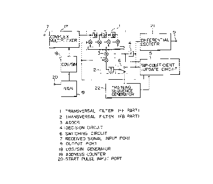
Referring to Fig. l, a complex multiplexes 17
performs an arithmetic operation for phase rotation of
an input signal that is input through an input port 7.
A COS/SIN generator 18 generates a phase of rotation which
is to be given to the complex multiplexes 17. An address
counter 19 determines data which is to be generated by the
COS/SIN generator 18. An input port 20 is used to input
a start pulse representative of the frame position of the
received signal. A differential decoder 21 differentially
decodes the output of the decision circuit 4. A training
sequence generator 22 outputs a known data sequence.
The operation of the adaptive equalizer shown in
Fig. 1 will be explained below.
First, a training sequence generating means in the
training sequence generator 22 of the adaptive equalizer
shown in Fig. 1 in a case where the received signal is a 1I/4
shifted QPSK modulation signal, will be explained with (1,
-l,l,-1,1,-l,-1,1,-1,-1,-1,1,1,1,-1,1,1,1,1,-1,-1,1,-1,
-1,1,-l, l,-1) taken as an example of a known transmission
data sequence bm.
(a) First, the known transmission data sequence bm is
serial-to-parallel converted, to obtain data sequences XK
and YK, and thereafter a data sequence CODE(K) is obtained
by encoding based on the code generation table shown in
Fig. 2.
Fig. 3 is a table showing the encoded data sequence
CODE(K).
(b) Next, assuming that CODE(1)=0, the encoded data
sequence CODE(K), shown in Fig. 3, is differentially
converted according to the following equation:
CODE(K)=MOD(CODE(K-1)+CODE(K),4)(K=2,15) (14a)
Fig. 4 is a table showing the encoded data sequence
CODE(K) which has been differentially converted according
to the above equation.
(c) Next, training data sequences COALR(K) and COBMR(K)
are generated from the data sequence CODE(K), shown in
Fig. 4, according to the conversion table shown in Fig. 5.
_23- z~~~~~~
Fig. 6 shows the result of the code generation, which
is the output data sequence of the training sequence
generator 22 of the adaptive equalizer shown in Fig 1.
The following is an explanation of elimination of
the 1I/4 phase rotation component in a case where the
received signal is a 1I/4 shifted QPSK modulation signal.
The address counter 19 is reset by the start pulse
representative of the frame position of the received signal,
and it outputs addresses to the COS/SIN generator 18
repeatedly in synchronism with the input timing of the
received signal such that if the received signal has been
subjected to symbol rate sampling, the address counter 19
outputs addresses (0,1,2,3,4,5,6,7), whereas, if the
received signal has been subjected to N samples/symbol it
outputs addresses (0,1,2,3,4,5,6,7...8N-1). The COS/SIN
generator 18 sends phases of rotation to the complex
multiplexes 17 according to the above addresses.
Fig. 7(a) is a table showing the relationship between
the addresses of the received signal that is input to the
adaptive equalizer and the phases of rotation generated by
the COS/SIN generator 18 in a case where the received signal
has been subjected to symbol rate sampling.
Fig. 7(b) is a table showing the relationship between
the addresses of the received signal that is input to the
adaptive equalizer and the phases of rotation generated by
the COS/SIN generator 18 in a case where the received signal
has been subjected to N-fold over sampling.
The complex multiplexes 17 performs an arithmetic
operation for phase-rotating the received signal.
Fig. 8 is a table showing a data sequence output
from the complex multiplexes 17 in a case where the received
signal that is input to the adaptive equalizer shown in
Fig. 1 has the data sequence shown in the table of Fig. 46
and the received signal has been subjected to symbol rate
sampling. The output data sequence of the complex
multiplexes 17 is the same as the data sequence obtained
by (5/4)1I phase-rotating each value in the output data
-24- ~~.~~ ~.
sequence of the training sequence generator 22 which is
shown in the table of Fig. 6.
The equalizer section that comprises the FF part 1,
the FB part 2, the adder 3, the decision circuit 4, the tap-
s coefficient-update circuit 5 and the switching circuit 6
is supplied with the result (X1K,XQK) of the arithmetic
operation executed in the complex multiplexer 17, and it
operates in the same way as the conventional adaptive
equalizer designed for QPSK modulation. That is, the
equalizer section effects equalization of the type in
which the input data is phase-rotated by -(5/4)11. The
output of the decision circuit 4 is sent to the differential
decoder 21.
Next, the operation of the differential decoder 21,
shown in Fig. 1, will be explained:
(a) First, a data sequence CODEF(K) is obtained from the
output data sequence of the decision circuit 4 according
to the code generation table that is shown in of Fig. 9.
Fig. 10 is a table showing the data sequence CODEF(K)
obtained when the output data sequence of the decision
circuit 4, shown in Fig. 1, is obtained from the output data
sequence (XIK,XQK) of the complex multiplexes 17, shown in
Fig. 8 by -(5/4)11 phase rotating in equalizer section.
(b) Next, the data sequence CODEF(K), which is shown in
Fig 10, is differentially decoded according to the
following equation:
CODEF(K)=~IOD(CODEF(K+1)-CODEF(K),4) (14b)
(c) Next, a decoded data sequence (XK',YK') is obtained
from the differentially decoded data sequence CODEF(K)
according to the decoded data sequence generation table
shown in Fig. 11.
Fig. 12 shows the decoded data sequence (XK',YK'),
which is obtained by converting the data sequence CODEF(X),
shown in Fig. 10, according to the decoded data sequence
generation table shown in Fig. 11. The decoded data
sequence (XK',YK') is parallel-to-serial converted to obtain
a data sequence shown below, which is coincident with the
known transmission data sequence bm:
-25-
(1,-1,1,-1,1,-1,-1,1,-1,-1,-1,1, , , , ,1,1,1,-1,-
1,1,-1,
-1,1,-1,1,-1)
Embodiment 2:
A second embodiment of the present invention will be
described below.
Fig. l3 is a block diagram showing Embodiment 2 of
the adaptive equalizer according to the present invention.
In the figure, the same elements as those in the prior art
are denoted by the same reference numerals, and description
thereof is omitted.
In Fig. 13, reference numeral 23 denotes a write
address counter, 24 a buffer memory for storing the received
signal, 25 a read address counter for reading data from the
memory 24, 26 a tap-coefficient-update circuit, and 27
an initialization circuit that initializes the tap-
coefficient-update circuit 26 and the tap-coefficients of
the FF and FB parts 1 and 2.
The operation of the adaptive equalizer shown in
Fig. l3 will be explained. Fig. 14 is a flowchart showing
the operation of the adaptive equalizer shown in Fig. 13.
First, the write address counter 23 is reset by the
start pulse representative of the frame position of the
received signal, and it generates and sends write addresses
to the memory 24 in synchronism with the input timing of
the received signal transmitted according to the burst
format shown in Fig. 43, which is input through the received
signal input port 7. .
The memory 24 stores the received signal in
accordance with the respective addresses.
The read address counter 25 causes the received
signal data corresponding to the UW 13, the random data a 14
and the CC 15 to be read out from the memory 24 and output
to the FF part 1, symbol by symbol.
The equalizer section that comprises the FF part 1,
the FB part 2, the adder 3, the decision circuit 4, the tap-
coefficient-update circuit 26 and the switching circuit 6
a
-26-
executes equalization of the UW 13, the random data a 14 and
the CC 15.
When the UW 13 is input (in the training mode), the
known training sequence UW 13; which is input through the
reference sequence input port 8, is input to the FB part 2
through the switching circuit 6, whereas, when the random
data a 14 and the CC 15 are input (in the tracking mode),
the output data sequence of the decision circuit 4 is input
to the FB part 2 through the switching circuit 6.
When the equalization of the CC 15 is completed, the
tap-coefficient-update circuit 26 sends a CC equalization
completion signal to the read address counter 25 and the
initialization circuit 27.
On receipt of the CC equalization completion signal,
the initialization circuit 27 initializes the tap-
coefficients of the FF and FB parts 1 and 2 and also
initializes the tap-coefficient-update circuit 26.
Here, the initialization of the tap-coefficients
corresponds to CM(0)=0 of Equation 12 in the prior art,
whereas the initialization of the tap-coefficient-update
circuit 26 is equivalent to executing P(0)=b lI of Equation
12.
In response to the CC equalization completion signal,
the read address counter 25 reads out the received signal
data corresponding to the CC 15 and the random data b 16
from the memory 24.
The equalizer section that comprises the FF part 1,
the FB part 2, the adder 3, the decision circuit 4, the tap-
coefficient-update circuit 26 and the switching circuit 6
executes retraining for the readout data by using the known
training sequence CC 15 and thereafter performs equalization
of the random data b 16.
When retraining is to be performed by using the known
training sequence CC 15, the data sequence input to the FB
Part 2 is changed by the switching circuit 6 to the known
training sequence CC 15 that is input through the reference
sequence input port 8, whereas, when the random data b 16
is to be equalized, the data sequence input to the FB part 2
-27-
is changed over to the output data sequence of the decision
circuit 4.
Embodiment 3:
A third embodiment of the present invention will be
described below.
Fig. 15 is a block diagram showing Embodiment 3 of
the adaptive~equalizer according to the present invention.
In the figure, the same elements as those in the prior art
are denoted by the same reference numerals, and description
thereof is omitted.
Referring to Fig. 15, a read address counter 28 reads
out data from the memory 24. Reference numeral 29 denotes
a tap-coefficient-update circuit, and 30 an equalized data
comparison circuit. An initialization circuit 31
initializes the tap-coefficient-update circuit 29 and
also initializes the tap-coefficients of the FF and FB
parts 1 and 2 on the basis of the result of comparison
made by the equalized data comparison circuit 30.
The operation of the adaptive equalizer shown in
Fig. 15 will be explained below. Fig. 16 is a flowchart
showing the operation of the adaptive equalizer shown in
Fig. 15.
The write address counter 23 is reset by the start
pulse representative of the frame position of the received
signal, and it generates and sends write addresses in
synchronism with the input timing of the received signal
that is transmitted according to the burst format shown
in Fig. 43.
In the memory 24, the received signal that is input
through the received signal input port 7 is stored in
accordance with the addresses generated. The read address
counter 28 causes the received signal data corresponding
to the UW 13, the random data a 14 and the CC 15 to be read
out from the memory 24 and output to the FF part 1, symbol
by symbol.
The equalizer section that comprises the FF part l,
the FB part 2, the adder 3, the decision circuit 4, the tap-
coefficient-update circuit 29 and the switching circuit 6
-28-
performs equalization of the UW 13, the random data a 14 and
the CC 15.
The tap-coefficient-update circuit 29 outputs the
result of the equalization of the received signal data
corresponding to the CC 15, that is, the result of the hard
decision made by the decision circuit 4, to the equalized
data comparison circuit 30, symbol by symbol.
The equalized data comparison circuit 30 makes
a comparison to decide whether or not the result of the
equalization of the received signal data corresponding to
the CC 15 is coincident with the known training.sequence
of the CC 15, and outputs the result of the comparison to
the initialization circuit 31 and the read address counter
28. When the comparison result reveals the equalized data
sequence is not coincident with the known training sequence,
the initialization circuit 31 acknowledges that the channel
estimation by the adaptive equalizer is not effectively
performed, and initializes the tap-coefficient-update
circuit 29 and the tap-coefficients of the FF and FB parts 1
and 2. When the equalized data sequence is coincident with
the known training sequence, initialization of the tap-
coefficient-update circuit 29 and the tap-coefficients is
not executed.
Here, the initialization of the tap-coefficients
corresponds to CM(0)=0 of Equation 12 in the prior art,
whereas the initialization of the tap-coefficient-update
circuit 29 is equivalent to executing P(0)=a lI of Equation
12.
When the comparison result reveals that the equalized
data sequence is not coincident with the known training
sequence, the read address counter 28 reads out the received
signal data corresponding to the CC 15 and the random data b
16 from the memory 24.
The equalizer section that comprises the FF part 1,
the FB part 2, the adder 3, the decision circuit 4, the tap-
coefficient-update circuit 29 and the switching circuit 6
executes retraining for the readout data by using the known
-29-
training sequence CC 15 and thereafter performs equalization
of the random data b 16.
When the equalized data sequence is coincident with
the known training sequence, the read address counter 28
reads out the received signal data corresponding to the
random data b 16 from the memory 24, and the equalizer
section that comprises the FF part 1, the FB part 2, the
adder 3, the decision circuit 4, the tap-coefficient-update
circuit 29 and the switching circuit 6 performs equalization
of the random data b 16 without retraining.
Embodiment 4:
A fourth embodiment of the present invention will be
described below.
Fig. 17 is a block diagram showing Embodiment 4 of
the adaptive equalizer according to the present invention.
In the figure, the same elements as those in the prior art
are denoted by the same reference numerals, and description
thereof is omitted.
Referring to Fig. 17, a memory 32 stores the receive d
signal, and a read address counter 33 reads out data from
the memory 32. Reference numeral 34 denotes a tap-
coefficient-update circuit, 35 a UW detector, and 36 a UW
detection output port.
The operation of the adaptive equalizer shown in
Fig. 17 will be explained below. Fig. 18 is a flowchart
showing the operation of the adaptive equalizer shown in
Fig. 17.
The write address counter 23 is reset by the start
pulse representative of the head of a burst, and thereafter
it generates addresses in synchronism with the input timing
of the received signal transmitted according to the burst
format shown in Fig. 43, which is input through the received
signal input port 7. The memory 32 stores the received
signal in accordance with the addresses generated. The
read address counter 33 causes the received signal data
corresponding to the UW 13 to be read out from the memory 32
and output to the FF part 1, symbol by symbol.
-30- ~~~
The equalizer section that comprises the FF part 1,
the FB part 2, the adder 3, the decision circuit 4, the tap-
coefficient-update circuit 34 and the switching circuit 6
executes an operation in the training mode (a) with respect
to the readout data, thereby updating the tap-coefficients.
After updating the tap-coefficients for the last UW
data in the received signal, the tap-coefficient-update
circuit 34 fixes the tap-coefficients of the FF and FB parts
1 and 2 to the last updated values and further sends
a training completion signal to the read address counter 33.
On receipt of the signal, the read address counter 33 causes
the received signal data corresponding to the UW 13 to be
read out from the memory 32 and output to the FF part 1
again, symbol by symbol. The data sequence input to the FB
part 2 at this time is the known training sequence UW 13,
which is input through the reference sequence input port 8.
The data input to the FF and FB parts 1 and 2 is
subjected to a product-sum operation together with the fixed
tap-coefficients, and the result of the operation undergoes
a hard decision in the decision circuit 4 and is then sent
to the UW detector 35.
The UW detector 35 makes a comparison between the
output data sequence of the decision circuit 4 and the known
training sequence UW 13 as a data sequence without decision
error. If these two data sequences are coincident with each
other, the UW detector 35 outputs a UW detection signal to
the UW detection output port 36, whereas, if the two data
sequences are not coincident with each other, the UW
detector 35 outputs a UW missed detection signal to the
output port 36.
After the completion of the UW detection, the UW
detector 35 sends a UW detection completion signal to the
read address counter 33. The read address counter 33 causes
the received signal data corresponding to the random data
a 14, the CC 15 and the random data b 16 to be read out from
the memory 32 and output to the FF part 1, symbol by symbol,
thereby effecting equalization sequentially.
-31-
Embodiment 5:
A fifth embodiment of the present invention will be
described below.
Fig. 19 is a block diagram showing Embodiment 5 of
the adaptive equalizer according to the present invention.
In the figure, the same elements as those in the prior art
are denoted by the same reference numerals, and description
thereof is omitted.
In Fig. 19, reference numeral 38 denotes a memory for
IO storing the received signal, 39 a complex multiplexer, and
40 a COS/SIN generator that gives the complex multiplexer 39
a COS/SIN value in accordance with the amount of phase
rotation to be made. An address counter 41 gives read
addresses to the memory 38 and also gives COS/SIN generation
data to the COS/SIN generator 40. A frequency offset
estimation circuit 42 estimates an offset frequency from
the result of the UW detection effected by the UW detector
35. A frequency offset compensation circuit 43 compensates
for the frequency offset of the received signal on the basis
of the result of the estimation made by the frequency offset
estimation circuit 42. Reference numeral 44 denotes
a complex multiplexer, 45 a COS/SIN generator that gives
phase rotation data to the complex multiplexer 44, and 46
an address counter that gives data for generating phase
rotation data to the COS/SIN generator 45.
The operation of the adaptive equalizer shown in
Fig. 19 will be explained below.
Fig. 21 is a flowchart showing the operation of
the adaptive equalizer shown in Fig. 19.
For the first burst of the signal received after
the beginning of communication, the frequency offset
compensation circuit 43 does not make compensation for
frequency offset, but outputs the received signal as it is.
The write address counter 23 is reset by the start pulse
representative of the head of the burst input through the
start pulse input port 20 and thereafter generates addresses
in synchronism with the input timing of the received signal
transmitted in the burst format shown in Fig. 43, which
A
-32- ~.~~.
is input through the received signal input port 7. The
memory 38 stores the received signal that is input through
the received signal input port 7 and passed through the
frequency offset compensation circuit 43 in accordance with
the addresses generated. The address counter 41 causes
the received signal data corresponding to the UW 13 to
be read out from the memory 38 and output to the complex
multiplexer 39, symbol by symbol. For this data, the
complex multiplexer 39 does not perform an arithmetic
operation for phase rotation by complex multiplication,
but outputs the data to the FF part 1 as it is.
For this input data, the equalizer section that
comprises the FF part 1, the FB part 2, the adder 3, the
decision circuit 4, the tap-coefficient-update circuit 34
and the switching circuit 6 updates the tap-coefficients
successively in the same way as in the operation of the
conventional adaptive equalizer in the training mode (a),
which has been set forth in the paragraph describing the
operation of the conventional adaptive equalizer designed
for QPSK modulation. After updating the tap-coefficients
for the last UW data in the received signal, the tap-
coefficient-update circuit 34 fixes the tap-coefficients
of the FF and FB parts 1 and 2 to the last updated values
and further sends a training completion signal to the
address counter 41. On receipt of the signal, the address
counter 41 causes the received signal data corresponding
to the UW 13 to be read out from the memory 38 and output
to the FF part 1, symbol by symbol, through the complex
multiplexer 39. The data sequence input to the FB part 2
at this time is the known training sequence UW 13, which
is input through the reference sequence input port 8.
The data that is input to the FF and FB parts 1 and 2 is
subjected to a product-sum operation together with the fixed
tap-coefficients, and the result of the operation undergoes
a hard decision in the decision circuit 4 and is sent to
the UW detector 35.
. -33-
The UW detector 35 makes a comparison between the
output data sequence of the decision circuit 4 and the known
training sequence UW 13 as a data sequence without decision
error. If these two data sequences are coincident with each
other, the UW detector 35 outputs a UW detection signal to
the frequency offset estimation circuit 42, whereas, if the
two data sequences are not coincident with each other, the
UW detector 35 outputs a UW missed detection signal to the
frequency offset estimation circuit 42. The frequency
offset estimation circuit 42 stores the result of the
comparison as a result of Of=0.
Upon completion of the UW detection for the data of
~f=0, the address counter 41 causes the memory 38 to output
received signal data corresponding to the UW 13 again and
also causes the COS/SIN generator 40 to generate fs(Hz)
phase rotation data.
The complex multiplexer 39 multiplies together
the received signal data corresponding to the UW 13 and
the phase rotation~data from the COS/SIN generator 40 to
give fs(Hz) phase rotation to the received signal data
corresponding to the UW 13. The data that has been fs(Hz)
phase-rotated is subjected to UW detection again by the
above-described method, and the result of the UW detection
is stored as a result of ~f=fs in the frequency offset
estimation circuit 42. Thereafter, UW detection is
similarly carried out on pieces of data which are obtained
by phase rotating the received signal data corresponding to
the UW 13 with ~f=0, ~fs, ~2fs, ~3fs, . . . . . . ,~Nfs,
respectively, and the results of the UW detection are
successively stored in the frequency offset estimation
circuit 42.
The frequency offset estimation circuit 42 finds
an average value of the frequencies with which UW has been
detected among Of=0, ~fs, ~2fs, ~3fs,......,~Nfs and estimates
the value that sign is inverted to be a frequency offset.
Fig. 20 is a table showing exemplarily the results
of U~'V detection for each phase rotation equivalent to ~f
-34-
In this example, UW is detected when Of=-fs, 0, +fs,
2fs and ifs, but no UW is detected on the other occasions;
therefore, the frequency offset of the received signal is
estimated to be -fs(Hz).
After the completion of the UW detection, the UW
detector 35 sends a UW detection completion signal to
the address counter 41. The address counter 41 causes
the received signal data corresponding to the random data
a 14, the CC 15 and the random data b 16 to be read out
from the memory 38 and output to the FF part 1 through the
complex multiplexes 39, symbol by symbol.
The equalizer section that comprises the FF part 1,
the FB part 2, the adder 3, the decision circuit 4, the tap-
coefficient-update circuit 34 and the switching circuit 6
performs equalization on the data corresponding to the
random data a 14, the CC 15 and the random data b 16
sequentially, as has been described in connection with
the prior art.
For the second burst and those following it, the
frequency offset estimated in the preceding burst is
compensated for in the frequency offset compensation circuit
43.
The operation of the frequency offset compensation
circuit 43 will be explained below.
After receiving the result of the estimation made
in the frequency offset estimation circuit 42, the address
counter 46 is reset by the start pulse representative of
the head of the burst input through the start pulse input
port 20, and thereafter it gives the COS/SIN generator 45
the address of the phase rotation data for making
compensation for the frequency offset which has been
estimated in the preceding burst.
The complex multiplexes 44 multiplies together the
received signal and the phase rotation data from the COS/SIN
generator 45 to give fs(Hz) phase rotation to the received
signal, thereby compensating for the frequency offset of the
received signal that is input to the adaptive equalizer.
-35-
It should be noted that frequency offset estimation
may also be made for each of the received signal data
following the first burst by the above-described method,
thereby compensating for each frequency offset estimated.
Embodiment 6:
A sixth embodiment of the present invention will be
described below.
Fig. 22 is a block diagram showing Embodiment 6 of
the adaptive equalizer according to the present invention.
In the figure, the same elements as those in the prior art
are denoted by the same reference numerals.
Referring to Fig. 22, a memory 47 stores the received
signal that is input to the adaptive equalizer. An address
counter 48 generates addresses for writing and reading data
to and from the memory 47. A frequency offset direction
estimation circuit 49 estimates a frequency offset direction
of the received signal. A frequency offset direction
detection circuit 50 detects a frequency offset direction
by averaging the results of estimation made by the frequency
offset direction estimation circuit 49. A frequency offset
compensation circuit 51 compensates for a frequency offset
of the received signal on the basis of the output of the
frequency offset direction detection circuit 50. Reference
numeral 52 denotes a complex multiplexes, 53 a COS/SIN
generator that generates phase rotation data for the complex
multiplexes 52, and 54 an address counter that gives the
COS/SIN generator 53 data for generating phase rotation
data.
The operation of the adaptive equalizer shown in
Fig. 22 will be explained below. Fig. 23 is a flowchart
showing the operation of the adaptive equalizer shown in
Fig. 22.
The frequency offset compensation circuit 51 does
not perform frequency offset compensation but outputs
the received signal as it is until a frequency offset
compensation signal is output from the frequency offset
direction detection circuit 50 with respect to the received
-36-
signal that is input through the received signal input
port 7.
The address counter 48 is reset by a start pulse
representative of the head of a burst input through the
start pulse input port 20, and thereafter it generates
write addresses in synchronism with the input timing of
the received signal that is input through the received
signal input port 7 and passed through the frequency-offset
compensation circuit 51.
The received signal that is output from the frequency
offset compensation circuit 51 is stored in the memory 47 in
accordance with the output of the address counter 48.
After an amount of input data which corresponds to
one symbol at the burst head has been stored in the memory
47, the address counter 48 generates read addresses.to cause
data to be read out from the memory 47 and input to the FF
part 1, symbol by symbol.
The interval of time at which data is read out from
the memory 47, symbol by symbol, is equal to or longer than
the interval at which the received signal is stored in the
memory 47, symbol by symbol.
For this input data, the equalizer section that
comprises the FF part 1, the FB part 2, the adder 3, the
decision circuit 4, the tap-coefficient-update circuit 34
and the switching circuit 6 updates the tap-coefficients
in the same way as in the operation of the conventional
adaptive equalizer in the training mode (a), which has
been set forth in the paragraph describing the operation
of the conventional adaptive equalizer designed for QPSK
modulation. After updating the tap-coefficients for the
last UW data in the received signal, the tap-coefficient-
update circuit 34 fixes the tap-coefficients of the FF
and FB parts 1 and 2 to the last updated values and further
sends a training completion signal to the address counter 48.
On receipt of the signal, the address counter 48
causes the received signal data corresponding to the UW 13
to be read out from the memory 38 and output to the FF part
1 again, symbol by symbol. The data sequence input to the
-37-
FB part 2 at this time is the known training sequence UW 13,
which is input through the reference sequence input port 8.
The data that is input to the FF and FB parts 1 and 2
is subjected to a product-sum operation together with the
fixed tap-coefficients, and the result of the operation is
sent to the frequency offset direction estimation circuit 49.
The frequency offset direction estimation circuit 49
finds a difference between the inner product obtained for
each symbol and the value of the UW 13, which is known, to
thereby calculate an error vector for each symbol, and sums
up the error vector values thus obtained.
If the received signal has a frequency offset, the
result of the product-sum operation is reflected on the
error vector; therefore, it is possible to estimate the
frequency offset direction (+ or -) of the received signal
from the sign of the result of the summation. The result
of the estimation is output to the frequency offset
compensation circuit 51.
After the completion of the frequency offset
direction estimation, the frequency offset direction
estimation circuit 49 sends a frequency offset direction
estimation completion signal to the address counter 48. On
receipt of the signal, the address counter 48 causes the
received signal data corresponding to the random data a 14,
the CC 15 and the random data b 16 to be read out from the
memory 24 and output to the FF part 1, symbol by symbol.
The equalizer section that comprises the FF part 1,
the FB part 2, the adder 3, the decision circuit 4, the tap-
coefficient-update circuit 34 and the switching circuit 6
Performs equalization on the above data sequentially.
The frequency offset direction detection circuit 50
stores the result of frequency offset direction estimation
for each burst, and after the estimation results for
a predetermined number of bursts have been stored, the
circuit 50 calculates the proportion of frequency offset
direction estimation results which show the same frequency
offset direction every predetermined number of bursts. If
the calculated proportion exceeds a predetermined level,
-38- 2~
the frequency offset direction detection circuit SO judges
that the frequency offset is present in this direction,
and outputs a frequency offset compensation signal and
the detected frequency offset direction to the frequency
offset compensation circuit 51.
The frequency offset compensation circuit 51 performs
frequency offset compensation with respect to the received
signal from the burst which is subsequent to the burst for
which the frequency offset.compensation signal is output
thereto.
The operation of the frequency offset compensation
circuit 51~wi11 be explained below.
After being reset by a start pulse representative of
the head of a burst input through the start pulse input port
20, the address counter 54 gives the COS/SIN generator 53
an address of phase rotation data that causes a predetermined
amount of change in the frequency in a direction in which
the frequency offset is compensated for, in accordance with
the input timing of the received signal input through the
received signal input port 7, from the burst subsequent to
the burst for which the frequency offset compensation signal
is sent to the circuit 51.
The complex multiplexer 52 multiplies together the
received signal and the phase rotation data output from the
COS/STN generator 53 to give ~f(Hz) phase rotation to the
received signal, thereby compensating for the frequency
offset of the received signal that is input to the adaptive
equalizer.
Embodiment 7:
A seventh embodiment of the present invention will be
described below.
Fig. 24 is a block diagram showing Embodiment 7 of
the receiver according to the present invention. In the
figure, the same elements as those in the prior art are
denoted by the same reference numerals, and detailed
description thereof is omitted.
M_. -39-
Referring to Fig. 24, a quasi-coherent detector 140
quasi-coherently detects a received IF signal. An input
port 141 is used to input a sample clock used when the
output of the quasi-coherent detector 140 is A/D converted.
A pair of A/D converters 142 and 143 convert quasi-
coherently detected Ich and Qch signals into digital
signals, respectively. A memory 144 stores data output
from the A/D converters 142 and 143. An address counter 145
operates on the clock supplied through the input port 141 to
send addresses to the memory 144. An incoherent correlator
146 determines correlation between the received data output
from the A/D converters 142 and 143 and the known
transmission data sequence UW 13 and outputs a correlation
value. A UW tentative detection circuit 147 detects
a tentative UW position from the output of the incoherent
correlator 146 and the output of the address counter 145
and outputs the tentative UW position thus detected. An
adaptive equalizer 148 recognizes the position of the UW 13
from the output of the UW tentative detection circuit 147,
equalizes data read out from the memory 144 and outputs
equalized Ich and Qch data, together with clock pulses. A
UW detector 103 is supplied with the output of the adaptive
equalizer 148 to effect final UW detection and outputs a U~V
detection signal. A frame synchronization control circuit
150 is supplied with the UW detection signal and the UW
tentative detection address to effect frame synchronization
control.
Fig. 25 is a block diagram showing the internal
arrangement of the incoherent correlator 146 shown in
Fig. 24.
In Fig. 25, reference numerals 160 and 161 denote
input ports for Ich data and Qch data, respectively. A
correlator No. 3 162 determines a correlation between the
data input through the input port 160 and Ich reference UW
data. A correlator No. 4 163 determines a correlation
between the data input through the input port 160 and Qch
reference UW data. A correlator No. 5 164 determines a
correlation between the data input through the input port
-40-
~m
161 and the Qch reference UW data. A correlator No. 6 165
determines a correlation between the data input through the
input port 161 and the Ich reference UW data. An adder 166
adds together the outputs of the correlators 162 and 164.
A subtracter 167 subtracts the output of the correlator 163
from the output of the correlator 165. A square-law circuit
168 squares the output of the adder 166. A square-law
circuit 169 squares the output of the subtracter 167. An
adder 170 adds together the outputs of the square-law
circuits 168 and 169. An output port 171 is used to deliver
the output of the adder 170 (i.e., a correlation value).
An input port 173 is used to input clock pulses for
activating the four correlators.
Fig. 26 is a block diagram showing the internal
arrangement of the UW tentative detection circuit 147.
Referring to Fig. 26, an input port 180 is used
to input the output value of the address counter 145. An
input port 181 is used to input the output of the incoherent
correlator 146. A comparator 182 makes a comparison between
the output value (correlation value) of the incoherent
correlator 146 and a predetermined threshold B, and if
the correlation value Z B, the comparator 182 outputs
a tentative UW detection signal. A flip-flop 183 latches
the output value of the address counter 145 on the basis
of the output of the comparator 182. An output port 184 is
used to deliver the output value (tentative UW position) of
the flip-flop 183 to the outside.
Fig. 27 is a block diagram showing exemplarily the
internal arrangement of the adaptive equalizer 148. In the
figure, the same elements as those in Fig. 17, which shows
Embodiment 4, are denoted by the same reference numerals,
and detailed description thereof is omitted.
Referring to Fig. 27, a U~i' address input port 55 is
used to input an address in the memory 144 where the head
of UW data has been written. A read address counter 56
designates a read address in the memory 144. Reference
numeral 57 denotes an output port for outputting equalized
UW data, and 62 an address output port.
-41- ~3
The operation of the receiver shown in Fig. 24 will
be explained below.
The received IF signal is converted into two
orthogonal quasi-coherent signals in the quasi-coherent
detector 140. The quasi-coherent signals are assumed to
be expressed by complex representation as follows:
V(t)=K~exp(j(~wt+8(t)+D9)))
=K~{a(t)+jb(t)}~exp(J(owt+o8) (15)
where K is the amplitude; ~w is the difference
between the center frequency of the received signal and
the frequency oscillated by a local oscillator for quasi-
coherent detection; D8 is the initial phase difference
between the received signal and the local oscillator output;
8(t) is the modulation component; and a(t) and b(t) are Ich
and Qch baseband signals, respectively.
Assuming, for simplification, that Ow=0 and that the
A/D converters are adapted for symbol interval sampling at
Nyquist point, the A/D converter output is represented by
V(nT)=K'{a(nT)+jb(nT)}~exp(j~8) (16)
In the above equation, V(nT) is a sampled data which
is stored in the memory 144 and also input to the incoherent
correlator 146. Further, the sample clock is input to the_
address counter 145 to designate an address in the memory
144.
The real part (Ich component) of V(nT) that is input
to the incoherent correlator 146 is input to the correlators
162 and 163 through the input port 160, while the imaginary
part (Qch component) is input to the correlators 164 and
165. Each correlator operates on the basis of the sample
clock supplied through the input port 173.
A reference UW pattern comprising a known training
sequence inside the incoherent correlator 146 is represented
by
UW(i)=R(i)-jIm(i) (17)
where i=1 to N; N: UW length (symbol)
In the above equation, R(i) is the Ich UW reference
pattern, and Im(i) the Qch UW reference pattern.
. _ ~-_,~
-42-
Data that is stored in the i-th shift registers
in the correlators 162, 163, 164 and 165 at time nT is
represented by
Vnt(i)=K'{anT(i)+jbnT(i)}~exp(j~8) (18)
The incoherent correlator 146 sums up the complex
products of the respective parts of Equations 17 and 18 as
follows
N
C(nT)= ~ VnT(iO UW(i)
i=1
N
K~{anT(i)+jbnT(1)}~exp(JO8)
i=1
{R(i)-jIm(i)}
=K~exP(J~8)~{X(nT)+jY(nT)} (19)
Here, X(nT) and Y(nT) are represented by
N
X(nT)= ~ {anT(i)R(i)+bnT(i)Im(i)}
i=1
N
Y(nT)= ~ {R(i)bnT(i)-Im(i)anT(i)}
i=1
Assuming that the UW 13 is input to the incoherent
correlator 146 without noise,
anT(i)=R(i)~ bnT(i)=Im(i)
Assuming that R(i)=~1 and Im(i)=~1, for example,
C(nT) is represented by
CUW(nT)=K~exp(j06)
N
y{R(i)2-Im(i)2+j(R(i)Im(i)-Im(i)R(i))}
1=1
=K-exp(j~8){2N+JO} (20)~
When no UW 13 is input, the probability that
anT(i)=R(i) and bnT(i)=Im(i) will be valid is 1/2 each, and
C(nT) that satisfies the condition of ~CUW(nT)~ ~ ~C(nT)~ is
output.
-43-
Incidentally, the real and imaginary parts of C(nT)
correspond to the respective outputs of the adder 166 and
the subtracter 167. The real and imaginary parts of C(nT)
are squared in the square-law circuits 168 and 169,
respectively, and then added together in the adder 170 as
follows:
Z(nt)=[real{C(nT)}]2+[imag{C(nT))}]2 (21)
=[K{X(nT)cos(o8)-Y(nT)sin(~8)}]2
+[K{X(nT)sin(~8)+Y(nT)cos(~6)}]2 (22)
If C(nT)=CUW(nT), then
ZUW(nT)
={K~X(nT)cos(~9)}2+{K~X(nT)sin(~8)}2
=4K2N2 (23)
Therefore, the adder 170 outputs 4K2N2 when
C(nT)=CUW(nT), and it outputs a relatively small value on
other occasions. The correlation value thus calculated is
output from the incoherent correlator 146 through the output
port 171 so as to be input to the UW tentative detection
circuit 147.
Although it is assumed that R(i)=tl and Im(i)=il in
the foregoing for simplification, it should be noted that
R(i) and Im(i) do not necessarily need to be binaries and
that these may be analog values.
The operation of the UW tentative detection circuit
147 will be explained below.
In the UW tentative detection circuit 147, the
correlation value output from the incoherent correlator 146
is compared with a predetermined threshold B.
Here, a value for the threshold B with which the UW
13 is tentatively detected on condition that the correlation
value ? the threshold B is set in advance. Assuming that
the correlation value >_ the threshold B, the comparator 182
outputs a tentative UW detection signal, so that the flip-
flop 183, which is triggered by the tentative UW detection
signal, latches the address in the memory 144 where the UW
data has been written and outputs it through the port 184.
'44- ~ ,~ ~i
The adaptive equalizer 148 will next be explained
with reference to Fig. 27.
The adaptive equalizer 148 recognizes the address in
the memory 144 where the received signal data corresponding
to the UW 13 has been written from address information
output from the UW tentative detection circuit 147, which
is input thereto through the UW address input port 55, and
causes the read address counter 56 to fetch the received
signal data corresponding to the UW 13 from the memory 144.
The equalizer section that comprises the FF part l,
the FB part 2, the adder 3, the decision circuit 4, the tap-
coefficient-update circuit 34 and the switching circuit 6
subjects the readout data to an operation carried out in
the training mode (a), as has been set forth in the
Paragraph describing the operation of the conventional
adaptive equalizer designed for QPSK modulation, thereby
updating the tap-coefficients successively.
After updating the tap-coefficients for the last
data in the received signal corresponding to the known
transmission data sequence UW 13, the tap-coefficient-update
circuit 34 fixes the tap-coefficients of the FF and FB
parts 1 and 2 to the last updated values and further sends
a training completion signal to the read address counter 56.
On receipt of the signal, the read address counter 56
causes the received signal data corresponding to the UW 13
to be read out from the memory 144 and output to the FF part
1, symbol by symbol. The data sequence input to the FB part
2 at this time is the known training sequence UW 13, which
is input through the reference sequence input port 8.
The data that is input to the FF and FB parts 1 and 2
is subjected to a product-sum operation together with the
fixed tap-coefficients, and the result of the operation
undergoes a hard decision in the decision circuit 4 and is
sent to the UW detector 103 through the UW data output port
57.
The UW detector 103 receives the coherently detected
UW data, which has been equalized in the adaptive equalizer
148, determines a correlation between the UW data and the
_45-
reference UW pattern by a method similar to that in the
prior art shown in Fig. 49, and outputs either a UW
detection signal or a UW missed detection signal.
Then, the respective outputs of the UW detector 103
and the UW tentative detection circuit 147 are input to
the frame synchronization control circuit 150.
When it receives a UW detection signal, the frame
synchronization control circuit 150 recognizes the position
of the UW from the output of the UW tentative detection
circuit 147 and starts frame synchronization control such
as aperture control.
On the other hand, when it receives a UW missed
detection signal, the frame synchronization control circuit
150 ignores the output value of the UW tentative detection
circuit 147 and reexecutes the acquisition operation.
Although in the foregoing description the sample
clock for A/D conversion is arranged to effect symbol
interval sampling at Nyquist point, it should be noted that
the same advantageous effects can also be obtained by
carrying out oversampling wherein sampling is executed 2
or more times per symbol.
Embodiment 8:
An eighth embodiment of the present invention will be
described below.
In the foregoing Embodiment 7, a tentative UW
position is determined by making a comparison between
a correlation value and a predetermined threshold inside
the UW tentative detection circuit 147. However, it is
also possible to obtain the same advantageous effects by
detecting the maximum value in the output of the incoherent
correlator 146 within an aperture (within one frame in
a case where there is no aperture) and defining the address
of the maximum value as a tentative UW position.
Fig. 28 is a block diagram showing Embodiment 8 of
the receiver according to the present invention. In the
figure, the same elements as those in Fig. 24, which shows
Embodiment 7, are denoted by the same reference numerals,
and description thereof is omitted.
-46-
Referring to Fig. 28, an input port 190 is used to
input a gate signal for aperture gate, frame gate or the
like. A UW tentative detection circuit 191 is supplied
with the output of the address counter 145, the output of
the incoherent correlator 146 and the gate signal to detect
a tentative UW position.
Fig. 29 is a block diagram showing the internal
arrangement of the UW tentative detection circuit 191.
In Fig. 29, reference numeral 192 denotes an input
Port for the output value of the address counter 145, 193
an input port for the output value of the incoherent
correlator 146, and 194 an input port for the gate signal.
A gate circuit 195 enables or disables the comparator output
pulse in response to the gate signal. A flip-flop 196
latches the output value of the incoherent correlator 146
in response to the output pulse of the gate circuit 195.
A comparator 197 makes a comparison between the output value
of the incoherent correlator 146 and the output value of
the flip-flop 196 and outputs a pulse when the output value
of the incoherent correlator 146 z the output value of the
flip-flop 197. A flip-flop 198 latches the output value of
the address counter 145 in response to the output pulse of
the gate circuit 195. An output port 199 is used to deliver
the output of the flip-flop 198 to the outside.
In Fig. 28, the incoherent correlator 146 outputs
a correlation value at every sample timing, and the
correlation value is input to the comparator 197 through
the input port 193.
When the input correlation value is smaller than
the output value of the flip-flop 196, the comparator 197
outputs nothing, whereas, when the correlation value is
larger than the output value of the flip-flop 196, the
comparator 197 outputs a pulse. At this time, if the gate
signal supplied through the input port 194 is ON, the pulse
output from the comparator 197 passes through the gate
circuit 195 to latch the correlation value in the flip-flop
196. Thus, the maximum correlation value in the gate range
is latched in the flip-flop 196. At the same time, the
-47-
pulse output from the gate 195 is input to the flip-flop
198, so that the flip-flop 198 stores a memory address where
the maximum correlation value is stored.
The adaptive equalizer 148 recognizes a tentative
UW position from the maximum correlation value through the
output port 199 and then starts training.
Embodiment 9:
A ninth embodiment of the present invention will be
described below.
Fig. 30 is a block diagram showing Embodiment 9 of
the receiver according to the present invention. In the
figure, the same elements as those in Figs. 1 and 28, which
show Embodiments 1 and 7, respectively, are denoted by the
same reference numerals, and description thereof is omitted.
In the foregoing Embodiment 7, the outputs of the A/D
converters 142 and 143 are input directly to the incoherent
correlator 146 and the memory 144. However, in a case where
the received signal is a Tt/4 shifted QPSK modulation signal,
a 1I/4 phase rotation component elimination circuit may be
added at the back of the A/D converters 142 and 143. With
this alternative arrangement also, the same advantageous
effects are obtained.
Embodiment 10:
A tenth embodiment of the present invention will be
described below.
Fig. 31 is a block diagram showing Embodiment 10 of
the receiver according to the present invention. In the
figure, the same elements as those in Fig. 24,.which~shows
Embodiment 7, are denoted by the same reference numerals,
and description thereof is omitted.
Referring to Fig. 31, hard-decision circuits 200 and
201 make a hard decision on the output values of the A/D
converters 142 and 143, respectively. A selector 202
selects either the outputs of the A/D converters 142 and 143
or the outputs of the hard-decision circuits 200 and 201.
An input port 203 is used to input a select signal for the
selector 202.
-48-
The operation of the receiver shown in Fig. 31 will
be explained below.
In a case where the variance of input signal level
due to fading cannot be ignored in the time range for
searching when the receiver effects UW detection (e. g.,
in a case where there is no aperture and UW is detected
in a long period of time, i.e., at the time of hand off
or initial acquisition), the complex representation of the
outputs of the A/D converters 142 and 143 is as follows:
Vr(nT)=K(nT)~{a(nT)+jb(nT)}~exp(j~8) (24)
where K(nT) is the amplitude, a(nT) the Ich baseband
signal, b(nT) the Qch baseband signal, and D8 the initial
phase difference between the input signal and the local
oscillator output for quasi-coherent detection.
Therefore, assuming that the input level is constant
within the time equivalent to the UW length, the output
value of the incoherent correlator 146 is represented by
Zr(nT)=4K2(nT)N2 (25)
As will be understood from the above equation,
since the amplitude term is time-varying, the output of the
incoherent correlator 146 cannot be determined by the data
pattern alone. Thus, UW detection is difficult to effect.
Therefore, at the time of hand off, for example,
the outputs of the hard-decision circuits 200 and 201 are
selected as input signals to the incoherent correlator 146
by using a select signal input through the port 203.
The complex representation of the outputs of the
hard-decision circuits 200 and 201 is as follows:
VH(nT)={aH(nT)+jbH(nT)}~exp(j8m) (26)
where 8m=0 , tlI/2 , Tf
In the above equation, aH(nT) and bH(nT) correspond
to a(nT) and b(nT), respectively, in Equation 16, and the
hard-decision value 8m represents the ambiguity of the
Phase.
The output value of the incoherent correlator 146
at this time is represented by
ZH(nT)=[{X(nT)cos(6m)-Y(nT)sin(8m)}]2
+[{X(nT)sin(6m)+Y(nT)cos(8m)}]2 (27)
-4g-
The output obtained when the UW pattern is input is
represented by the following equation; it is independent of
the amplitude of the input signal:
Z~H(nT)=4N2 (28)
The UW tentative detection circuit 191 receives the
output of the incoherent correlator 146 which has got rid of
the variance of input signal level and detects a tentative
UW position by the threshold method or the maximum value
detecting method.
The adaptive equalizer 148 recognizes the address in
the memory 144 where the received signal data corresponding
to the UW 13 has been written from the output of the UW
tentative detection circuit 191, and fetches the data
corresponding to the UW 13 from the memory 144.
The adaptive equalizer 148 equalizes the received
signal data corresponding to the UW 13 and outputs the
equalized data to the UW detector 103, as described in
Embodiment 7.
The UW detector 103 receives the UW data which has
been subjected to the coherent detection and equalized by
the adaptive equalizer 148, determines a correlation between
the equalized UW data and the reference UW pattern by the
same method as in the prior art, and outputs either a UW
detection signal or a UW missed detection signal.
Then, the output of the UW detector 103 and the
output of the UW tentative detection circuit 191 are input
to the frame synchronization control circuit 150.
When it receives a UW detection signal, the frame
synchronization control circuit 150 recognizes the UW
position from the output of the UW tentative detection
circuit 191 and starts frame synchronization control such
as aperture control.
On the other hand, when it receives a UW missed
detection signal, the frame synchronization control circuit
150 ignores the output value from the UW tentative detection
circuit 191 and reexecutes the acquisition operation.
-50-
In a stationary state, normally, the input signal
level does not change substantially as far as the output
of the incoherent correlator 146 is seen through the
aperture. Therefore, the selector 202 is changed over by
using a select signal supplied through the input port 203
so that the signals input to the incoherent correlator 146
are changed over to the soft-decision values, thereby
enabling the system to operate normally even in the presence
of frequency selective fading.
Fig. 32 shows an example of the select signal used
to change over the selector 202.
The select signal is arranged such that during the
initial acquisition, the hard-decision values are selected
as those input to the incoherent correlator 146, whereas,
during the stationary state, the soft-decision values are
selected.
Embodiment 11:
An eleventh embodiment of the present invention will
be described below.
Fig. 33 is a block diagram showing Embodiment 11 of
the receiver according to the present invention. In the
figure, the same elements as those in Fig. 31, which shows
Embodiment 10, are denoted by the same reference numerals,
and description thereof is omitted.
In the foregoing Embodiment 10, at the time of
initial acquisition the signals input to the incoherent
correlator 146 are changed over to the hard-decision_signals
to thereby eliminate the influence of the variance of input
signal level due to fading. However, an automatic gain
control (hereinafter referred to as "AGC") may be provided
in the IF part (or the RF part) or the input part of the
incoherent correlator 146 to effect changeover control
such that the response speed (time constant) of the AGC
during the initial acquisition varies from that during
the stationary state. With this arrangement also, the
same advantages are obtained.
-51-
In Fig. 33, reference numeral 210 denotes an AGC
amplifier. An AGC detector 211 detects the output level of
the AGC amplifier 210. A loop filter (LFa) 212 averages the
output values of the AGC detector 211. A loop filter (LFb)
213 also averages the output values of the AGC detector 211.
A selector 114 selects the output of the LFa 212 or the
output of the LFb 213. The output of the selector 114 is
connected to a control terminal of the AGC amplifier 210.
The operation will next be explained. Referring to
Fig. 33, the received signal is input to the AGC amplifier
210 through the input port 101. The output of the AGC
amplifier 210 is branched into two. One of them is input to
the quasi-coherent detector 140, while the other is input to
the AGC detector 211.
The AGC detector 211 outputs a voltage value in
accordance with the input electric power, and the output
voltage value is input to both the LFa 212 and the LFb 213.
It is assumed that the time constant of the LFa 212 is
substantially equal. to the UW length and that the time
constant of the LFb 213 is sufficiently larger than that
of the LFa 212.
At the time of initial acquisition, the selector 214
selects the output of the LFa 212 in response to the select
signal supplied through the input port 203. Since the time
constant of the LFa 212 is substantially equal to the UW
length, as has been stated above, if the input signal level
becomes constant within the time equivalent to the UW
length, the output level of the AGC amplifier 210 becomes
substantially constant. Accordingly, the variance of input
signal level due to fading has already been substantially
eliminated from the received signal when input to the quasi-
coherent detector 140, so that it is possible to effect UW
tentative detection of high accuracy.
During the stationary state, the influence of the
variance of input signal level is eliminated by the aperture
effect; therefore, a larger time constant of the AGC is
preferable with a view to reducing the effect of noise.
-52_ ~ ~ ~ a.
Accordingly, during the stationary state, the
selector 214 selects the output of the LFb 213 in response
to the select signal supplied through the input port 203.
Embodiment 12:
A twelfth embodiment of the present invention will be
described below.
Fig. 34 is a block diagram showing Embodiment 12 of
the receiver according to the present invention. In the
figure, the same elements as those in Fig. 31, which shows
Embodiment 10, are denoted by the same reference numerals,
and description thereof is omitted.
Referring to Fig. 34, a memory 220 stores the outputs
of the A/D converters 142 and 143. A complex multiplexer
221 phase-rotates the output value of the memory 220. A
COS/SIN generator 222 gives the complex multiplexes 221
a COS/SIN value in accordance with the amount of phase
rotation to be made. A frequency sweeper 223 gives phase
rotation data to the COS/SIN generator 222 by sweep
frequency and stores a frequency with which the incoherent
correlator 146 outputs the maximum value. A peak detection
circuit 224 outputs a maximum value detection pulse to
the frequency sweeper 223 when the incoherent correlator 146
outputs the maximum value and also outputs a timing at
which the output of the incoherent correlator 146 reaches
a maximum. A memory 225 stores UW data phase-rotated with
several different frequencies by the complex multiplexes
221. An adaptive equalizer 226 equalizes the output of the
memory 225. A controller 227 is supplied with the. address
of the maximum value of the output from the peak detection
circuit 224, and it designates a read address in the memory
220 and also a write address in the memory 225 and further
sends a control signal to the frequency sweeper 223, a reset
signal and aperture gate to the peak detection circuit 224,
a select signal to the selector 202 and a start pulse to
the adaptive equalizer 226. A frame synchronization control
circuit 228 is supplied with the output of the UW detector
103 and the output of the peak detection circuit 224 and
delivers a control signal to the controller 227.
A
_... -5 3-
Fig. 35 is a block diagram showing exemplarily the
arrangement of the adaptive equalizer 226, which is the same
as Fig. 27 that shows the adaptive equalizer 148 illustrated
in Embodiment 7; therefore, description thereof is omitted.
The operation of the receiver shown in Fig. 34 will
be explained below.
Fig. 36 is a flowchart showing the operation of the
receiver shown in Fig. 34.
It is assumed that the memory 220 is stored with data
consisting of 1 burst + a length (or 1 frame + a length) so
that UW data is contained therein without fail.
The data stored in the memory 220 is read out in
accordance with the read address output from the controller
227 and phase-rotated with a frequency designated in the
frequency sweeper 223. The output of the complex
multiplexer 221 is input to the incoherent correlator 146.
At this time, hard decision is selected for the selector 202
by the controller 227.
The output of the incoherent correlator 146 is input
to the peak detection circuit 224, together with the read
address in the memory 220. When the output value of the
incoherent correlator 146 is the largest of the values
input to the peak detection circuit 224, the peak detection
circuit 224 stores the timing at which the maximum value is
input thereto and further sends a maximum value detection
pulse to the frequency sweeper 223.
On receipt of the maximum value detection pulse, the
frequency sweeper 223 stores the frequency with which the
maximum value is output. The above operation is executed
in the frequency range to be considered by using the first
frequency step (aF).
As a result of the above operation executed for
several different frequencies, the peak detection circuit
224 is stored with the timing Imax (that is, the address
written in the memory 220) at which the maximum value is
output from the incoherent correlator 146, while the
frequency sweeper 223 is stored with the frequency Fmax. At
this time, the controller 227 is supplied with the maximum
-54-
value output timing, which is decided to be a tentative UW
position of the burst (or frame) concerned.
Next, the controller 227 extracts only the UW data
from the memory 220 by using the tentative UW position Imax,
and phase-rotates the UW data around the frequency Fmax by
using the second frequency step (of).
The phase-rotated UW data is input to the incoherent
correlator 146, At this time, the selector 202 selects
soft-decision outputs in order to eliminate the influence
of the initial phase.
Then, the output of the incoherent correlator 146 is
input to the peak detection circuit 224. At this time, the
timing for maximum value detection is limited to Imax only
by the aperture sent from the controller 227; therefore, the
Peak detection circuit 224 executes only frequency search.
When the maximum correlation value based on the soft-
decision UW data is input thereto, the peak detection
circuit 224 sends a maximum value detection pulse to the
frequency sweeper 223. In response to the maximum value
detection pulse, the frequency sweeper 223 stores the
frequency at which the maximum value has been output.
It should be noted that the maximum correlation value
that is stored in the peak detection circuit 224 is reset
by a reset signal from the controller 227 before the hard
decision shifts to the soft decision.
This operation is executed in the second frequency
range to be considered. After the completion of the
frequency sweep, the frequency sweeper 223 is stored with
the frequency (fmax) with which the maximum soft-decision
correlation value is output at Imax.
The foregoing processes are the tentative UW position
detection and the coarse frequency offset detection.
Next, the controller 227 extracts only the LTW data by
using Imax, phase-rotates the UW data around the frequency
fmax by using the third frequency step (~df) and writes the
data in the memory 225.
It should be noted that the write address in the
memory 225 is given by the controller 227.
_55_
In addition, the frequency step (~df) is set so that
any one of the frequencies swept falls into the range in
which the adaptive equalizer 226 is operatable.
This operation is executed in the third frequency
range to be considered, and as a result, the memory 225 is
stored with the UW pattern phase-rotated with several
different frequencies.
The adaptive equalizer 226 activates the read address
counter 59 in response to a start pulse supplied from
the controller 227 to fetch the received signal data
corresponding to the UW 13, which has been phase-rotated
with a certain frequency, from the memory 225.
The equalizer 226 that comprises the FF part 1, the
FB part 2, the adder 3, the decision circuit 4, the tap-
coefficient-update circuit 34 and the switching circuit 6
performs equalization on the data fetched from the memory
225.
After updating the tap-coefficients for the Last UW
data in the received signal, the tap-coefficient-update
circuit 34 fixes the tap-coefficients of the FF and FB parts
1 and 2 to the last updated values, and sends a training
completion signal to the read address counter 59.
On receipt of the signal, the read address counter 59
causes the received signal data corresponding to the UW 13
to be read out from the memory 144 and output to the FF part
1 again, symbol by symbol.
The data sequence that is input to the FB part 2 at
this time is the known training sequence UW 13, which is
input through the reference sequence input port 8.
The data that is input to the FF and FB parts 1 and 2
are subjected to a product-sum operation together with the
fixed tap-coefficients. The result of the operation
undergoes a hard decision in the decision circuit 4 and
then output to the UW data output port 57.
The UW detector 103 receives the UW data which has
already been subjected to coherent detection and equalized
in the adaptive equalizer 226, determines a correlation
between the UW data and the reference UW pattern by the same
_56_
method as in the prior art, and outputs either a UW
detection signal or a UW missed detection signal.
Then, the output of the UW detector 103 and the
output of the peak detection circuit 224 are input to the
frame synchronization control circuit 228. When a UW
detection signal is input thereto, the frame synchronization
control circuit 228 recognizes the UW position from the
output of the peak detection circuit 224 and then starts
frame synchronization control such as aperture control.
At the same time, the frame synchronization control
circuit 228 sends a control signal to the controller 227 to
cancel the initial acquisition mode. When a UW missed
detection signal is output from the UW detector 103, the
adaptive equalizer 226 reads out UW data phase-rotated with
a different frequency from the memory 225 and repeats the
above-described operation.
If no UW detection signal is detected even when the
above-described operation is executed for all the UW data
stored in the memory 225, UW false detection is declared for
the burst (or frame) concerned, and the initial acquisition
operation is then executed for the subsequent burst (or
frame) from the hard-decision correlation determination.
Embodiment 13:
A thirteenth embodiment of the present invention will
be described below.
Fig. 37 is a block diagram showing Embodiment 13 of
the receiver according to the present invention. In the
figure, the same elements as those in Fig. 34, which shows
Embodiment 12, are denoted by the same reference numerals,
and detailed description thereof is omitted.
In Fig. 37, reference numeral 230 denotes an input
port for a received IF (or RF) signal, and 231 a mixer for
frequency conversion of the received signal. A VCO 232
outputs a local oscillation signal which is input to the
mixer 231. A band pass filter (hereinafter referred to as
"BPF") 233 eliminates an unnecessary frequency component
from the output of the mixer 231. A frequency sweeper 234
gives phase rotation data to the COS/SIN generator 222 and
a
-57-
stores and outputs a frequency with which the incoherent
correlator 146 outputs the maximum value.
A frame synchronization control circuit 235 is
supplied with the respective outputs of the UW detector 103,
the peak detection circuit 224 and the frequency sweeper
234, and it sends a control signal to the controller 227 and
effects frame synchronization control and local control. A
D/A converter 236 D/A converts a signal that is output from
the frame synchronization control circuit 235 to control the
V~0 232.
The operation of the receiver shown in Fig. 37 will
be explained below.
It is assumed that the coarse frequency offset
detection and the tentative UW position detection have
already been completed in the initial acquisition operation
and that pieces of UW data phase-rotated with several
frequencies have already been written in the memory 225.
First, the coarse frequency offset information (fmax)
stored in the frequency sweeper 234 and the output (Imax) of
the peak detection circuit 224 are input to the frame
synchronization control circuit 235. Then, the controller
227 gives a start pulse to the adaptive equalizer 226.
The adaptive equalizer 226 fetches the phase-rotated
UW data from the memory 225. The adaptive equalizer 226
equalizes the fetched data and outputs the equalized data to
the UW detector 103, as has been described in Embodiment 12.
The UW detector 103 receives the UW data which has
been subjected to the coherent detection and equalized in
the adaptive equalizer 226, determines a correlation between
the equalized UW data and the reference UW pattern by the
same method as in the prior art, and outputs either a UW
detection signal or a UW missed detection signal.
The above-described processing is executed for all
the UW data stored in the memory 225. If the third start
frequency, the third frequency step (~df) and the number
of times of sweep are known in advance (these conditions
can be made known by previously giving rotating frequency
information used in the frequency sweeper 234 to the
_5g_
frame synchronization control circuit 235), the frame
synchronization control circuit 235 can find the frequency
offset of each UW data processed by the adaptive equalizer
226 on the basis of the sequence in which UW data are
written in the memory 225 and the coarse frequency offset
information (fmax).
In this way, UW detection or UW missed detection is
decided for each frequency offset, and a table such as that
shown in Fig. 38 is generated in the frame synchronization
control circuit 235.
Then, the frame synchronization control circuit 235
averages the frequencies with which UW has been detected,
and decides the average frequency offset dFave to be the
frequency offset of the burst (or frame) concerned. The
frame synchronization control circuit 235 then sends
a signal equivalent to that frequency to the D/A converter
236.
The D/A converter 236 converts the frequency signal
into an analog voltage, thereby controlling the frequency
oscillated by the VCO 232, and thus making constant the
frequency of the subsequent signal input to the quasi-
coherent detector 140.
If no UW is detected from all the UW data stored in
the memory 225 (i.e., if UW missed detection is decided for
all the UW data), UW false detection is declared for the
burst (or frame) concerned, and the initial acquisition
operation is then executed for the subsequent burst (or
frame).
Embodiment 14:
. A fourteenth embodiment of the present invention will
be described below.
In a case where the VCO 232 is controlled as in
Embodiment 13, no satisfactory accuracy can be obtained by
a single control operation when the receiver shifts from
the initial acquisition mode to the static mode due to the
following control error factors:
(a) Error due to variations in the accuracy of the V/F
characteristics of the VCO 232.
A
(b) Error due to the accuracy of the Odf step.
(c) Error due to Doppler effect in the fading channel or
random FM.
(d) Measuring error due to Gaussian noise.
Accordingly, it is necessary to improve the accuracy
by effecting the control a plurality of times.
In general, when a receiver effects frame
synchronization control, the initial acquisition mode does
not shift directly to the static mode, but a back protection
mode is interposed between these two modes.
Fig. 39 is a state transition graph, which is shown
in the above-mentioned literature, i.e., Yamamoto and Kato,
"TDMA Communications", the Institute of Electronics,
Information and Communication Engineers (1989), pp.2l.
The following is a description of the way in which
the accuracy of frequency control is improved before the
receiver shifts to the static mode by making use of the back
protection mode used in the frame synchronization control.
The frame synchronization control and frequency
control in Embodiment 13 correspond to the initial
acquisition mode shown in Fig. 39. Accordingly, the
receiver shifts to the back protection mode and then
executes similar processing with respect to the data stored
in the memory 220.
However, since the UW position is known at this time,
it is possible to apply an aperture, and soft-decision data
is employed as data input to the incoherent correlator 146.
Then, the peak detection circuit 224 obtains timing
at which the incoherent correlator 146 outputs the maximum
value within the aperture with respect to UW neighboring
data phase-rotated with several different frequencies,
thereby detecting a tentative UW position (Imax2) for the
second burst (or frame). At the same time, coarse frequency
offset information (fmax2) is obtained from the frequency
with which the maximum value is output.
Next, UW data that is obtafined from the tentative UW
position (Imax2) is phase-rotated with several different
frequencies around the coarse frequency offset information
-60-
(fmax2), and the phase-rotated UW data is then sent to the
memory 225, in the same way as in Embodiment'13.
It should be noted that the search range and
frequency step used in this back protection mode are finer
than those used in the initial acquisition mode. The
adaptive equalizer 226 equalizes the UW data read out from
the memory 225, effects UW detection by using the equalized
data, and prepares a table such as that shown in Fig. 38
again, as has been described in Embodiment 13 of the present
invention.
Then, the frame synchronization control circuit 235
averages frequencies with which UW has been detected, and
sends a frequency control signal to the D/A converter 236.
The above operation is repeated a number of times
which is equal to the number of back protection steps,
thereby minimizing the frequency offset when the receiver
shifts to the static mode.
Embodiment 15:
A fifteenth embodiment of the present invention will
Zp be described below.
Fig. 40 is a block diagram showing Embodiment 15 of
the receiver according to the present invention. In the
figure, the same elements as those in Fig. 37, which shows
Embodiment 13, are denoted by the same reference numerals,
and detailed description is omitted.
Referring to Fig. 40, an adaptive equalizer 237 is
equipped with the frequency offset direction estimation
circuit 49. A frame synchronization control circuit 238
is equipped with the frequency offset direction detection
circuit 50 and supplied with the respective outputs of
the adaptive equalizer 237, the UW detector 103, the peak
detection circuit 224 and the frequency sweeper 234. The
frame synchronization control circuit 238 sends a control
signal to the controller 227 and effects frame
synchronization control and local control.
Fig. 41 is a block diagram showing exemplarily the
arrangement of the adaptive equalizer 237. In the figure,
the same elements as those in Figs. 19 and 22, which show
A
m. -61- ~~~~~~
Embodiments 5 and 6, respectively, are denoted by the same
reference numerals, and detailed description thereof is
omitted.
Referring to Fig. 41, an offset direction output port
60 is used to output a result of frequency offset direction
estimation to the frame synchronization control circuit 238.
A read address counter 61 designates a read address for the
memory 225.
There is a possibility that a frequency offset may
still remain due to an error in the control of the VCO 232,
explained in Embodiment 14, even if the receiver shifts to
the static mode after making the frequency offset compensation
in the initial acquisition mode or/and the back protection
mode, as has been described in Embodiments 13 and 14.
Further, there is a possibility that a frequency
offset will newly occur due to a change in the voltage-
frequency characteristics of the VCO 232 caused by a change
in the temperature inside the receiver.
Accordingly, in this embodiment the frequency control
is effected even after the receiver has shifted to the
static mode.
The operation of the receiver shown in Fig. 40 will
be explained below.
In the initial acquisition mode and the back
Protection mode, the receiver having the above-described
arrangement operates in the manner described in
Embodiments 13 and 14.
In the static mode, the adaptive equalizer 237 causes
the read address counter 61 to read out the received signal
data corresponding to the UW 13 from the memory 225.
For the readout data, the equalizer 237 that
comprises the FF part 1, the FB part 2, the adder 3, the
decision circuit 4, the tap-coefficient-update circuit 34
and the switching circuit 6 executes the operation that is
carried out in the training mode (a), which has been set
forth in the paragraph describing the operation of the
conventional adaptive equalizer designed for QPSK
-62-
modulation, thereby successively updating the tap-
coefficients.
After updating the tap-coefficients for the last UW
data in the received signal, the tap-coefficient-update
circuit 34 fixes the tap-coefficients of the FF and FB parts
1 and 2 to the last updated values and sends a training
completion signal to the read address counter 61.
On receipt of the signal, the read address counter 61
causes the received signal data corresponding to the UW 13
to be read out from the memory 225 and output to the FF part
1 again, symbol by symbol.
The data sequence input to the FB part 2 at this time
is the known training sequence UW 13 that is input through
the reference sequence input port 8.
The data input to the FF and FB parts 1 and 2 is
subjected to a product-sum operation together with the fixed
tap-coefficients, and the result of the operation is sent to
the frequency offset direction estimation circuit 49. In
addition, the result of the operation undergoes a hard
decision in the decision circuit 4, and the result of the
hard decision is output to the UW detector 103 from the UW
data output port 57.
The frequency offset direction estimation circuit 49
finds a difference between the inner product obtained for
each symbol and the value for the UW 13, which is known, to
thereby calculate an error vector for each symbol, and sums
up the error vector values thus obtained.
If the received signal has a frequency offset, the
result of the product-sum operation is reflected on the
error vector; therefore, it is possible to.estimate the
frequency offset direction (+ or -) of the received signal
from the sign of the result of the summation.
The result of the frequency offset direction
estimation is output to the frame synchronization control
circuit 238 from the offset direction output port 60.
The frequency offset direction detection circuit 50
in the frame synchronization control circuit 238 stores
the result of frequency offset direction estimation for each
-gg_
burst, and after the estimation results for a predetermined
number of bursts have been stored, the circuit 50 calculates
the proportion of frequency offset direction estimation
results which show the same frequency offset direction
every predetermined number of bursts. If the calculated
proportion exceeds a predetermined level, the frequency
offset direction detection circuit 50 judges that the
frequency offset is present in this direction, and sends to
the D/A converter 236 a signal that causes a predetermined
amount of change in the frequency in the direction in which
the frequency offset is compensated for.
The D/A converter 236 converts the frequency change
signal into an analog voltage, thereby controlling the
frequency oscillated by the VCO 232, and thus making
constant the frequency of the subsequent burst input to the
quasi-coherent detector 140.
As has been described above, the invention
provides an adaptive equalizer wherein, when the received
signal is a 1I/4 shifted QPSK modulation signal, the 1I/4 phase
rotation component is eliminated from the received signal
in the complex multiplexer provided in the input stage of
the adaptive equalizer, thereby eliminating the need for
sorting each output data of the adder and for an arithmetic
operation for 1I/4 phase rotation in the decision circuit.
Thus, it is possible to obtain an adaptive equalizer in
which~the arrangement of the decision circuit is simplified.
The invention provides an adaptive
equalizer wherein it is initialized not only at~:t~e head
of each burst but also in the middle of it, and retraining
is executed for reestimation of the channel, thereby
minimizing the increase in the bit error rate in the latter
half of the burst even when there is a large change in the
channel condition during one burst, and thus improving the
bit error rate in the burst as a whole.
The invention of provides an adaptive
equalizer wherein only when there is an error in the result
of equalization of a training signal in the burst,
retraining is executed for reestimation of the channel.
The invention provides an adaptive
equalizer whereih UW detection is effected by making
a comparison between the inner product of the last updated
tap-coefficients for the UW and the received signal read
out from the memory and a known training sequence UW,
thereby making it possible to minimize the lowering of the
UW detection probability even in the presence of frequency
selective fading.
The invention provides an adaptive
equalizer wherein the received signal is phase-rotated with
different frequency offsets, and UW detection is effected
with respect to the received signal phase-rotated in this
way. Therefore, even if the received signal has a frequency
offset, the UW detection probability increases. In
addition, the frequency offset can be estimated from the
result of UW detection carried out on each of the phase-
rotated received signal data. Therefore, by making
compensation for the frequency offset, the equalization
characteristics are improved.
The invention provides an adaptive
equalizer wherein a frequency offset direction of the
received signal is estimated for each burst, and the
frequency offset directions estimated over several bursts
are averaged to detect the frequency offset direction of
the received signal, whereby the estimation accuracy is
improved. In addition, by making compensation for the
frequency offset, the equalization characteristics are
improved.
The invention provides a receiver wherein
the UW position is tentatively detected by the incoherent
correlator, and the demodulator is activated by using the
tentatively detected UW position, thereby enabling the
demodulator to be activated before the frame synchronization
control circuit starts its operation. In addition, it
is possible to realize UW detection of high accuracy by
A
effecting UW detection on the output of the demodulator
by using the adaptive equalizer. Thus, it is possible to
obtain an adaptive equalizer which is capable of effecting
frame synchronization control even at the time of initial
acquisition and hand off in the presence of frequency
selective fading.
The invention provides a receiver wherein
when there is variance of input signal level, UW detection
is effected by subjecting the input signal of the incoherent
correlator to a hard decision, thereby enabling the
influence of the variance of input signal level to be
eliminated, whereas, when UW detection is performed in
a range where the variance of input signal level can be
ignored, the input signal of the incoherent correlator is
subjected to a soft decision, thereby allowing the desired
operation.
The invention provides a receiver wherein
when UW data is to be sent to the adaptive equalizer, coarse
AFC is effected in advance by using the output of the
incoherent correlator, and a plurality of UW data which
have been phase-rotated at minute steps around the frequency
attained by the coarse AFC are sent to the adaptive equalizer
to effect UW detection for each UW data, thereby permitting
UW detection of high accuracy.
The invention provides a receiver wherein
a frequency offset of the received signal input to the
adaptive equalizer is fed back to the VCO (voltage
controlled oscillator), thereby compensating for the
frequency offset. Accordingly, even when the received
signal has a frequency offset, stable demodulation can be
realized.
The invention provides a receiver wherein
even when there is a frequency offset which cannot be
compensated for in the initial acquisition mode and the
back protection mode, a frequency offset direction is
estimated from the inner product of the UW data for each
burst during the static mode, and the frequency offset
directions thus detected over several bursts are averaged
-ss-
to detect a direction in which the frequency offset is
present. Then, compensation for the frequency offset is
made on the basis of the result of the frequency offset
direction detection, thereby realizing stable demodulation.
Although the present invention has been described
through specific terms, it should be noted here that the
described embodiments are not necessarily exclusive and that
various changes and modifications may be imparted thereto
without departing from the scope of the invention which is
limited solely by the appended claims.
20
30