Note: Descriptions are shown in the official language in which they were submitted.
P97~9
20872Q I
TITLE OF TIIE INVENTION
Automatic image-tone control circuit and
method for controlling brightness of image
FIELD OF T~E INVENTION AND REL~TED ART STATEMENT
1. FIELD OF T~E INVENTION
The present invention relates to tone control
of video signals and particularly relates to a circuit or
a method for automatic tone control.
2. DESCRIPTION OF T~E RELATED ART
The conventional tone control circuit for
luminance signals is disclosed, for example, in Japanese
unexamined patent application (TOKKAI) HEI 4-37263.
FIG. 6 is a circuit diagram showing the above-
mentioned conventional tone control circuit for the
luminance signals, and FIG. 7 is a graph showing a
characteristic of the tone control circuit shown in
FIG. 6.
In FIG. 6, transistors 102, 104, 109, 111, 121
and 122 are of NPN type, and transistors 106, 107, 113,
114, 116 and 119 are of PNP type. The tone control
circuit consists of these transistors 102, 104, 106, 107,
109, 111, 113, 114, 116, 119, 121, 122, resistors 103,
110, 117, 118, 123 and the below-mentioned seven voltage
or current sources. A voltage source 101 supplies the
base of the transistor 102 with a constant DC voltage VA.
Another voltage source 108 supplies the base of the
2087201
transistor 109 with a constant DC voltage VB. The base of
the transistor 111 is connected to a luminanee signal
voltage source 124. A voltage source 115 supplies the
base of the transistor 116 with a constant DC voltage. A
control voltage source 120 supplies the base of the
transistor 119 with a control voltage. The emitters of
the transistors 102 and 109 are conneeted to eonstant
eurrent sourees 105 and 112, respeetively.
In the above-mentioned eonventional tone
eontrol eireuit, when the luminanee signal voltage
exceeds the voltage VA of the voltage source 101, a
eurrent flows through the transistor 104. A value of this
eurrent is obtained by dividing a differential voltage
between the luminanee signal voltage and the voltage VA by
a resistanee value of the resistor 103. When the
luminance signal voltage further increases and thereby
exceeds the voltage VB, a current flows through the
transistor 111. A value of this current is obtained by
dividing a differential voltage between the luminance
signal voltage and the voltage VB by a resistanee value of
the resistor 110. The eurrents flowing through the
transistors 104 and 111 also flow in a eurrent mirror
eireuit eonsisting of the transistors 106 and 107 and
another eurrent mirror circuit consisting of the
transistors 113 and 114, respectively. Currents flowing
through the transistors 107 and 114 flows into a
20872~1
differential amplifier consisting of the transistors 116,
119 and the resistors 117 and 118. This current is
controlled to enter or get out of the resistor 123 by the
control voltage of the control voltage source 120 and a
current mirror circuit consisting of the transistors 121
and 122. By adding a voltage generated between both ends
of the resistor 123 to the luminance signal voltage of the
luminance signal voltage source 124, a relation between
the input signal of the voltage source 124 and the output
signal 125 is changed as shown in FIG. 7. In FIG. 7, a
straight line including a dotted line represents a
proportional relation (1:1) between the input and the
output. Curved solid lines over and below the dotted line
represent characteristics obtained by adding the voltage
of the resistor 123.
As shown in FIG. 7, once the line left the
straight line toward the upper or the lower, the line
never returns onto the straight line. Therefore, it is
impossible to get a desirable characteristic such that a
signal range below the input voltage VA and a signal range
over the input voltage VB can be made to have respective
gradients which are independent from each other. As a
result, it is impossible to realize the optimum control
for a signal having respective distributions different
from each other in a high brightness range and a low
brightness range.
20872~1
OBJECT ~ND SUMMARY OF T~E I~V~NllON
An object of the present invention is to offer
an automatic tone control circuit which is capable of
furnishing arbitrary gradients in response to conditions
of luminance signals included in video signals.
In order to achieve the above-mentioned object,
an automatic tone control circuit of the present
invention comprises:
a plurality of brightness frequency detection
means for detecting respective frequencies of
predetermined brightness ranges of luminance signals;
a plurality of first adding means for adding a
predetermined signal to respective output signals of the
brightness frequency detection means;
a plurality of amplifying means for amplifying
respective output signals of the first adding means;
a plurality of second adding means for adding up
output signals of the amplifying means in accordance with
a predetermined order;
maximum voltage signal detection means for
detecting a maximum voltage signal contained in the
luminance signals;
feedback control means for controlling the
amplifying means to equalize a final adding-up output
signal of the second adding means with the maximum voltage
signal; and
2087201
a plurality of gradient adjusting means for
adjusting respective gradients of input-output
characteristic of the automatic tone control circuit at
the every predetermined brightness ranges in response to
plural output signals which are an output signal of first
one of said amplifying means and respective output signals
of said second adding means.
According to the above-mentioned automatic tone
control circuit, an input-output characteristic can be
controlled in response to frequencies of luminance signals
in particular brightness range. Therefore, an optimum
output is obtained in accordance with the present image.
While the novel features of the invention are
set forth particularly in the appended claims, the
invention, both as to organization and content, will be
better understood and appreciated, along with other
obJects and features thereof, from the following detailed
description taken in conjunction with the drawings.
BRIEF DESCRIPTION OF 1~ DRA~INGS
FIG. 1 is a block diagram showing an automatic
tone control circuit of the present invention.
FIG. 2(A) is a graph showing frequencies of
luminance signals.
FIG. 2(B) is a graph showing input-output
characteristic of the automatic tone control circuit shown
in FIG. 1.
2 0 8 7 2 o 1
FIG. 3 is a circuit diagram showing an internal
circuit of an IRE circuit shown in FIG. 1.
FIG. 4 is a block diagram showing an internal
circuit of gradient ad~usting circuits with its peripheral
circuit shown in FIG. 1.
FIG. 5 is a graph showing a characteristic of
the gradient ad~usting circuit shown in FIG. 4.
FIG. 5A is a graph showing another
characteristic of the gradient adjusting circuits of the
present invention.
FIG. 6 is a circuit diagram showing the
conventional tone control circuit.
FIG. 7 is a graph showing the characteristic of
the tone control circuit shown in FIG. 6.
DESCRIPTION OF T~E PREFERRED EMBODIMENT
Hereafter, a preferred embodiment of the present
invention is described with reference to the accompanying
drawings.
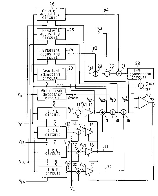
FIG. 1 is a block diagram showing an automatic
tone control circuit for luminance signals. FIG. 2(A) is
a graph showing frequencies of luminance signals, and FIG.
2(B) is a graph showing input-output characteristic of the
automatic tone control circuit. FIG. 3 is a circuit
diagram showing an internal circuit of a known IRE circuit
5 --- 8 in FIG. 1 (IRE:Initial letters of Institute for
Radio Engineers, U.S.). Each of the IRE circuits 5 --- 8
20872~
serves as a brightness frequency detection means. FIG. 4
is a block diagram showing internal circuits of gradient
adjusting circuits 23 --- 26 (illustration of the circuit
25 is omitted) shown in FIG. 1. FIG. 5 is a graph showing
a characteristic of the gradient adJusting circuit shown
in FIG. 4.
In the first place, operation of the automatic
tone control circuit is described. In FIG. 1, a white
peak voltage Vmax contained in an input signal Yin is
extracted by a white-peak detection circuit 9 and is given
to a comparator 27. A range of from O (zero shows the
pedestal level in this description) to the white peak
voltage Vmax is equally divided into four voltage ranges O
~ Vil~ Vil ~ Vi2~ Vi2 - Vi3 and Vi3 - Vi4 by a voltage
dividing circuit, details whereof will be described later.
Voltage signals O and Vi1 are inputted to the IRE circuit
5, and the IRE circuit 5 issues a voltage signal Vj1 which
corresponds to a frequency of appearances of the voltage
from O to Vi1. Voltage signals Vi1 and Vi2 are inputted
to the IRE circuit 6, and the IRE circuit 6 issues a
voltage signal V~2 which corresponds to a frequency of
appearances of the voltage from Vi1 to Vi2. Voltage
signals Vi2 and Vi3 are inputted to the IRE circuit 7, and
the IRE circuit 7 issues a voltage signal V~3 which
corresponds to a frequency of appearances of the voltage
from Vi2 to Vi3. Voltage signals Vi3 and Vi4 are inputted
20872û1
to the IRE circuit 8, and the IRE circuit 8 issues a
voltage signal Vj4 which corresponds to a frequency of
appearances of the voltage from Vi3 to Vi4. These voltage
g als V~1, Vj2, V~3 and Vj4 are added to a voltage
signal VL at adders 11, 14, 17 and 20, thereby resulting
in voltage signals Vk1, Vk2, Vk3 and Vk4, respectively.
This voltage signal VL can be varied by an external
circuit (not shown). Next, the voltage signal Vk1 is
amplified by a gain control circuit 12 and is forwarded to
the gradient adjusting circuit 23 as a voltage signal Vsl.
Also, the voltage signals Vk2, Vk3 and Vk4 are amplified
by gain control circuits 15, 18 and 21, respectively.
Voltage signals amplified by the gain control circuits 12
and 15 are added to each other at an adder 13, and a
resultant voltage signal Vs2 is forwarded to the gradient
adJusting circuit 24. The voltage signal Vs2 and a
voltage signal 71 amplified by the gain control circuit 18
are added to each other at an adder 16, and a resultant
voltage signal Vs3 is forwarded to the gradient adJusting
circuit 25. The voltage signal Vs3 and a voltage signal
72 amplified by the gain control circuit 21 are added to
each other at an adder 19, and a resultant voltage Vs4 is
forwarded to the gradient adjusting circuit 26. The
voltage signal Vs4, which is a final voltage sum, is
compared with the white-peak voltage Vmax at a comparator
27, and a resultant voltage signal 73 of comparison is
20872~1
used to control the gain control circuits 12, 15, 18 and
21. Thus, the voltage signal Vs4 becomes equal to the
white peak voltage Vmax. The gradient adJusting circuits
23, 24, 25 and 26 receive the voltage signals Vsl, Vs2,
Vs3 and Vs4 and issue adJusting currents iS1, iS2, is3 and
is4~ respectively. The ad~usting currents iS1 and iS2 are
added to each other at an adder 29. An output current of
the adder 29 and the adJusting current is3 are added to
each other at an adder 30. Further, an output current of
the adder 30 and the adJusting current is4 are added to
each other at an adder 31. An output current of the adder
31 is inputted to an I - V conversion circuit 28 and is
converted into an adJusting voltage. This adJusting
voltage and the input signal Yin are added to each other
at an adder 32, and a resultant voltage is issued as an
adJusting output signal YoUt~
Next, input-output characteristics of the above-
mentioned automatic tone control circuit is described.
In FIG. 2(A), the frequency of appearance of the voltage
signals in the range (hereinafter is simply referred to as
the frequency of the voltage range) from O to Vi1 is
represented as an integrated value S1; the frequency of
the voltage range from Vi1 to Vi2 is represented as an
integrated value S2; the frequency of the voltage range
from Vi2 to Vi3 is represented as an integrated value S3;
the frequency of the voltage range from Vi3 to Vi4 is
2087201
represented as an integrated value S4. Each of these
integrated values S1, S2, S3 and S4 is added to a constant
voltage VL, thereby resulting in the voltage signals Vk1,
Vk2, Vk3 and Vk4, respectively. Next, in FIG. 2(B), the
voltage signals Vsl, Vs2, Vs3 and Vs4 are obtained by the
following addition of the voltage signals Vk1, Vk2, Vk3
and Vk4:
Vsl = Vk1 = S1 + VL
VS2 = Vkl + Vk2 = S1 + S2 + 2VL
Vs3 = Vkl + Vk2 + Vk3 = S1 + S2 + S3 + 3VL , and
Vs4 = Vkl + Vk2 + Vk3 + Vk4 = S1 + S2 + S3 + S4 + 4VL .
The voltage signal Vs4 becomes equal to the
white-peak voltage Vmax as a result of the aforementioned
feedback control. When the adJusting is made by the
gradient adJusting circuits 23, 24, 25 and 26 (FIG. 1) in
response to the voltage signals Vsl, Vs2, Vs3 and Vs4~ an
input-output characteristic as shown by a line graph in
FIG. 2(B) is obtained. As is apparent from this line
graph, a gradient in a range from the voltage Vi1 to the
voltage Vi2 is made largest because the frequency of this
range has been very high. Thus, tone of image in this
range is stretched, so that images with distinct contrasts
can be obtained.
Next, operation of the IRE circuits 5 --- 8
(FIG. 1), each of which detects a frequency of a specific
brightness, is described concretely with reference to FIG.
- 20~720~
3. In FIG. 3, although an internal circuit is shown only
about the IRE circuit 5, other internal circuits of the
IRE circuits 6, 7 and 8 are similar to the internal
circuit of the IRE circuit 5. The circuit enclosed by a
chain line is the internal circuit of the IRE circuit 5.
The circuit of FIG. 3 consists of diodes Dl, D2,
transistors Ql --- Q20, resistors Rl --- R9, current
sources Il --- I5, a voltage source El and a capacitor Cl.
Frequency of brightness is detected by the IRE circuits 5
--- 8 in response to respective regions of brightness.
When a voltage of the luminance signal (input
signal) Yin is between the voltages ViO(=0) and Vil , a
current Il flows through the collector of the transistor
Q4 by means of the transistors Ql, Q2, Q3 and Q4. The
current Il acts to charge the capacitor Cl by means of a
current mirror consisting of the transistors Q5, Q6 and
the resistors Rl, R2. This means that the frequency of
brightness between the luminance levels (voltage signals)
0 and Vil has been detected. A voltage which appears on
the capacitor Cl is converted to a current by the resistor
R3, and to this current, a current obtained by converting
the external voltage VL by the resistor R4 is added.
Further, a current flows through the collector of the
transistor Q12 by means of a current mirror consisting of
the transistors Q10, Q12 and the resistors R5, R7. The
current flowing through the collector of the transistor
208720~
Q12 enters a differential amplifier consisting of the
transistors Q15 and Q16, together with the similar
currents generated in the IRE circuits 6, 7 and 8. A
current flowing in the transistor Q16 is converted into a
voltage output by the resistor R9, and this output voltage
is compared with the white peak voltage Vwp which is
impressed to the base of the transistor Q20. Thus, the
output voltage of the resistor R9 becomes equal to the
white peak voltage as a result of the feedback control of
the transistors Q17, Q18, Q15 and Q16. Further, the
voltage signal Vsl, which corresponds to the frequency of
brightness, is issued by a current mirror consisting of
the transistors Q12, Q11 and the resistors R7, R6 and a
differential amplifier Q13 and Q14. That is, in FIG.
2(B), the voltage signal Vs4 is equal to the white peak
voltage Vwp, and outputs of the IRE circuits 5, 6, 7 and 8
are equal to the voltage signals Vsl, Vs2, Vs3 and V
respectively.
Next, operation of the gradient adjusting
circuits is described with reference to FIG. 4. A voltage
between the maximum voltage Vmax and the pedestal voltage
V (=0) is divided by resistors Ri1, Ri2, Ri3 (illustr
of Ri3 is omitted because of restriction of the paper
size) and Ri4 into voltage signals Vi1, Vi2, Vi3
(illustration is omitted) and Vi4. These voltage signals
Vi1, Vi2, Vi3 (illustration is omitted), Vi4, output
20B72~1.
setting voltage signals VOl, Vo2, Vo3 (illustration is
omitted), Vo4 and the input signal Yin are inputted to the
gradient adJusting circuits 23 --- 26 (illustration of
the circuit 25 is omitted). Operation of the gradient
adjusting circuits 23, 24 and 26 is described hereafter.
In the gradient ad~usting circuit 24, the input
setting voltage signals Vi1 and Vi2 are inputted to a
ad~usting current generation circuit 61. The ad~usting
current generation circuit 61 issues an ad~usting current
i2, which is in proportion to a differential voltage
between the input voltage Vi1 and Vi2, and its integer
multiples. The current i2 and an adJusting current 2i1 of
the gradient ad~usting circuit 23 are added to each other
by an adding circuit 62 in the gradient adJusting circuit
24, and the adding circuit 62 issues an output current
iT2. The voltage Vi2 having passed through a buffer 63
and the ad~usting current iT2 flowing through an output
resistor 64 give a voltage V2 to an operational amplifier
65. The operational amplifier 65 compares the voltage V2
and the output setting voltage Vo2 and issues a control
signal 66. This control signal 66 is fed-back to the
adJusting current generation circuit 61. The adjusting
current i2 is thus controlled to equalize the voltage V2
with the voltage Vo2. The control signal 66 is also
inputted to the gradient adjusting current generation
circuit 67, so that an ad~usting current 68 is issued from
20872û~
the gradient adjusting current generation circuit 67. The
adJusting current 68 serves to change a gradient of input
versus output at the time when the input signal is within
a range from Vi1 to Vi2. In the similar way to the above,
the gradient adjusting circuit 23 converts the input
voltage Vi1 to the output voltage VOl, and the gradient
adJusting circuit 26 converts the input voltage Vi4 to the
output voltage Vo4.
According to the above-mentioned gradient
adjusting by the gradient adJusting circuits 23 --- 26,
gradient adjusting of the currents i1, i2, i3 and i4 is
carried out to the input voltage signal Vi1, Vi2, Vi3 and
Vi4 as shown in FIG. 5. Thus, a line graph shown by solid
lines is obtained. Hereupon, the output signal voltages
VOl, Vo2, Vo3 and Vo4 correspond to the voltages Vsl, Vs2,
Vs3 and Vs4 in FIG.2(B), respectively.
According to the above-mentioned input-output
characteristic, a luminance range of high frequency (of
appearance) has a large gradient, so that a high contrast
image can be obtained in that range. Further, only by
keeping the maximum output setting voltage (=Vo4) under a
voltage causing the blooming, generation of undesirable
blooming is suppressed. Although in this embodiment the
voltage Vi4 is used as the white peak voltage, another
embodiment may be such that an externally setting voltage
is used as the white peak voltage to obtain high contrast
2087201
images.
In the above-mentioned embodiment, there are
provided "four" gradient adJusting circuits 23 --- 26 and
"four" IRE circuits 5 --- 8. However, the number of each
of the gradient adjusting circuits 23 --- 26 and the IRE
circuits 5 --- 8 may be another integer, e.g., three or
five.
Furthermore, apart from the above-mentioned
embodiment wherein the maximum input signal voltage is
equally divided into plural voltage ranges, another
embodiment may be such that the maximum input signal
voltage is divided into plural voltage ranges which are
irregular in interval of range. An example of this
"irregular ranges" is shown in FIG. 5A. In FIG. 5A, the
input signal voltage range Vi1-Vi2 is twice as long as the
input signal voltage ViO-Vi1 . The number of the circuits
(IRE circuit, gradient adJusting circuit) required to
obtain a characteristic shown by this line graph is three.
An adjusting current "3i1" flows from the first gradient
adjusting circuit to the second gradient adjusting
circuit, and an adjusting current for the range of Vi2-Vi3
is selected "2i1(=3i1-i1)". An adjusting current supplied
from the first gradient adjusting circuit to the second
gradient adjusting circuit is represented by "(3/2)i2".
Thus, a tone control characteristic similar to that shown
in FIG. 5 is obtained even though intervals of the ranges
2087201
are different from each other.
Although the present invention has been
described in terms of the presently preferred embodiments,
it is to be understood that such disclosure is not to be
interpreted as limiting. Various alterations and
modifications will no doubt become apparent to those
skilled in the art after having read the above disclosure.
Accordingly, it is intended that the appended claims be
interpreted as covering all alterations and modifications
as fall within the true spirit and scope of the invention.
16