Note: Descriptions are shown in the official language in which they were submitted.
~ ~ ~ 7 ~ ~ 6
ENCRYPTION SYSTEM FOR DIGITAL CELLULAR COMMUNICATIONS
BACKGROUND OF THE INVENTION
Field of the Invention
The present invention relates to digital cellular
communication systems, and more particularly, to a method
and apparatus for the encryption of data communications
within such a system.
History of the Prior Art
Cellular radio communications is, perhaps, the fastest
growing field in the world-wide telecommunications
industry. Although cellular radio communication systems
comprise only a small fraction of the telecommunications
systems presently in operation, it in widely believed that
this fraction will steadily increase and will represent a
major portion of the entire telecommunications market in
the not too distant future. This belief in grounded in the
inherent limitations of conventional telephone
communications networks which rely primarily on wire
technology to connect subscribers within the network. A
standard household or office telephone, for example, is
connected to a wall outlet, or phone jack, by a telephone
cord of a certain maximum length. Similarly,
CA 02087616 1999-01-21
wires connect the telephone outlet with a local switching
office of the telephone company. A telephone user's
movement is thus restricted not only by the length of the
telephone cord, but also by the availability of an operative
telephone outlet, i.e. an outlet which has been connected
with the local switching office. Indeed, the genesis of
cellular radio system can be attributed, in large part, to
the desire to overcome these restrictions and to afford the
telephone user the freedom to move about or to travel away
lo from his home or office without sacrificing his ability to
communicate effectively with others. In a typical cellular
radio system, the user, or the user's vehicle, carries a
relatively small, wireless device which communicates with a
base station and connects the user to other mobile stations
in the system and to landline parties in the public switched
telephone network (PSTN).
A significant disadvantage of existing cellular radio
communication systems is the ease with which analog radio
transmissions may be intercepted. In particular, some or
all of the communications between the mobile station and the
base station may be monitored, without authorization, simply
by tuning an appropriate electronic receiver to the
frequency or frequencies of the communications. Hence,
anyone with access to such a receiver and an interest in
eavesdropping can violate the privacy of the comml~n; cations
virtually at will and with total impunity. While there have
been efforts to make electronic eavesdropping illegal, the
clandestine nature of such activities generally means that
most, if not all, instances of eavesdropping will go
undetected and, therefore, unpunished and undeterred. The
possibility that a competitor or a foe may decide to "tune
in" to one's seemingly private telephone conversations has
heretofore hindered the proliferation of cellular radio
communication systems and, left unchecked, will continue to
threaten the viability of such system for businesses and
government applications.
CA 02087616 1999-01-21
It has recently become clear that the cellular radio
telecommunications systems of the future will be implemented
using digital rather than analog technology. The switch to
digital is dictated, primarily, by considerations relating
to system speed and capacity. A single analog, or voice,
- radio frequency (RF) channel can accommodate four (4) to six
(6) digital, or data, RF channels. Thus, by digitizing
speech prior to transmission over the voice channel, the
channel capacity and, consequently the overall system
lo capacity, may be increased dramatically without increasing
the bandwidth of the voice channel. As a corollary, the
system is able to handle a substantially greater number of
mobile stations at a significantly lower cost.
Although the switch from analog to digital cellular
radio systems ameliorates somewhat the likelihood of
breeches in the security of communications between the base
station and the mobile station, the risk of electronic
eavesdropping is far from eliminated. A digital receiver
may be constructed which in capable of decoding the digital
signals and generating the original speech. The hardware
may be more complicated and the undertaking more expensive
than in the case of analog transmission, but the possibility
persists that highly personal or sensitive conversations in
a digital cellular radio system may be monitored by a third
party and potentially used to the detriment of the system
users. Moreover, the very possibility of third parties
eavesdropping of a telephone conversation eliminates
cellular telecommlln;cations as a medium for certain
government communications. Certain business users may be
equally sensitive to even the possibility of a security
breech. Thus, to render cellular systems as viable
alternatives to the conventional wireline networks, security
of communications must be available on at least some
circuits.
Various solutions have been proposed to alleviate the
security concerns engendered by radio transmission of
CA 02087616 1999-01-21
confidential data. A known solution, implemented by some
existing communication systems, uses cryptoalgorithms to
encrypt (scramble) digital data into an unintelligible form
prior to transmission. For example, the article entitled
"Cloak and Data" by Rick Grehan in BYTE Magazine, dated June
1990 at pages 311-324, for a general discussion of
cryptographic system. In most systems currently available,
speech is digitized and processed through an encryption
device to produce a communications signal that appears to be
lo random or pseudo-random in nature until it is decrypted at
an authorized receiver. The particular algorithm used by
the encryption device may be a proprietary algorithm or an
algorithm found in the public domain. Further background
for such techniques may be found in the article entitled
"The Mathematics of Public-Key Cryptography" by Martin E.
Hellman in Scientific American dated August 1979 at 146-167.
In 1977, the U.S. National Bureau of Standards
published a cryptoalgorithm defined as the Data Encryption
Standard (DES). See Federal Information Processing
Standards Publication 46 (FIPS PUB 46) of the National
Technical Information Service (1977). The DES method of
encryption utilizes a publicly known mathematical algorithm,
which produces a stream of random numbers, and a data
encryption key consisting of a 64 bit binary word. Digital
data, typically in ASCII format, is transformed into an
apparently random sequence of bits. The encrypted data can
be decrypted pursuant to the standard DES decryption
procedure only if the encryption key, which may be any 64
bit binary word, is also known to the receiver of the
encrypted data. Because the DES encryption and decryption
procedures are publicly known, the security of the key is
crucial to the effective use of DES.
Commercial devices implementing the DES encryption/
decryption procedure are generally in the form of integrated
circuits which accept an a first input the data to be
encrypted and as a second input the 64 bit key. Most such
CA 02087616 1999-01-21
devices operate in a cipher feedback (CFB) mode in which the
encrypted data is provided as a third input to the DES
device so as to prevent the transmission of repetitive
sequences of encrypted data when the data being encrypted
contains repetitive sequences of identical characters. The
chief advantage of CFB encryption of data is self
synchronization of the encrypted signal. However, a major
disadvantage of CFB devices operating over an RF link is the
reduced operational range of the mobile stations caused by
o error multiplication related to receiver sensitivity. That
is, a single error in Transmission of an encrypted data
block produces, on average, half of the bits in the
deciphered data to be in error producing a hugh
magnification of the transmission error rate. Thus, a
mobile station would have to remain within a certain limited
range of a bass station in order to maintain a sufficiently
high signal-to-noise ratio to attempt to avoid erroneous
reception of transmitted data bits. Error multiplication
occurs in CFB mode because erroneously received bits are
continuously fed back to the descryption device until the
error propagates out and the receiver eventually
resynchronizes.
Another known technique for the encryption of data,
which does not suffer from the error multiplication problem
encountered in the CFB mode of operation, is counter
addressing (CA). In the CA mode of operation, a keystream
generator is used to produce a pseudo-random keystream of
bits by processing an encryption key containing a plurality
of key data bits. The keystream is then used by the
encryption device to encrypt the data signal. Typically,
the keystream is added (modulo-2) with the data signal on a
bit-by-bit basis by an exclusive OR (XOR) logic gate to
produce a scrambled binary data signal. The scrambled
signal may be descrambled by adding (modulo 2) to the
scrambled signal an identical keystream generated synchron-
ously by an identical keystream generator that is initial-
CA 02087616 1999-01-21
ized with the same binary encryption key. In this fashion,
the encryption device may be "addressed" by the pseudo-
random counter. Thus, in CA mode, continuous bit synchron-
ization between the scrambler to the descrambler is required
in order to allow proper operation of the descrambler key
generator without necessitating periodic key generator data
transfers. Unfortunately, bit synchronization over an RF
channel in a cellular radio system is very difficult to
maintain due, in large part, to the phenomena of Rayleigh
lo fading which in caused by the movement of the mobile station
through the multi-path interference patterns generated by
reflection from obstacles near the receiving equipment. A
single error bit in transmission through the decryption
circuit out of phase with the encryption circuit and the
output produced at the receiver is meaningless. The CA
technique is generally unsuitable for radio link encryption
which must be more robust against bit transmission errors.
The difficulties attending continuous bit synchroniza-
tion have led to the use of "time-of-day" or "frame number"
driven keystream generators. Such keystream generators may
be synchronized to a time of day counter, i.e. hour, minute
and second, or to a simple number counter and the encryption
and decryption circuits can be sending the current count in
the event one falls out of synchronization with another.
To increase the security of communications in systems
utilizing time-of-day or frame number driven keystream
generators, the value of each bit in the pseudo-random key-
stream is preferably made a function of the values of all
the key bits in the encryption key. In this manner, a
person desiring to descramble the encrypted signal must
"crack" or "break" all of the bits of the encryption key
which may be in the order of a hundred (100) bits or more.
A keystream of this type is generally produced by mathemat-
ically expanding the encryption key word in accordance with
a selected algorithm which incorporates the count of the
time-of-day counter. However, if every bit of the encryp-
CA 02087616 1999-01-21
tion key is to influence every bit in the keystream and if
the keystream is to be added to the data stream bits on a
one-to-one basis, the required number of key word expansion
computations per second is enormous and can readily exceed
the real time computational capability of the system. While
the degree of necessary computations suggests the use of a
supercomputer, the cost of supercomputers for this purpose
in prohibitive. Therefore, a method and apparatus are
needed to achieve the expansion of the keystream with con-
ventional microprocessors and at conventional microprocessorspeeds.
SUMMARY OF THE INVENTION
In one aspect, the invention includes a method of
generating a pseudo-random bit sequence for use in
enciphering digital data in which said bit sequence is a
function of a plurality of selected key bits. The method
includes generating a plurality of multi-bit values each of
which are a function of at least some of said selected key
bits and storing each of said plurality of multi-bit values
in a discrete location in a memory. A sequence of values is
generated in a register by incrementing the present value
contained in the register in response to each cycle of
operation. A sequence of multi-bit values is cyclically
calculated in accordance with a first preselected algorithm
each of which values is a function of at least one of the
multi-bit values stored in said memory and the value con-
tained in said register. The contents of said register is
cyclically reset with a value obtained as a result of each
calculation and a multi-bit keyword is cyclically extracted
which is a function of a value obtained as a result of each
calculation. The multi-bit keywords are sequentially
combined into said pseudo-random bit sequence. In one
embodiment the plurality of multi-bit values generated are
each a function of all of the selected key bits.
CA 02087616 1999-01-21
In another aspect, the present invention includes a
cellular communication system having an encryption subsystem
which includes a keystream generator which uses a secret key
to generate a pseudo-random keystream in two stages. First,
the secret key is expanded in accordance with an algorithm
to produce a look-up table which is stored in memory.
Second, the circuit uses the count of a register along with
the key in combination with the data stored in the look up
table to generate a pseudo-random keystream which is mixed
o with the data before transmission. The system of the
present invention employs a time of day driven counter along
with the data stored in the look-up table and the secret key
and uses them both to generate the keystream. Such counters
in both the transmitter and receiver may be periodically
resynchronized in the event that desynchronization occurs.
In a still further aspect, the present invention
includes a digital cellular communication system in which
the streams of digital data being transmitted and received
by the base station and the mobile units are cryptographi-
cally encoded to provide security of telecommunications.The system incorporates means for adding a pseudo-random
keystream of binary bits to the information carrying digital
signal of each transmitter and receiver in the system to
create stream of digital data to be transmitted and received
within the system. A means for generating the pseudo-random
keystream of binary bits as a function of a plurality of
selected secret key bit includes means for generating a
plurality of multi-bit values each of which are a function
of at least some of the selected key bits along with means
for storing each of said plurality of multi-bit values in a
discrete location in a memory. A means for generating a
sequence of values in a register increments the present
value contained in the register in response to each cycle of
operation. The system also includes a means for cyclically
calculating a sequence of multi-bit values in accordance
with a first preselected algorithm each of which values is a
CA 02087616 1999-01-21
function of at least one of the multi-bit values stored in
the memory and the value contained in the register and a
means for cyclically resetting the contents of the register
with a value obtained as a result of each calculation. A
multi-bit keyword which is a function of a value obtained as
a result of each calculation is cyclically extracted and
combined into the pseudo-random keystream of binary bits
used to cryptographically encode and decode the stream of
digital data to be transmitted and received.
BRIEF DESCRIPTION OF THE DRAWINGS
The present invention will be better understood and its
numerous objects and advantages will become apparent to
those skilled in the art by reference to the following
drawings in which:
FIG. 1 is a pictorial representation of a cellular
radio communications system including a mobile switching
center, a plurality of base stations and a plurality of
mobile stations;
FIG. 2 is a schematic block diagram of mobile station
equipment used in accordance with one embodiment of the
system of the present invention;
FIG. 3 in a schematic block diagram of base station
equipment used in accordance with one embodiment of the
system of the present invention;
FIG. 4 in a schematic block diagram of a prior art
keystream generator;
FIG. 5 is a schematic block diagram of a keystream
generator circuit of an encryption system constructed in
accordance with the present invention; and
FIG. 6 is a partial schematic block diagram of a second
expansion stage of the keystream generator shown in FIG. 5.
DETAILED DESCRIPTION OF THE PREFERRED EMBODIMENT
Referring first to FIG. 1, there is illustrated therein
a conventional cellular radio communications system of a
CA 02087616 1999-01-21
type to which the present invention generally pertains. In
FIG. 1, an arbitrary geographic area may be seen divided
into a plurality of contiguous radio coverage areas, or
cells, C1-C10. While the system of FIG. 1 is shown to
include only 10 cells, it should be clearly understood that,
in practice, the number of cells may be much larger.
Associated with and located within each of the cells
C1-C10 is a base station designated as a corresponding one
of a plurality of base stations B1-B10. Each of the base
lo stations B1-B10 includes a transmitter, a receiver and
controller as is well known in the art. In FIG. 1, the base
stations B1-B10 are located at the center of the cells
C1-C10, respectively, and are equipped with omni-directional
antennas. However, in other configurations of the cellular
radio system, the base stations B1-B10 may be located near
the periphery, or otherwise away from the centers of the
cells C1-C10 and may illuminate the cells C1-C10 with radio
signals either omni-directionally or directionally.
Therefore, the representation of the cellular radio system
of FIG. 1 is for purposes of illustration only and is not
intended as a limitation on the possible implementations of
the cellular radio system.
With continuing reference to FIG. 1, a plurality of
mobile stations M1-M10 may be found within the cells Cl-C10.
Again, only ten mobile stations are shown in FIG. 1 but it
should be understood that the actual number of mobile
stations may be much larger in practice and will invariably
exceed the number of base stations. Moreover, while none of
the mobile stations M1-M10 may be found in some of the cells
C1-C10, the presence or absence of the mobile stations
M1-M10 in any particular one of the cells C1-C10 should be
understood to depend, in practice, on the individual desires
of each of the mobile stations M1-M10 who may roam from one
location in a cell to another or from one cell to an
adjacent or neighboring cell.
CA 02087616 1999-01-21
Each of the mobile stations M1-M10 is capable of initi-
ating or receiving a telephone call through one or more of
the base stations B1-B10 and a mobile switching center MSC.
The mobile switching center MSC is connected by communica-
tions links, e.g. cables, to each of the illustrative base
stations B1-B10 and to the fixed public switching telephone
network (PSTN), not shown, or a similar fixed network which
may include an integrated system digital network (ISDN)
facility. The relevant connections between the mobile
lo switching center MSC and the base stations B1-B10, or
between the mobile switching center MSC and the PSTN or
ISDN, are not completely shown in FIG. 1 but are well known
to those of ordinary skill in the art. Similarly, it is
also known to include more than one mobile switching center
in a cellular radio system and to connect each additional
mobile switching center to a different group of base
stations and to other mobile switching centers via cable or
radio links.
Each of the cells C1-C10 is allocated a plurality of
voice or speech channels and at least one access or control
channel. The control channel is used to control or super-
vise the operation of mobile stations by means of informa-
tion transmitted to and received from those units. Such
information may include incoming call signals, outgoing call
signals, page signals, page response signals, location
registration signals, voice channel assignments, maintenance
instructions and "handoff" instructions as a mobile station
travels out of the radio coverage of one cell and into the
radio coverage of another cell. The control or voice chan-
nels may operate either in an analog or a digital mode or acombination thereof. In the digital mode, analog messages,
such as voice or control signals, are converted to digital
signal representations prior to transmission over the RF
channel. Purely data messages, such as those generated by
computers or by digitized voice devices, may be formatted
and transmitted directly over a digital channel.
11
CA 02087616 1999-01-21
In a cellular radio system using time division multi-
plexing (TDM), a plurality of digital channels may share a
common RF channel. The RF channel is divided into a series
of "time slots", each containing a burst of information from
a different data source and separated by guard time from one
another, and the time slots are grouped into "frames" as is
well known in the art. The number of time slots per frame
varies depending on the bandwidth of the digital channels
sought to be accommodated by the RF channel. The frame may,
lo for example, consist of three (3) time slots, each of which
is allocated to a digital channel. Thus, the RF channel
will accommodate three digital channels. In one embodiment
of the present invention discussed herein, a frame is
designated to comprise three time slots. However, the
teachings of the present invention should be clearly under-
stood to be equally applicable to a cellular radio system
utilizing any number of time slots per frame.
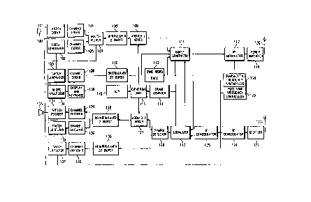
Referring next to FIG. 2, there is shown therein a
schematic block diagram of the mobile station equipment
which are used in accordance with one embodiment of the
present invention. The equipment illustrated in FIG. 2 may
be used for communication over digital channels. A voice
signal detected by a microphone 100 and destined for trans-
mission by the mobile station in provided as input to a
speech coder 101 which converts the analog voice signal into
a digital data bit stream. The data bit stream is then
divided into data packets or messages in accordance with the
time division multiple access (TDMA) technique of digital
communications. A fast associated control channel (FACCH)
generator 102 exchanges control or supervisory messages with
a base station in the cellular radio system. The conven-
tional FACCH generator operates in a "blank and burst"
fashion whereby a user frame of data is muted and the con-
trol message generated by the FACCH generator 102 is trans-
mitted instead at a fast rate.
CA 02087616 1999-01-21
In contrast to the blank and burst operation of the
FACCH generator 102, a slow associated control channel
(SACCH) generator 103 continuously exchanges control
messages with the base station. The output of the SACCH
generator is assigned a fixed length byte, e.g. 12 bits, and
included as a part of each time slot in the message train
(frames). Channel coders 104, 105, 106 are connected to the
speech coder 101, FACCH generator 102 and SACCH generator
103, respectively. Each of the channel coders 104, 105, 106
o performs error detection and recovery by manipulating
incoming data using the techniques of convolutional encod-
ing, which protects important data bits in the speech code,
and cyclic redundancy check (CRC), wherein the most signifi-
cant bits in the speech coder frame, e.g., 12 bits, are used
for computing a 7 bit error check.
Referring again to FIG. 2, the channel coders 104, 105
are connected to a multiplexer 107 which is used for time
division multiplexing of the digitized voice messages with
the FACCH supervisory messages. The output of the multi-
plexer 107 is coupled to a 2-burst interleaver 108 which
divides each data message to be transmitted by the mobile
station (for example, a message containing 260 bits) into
two equal but separate parts (each part containing 130 bits)
arranged in two consecutive time slots. In this manner, the
deteriorative effects of Rayleigh fading may be signifi-
cantly reduced. The output of the 2-burst interleaver 108
is provided an input to a modulo-2 adder 109 where the data
to be transmitted in ciphered on a bit-by-bit basis by
logical modulo-2 addition with a pseudo-random keystream
which is generated in accordance with the system of the
present invention described below.
The output of the channel coder 106 is provided as
input to a 22-burst interleaver 110. The 22-burst inter-
leaver 110 divides the SACCH data into 22 consecutive time
slots, each occupied by a byte consisting of 12 bits of
control information. The interleaved SACCH data forms one
13
CA 020876l6 l999-0l-2l
of the inputs to a burst generator 111. Another input to
the burst generator 111 in provided by the output of the
modulo-2 adder 109. The burst generator 111 produces
"message bursts" of data, each consisting of a time slot
identifier ~TI), a digital voice color code (DVCC), control
or supervisory information and the data to be transmitted,
as further explained below.
Transmitted in each of the time slots in a frame is a
time slot identifier (TI), which is used for time slot
lo identification and receiver synchronization, and a digital
voice color code (DVCC), which ensures that the proper RF
channel is being decoded. In the exemplary frame of the
present invention, a set of three different 28-bit TIs is
defined, one for each time slot while an identical 8-bit
DVCC in transmitted in each of the three time slots. The TI
and DVCC are provided in the mobile station by a sync word/
DVCC generator 112 connected to the burst generator 111 as
shown in FIG. 2. The burst generator 111 combines the out-
puts of the modulo-2 adder 109, the 22-burst interleaver 110
and the sync word/DVCC generator 112 to produce a series of
message bursts, each comprised of data (260 bits), SACCH
information (12 bits), TI (28 bits), coded DVCC (12 bits)
and 12 delimiter bits for a total of 324 bits which are
integrated according to the time slot format specified by
the EIA/TIA IS-54 standard.
Each of the message bursts in transmitted in one of the
three time slots included in a frame as discussed herein-
above. The burst generator 111 is connected to an equalizer
113 which provides the timing needed to synchronize the
transmission of one time slot with the transmission of the
other two time slots. The equalizer 113 detects timing
signals sent from the base station (master) to the mobile
station (slave) and synchronizes the burst generator 111
accordingly. The equalizer 113 may also be used for
checking the values of the TI and the DVCC. The burst
generator 111 is also connected to a 20ms frame counter 114
14
CA 02087616 1999-01-21
which is used to update a ciphering code that is applied by
the mobile station every 20ms, i.e., once for every trans-
mitted frame. The ciphering code is generated by a
ciphering unit 115 with the use of a mathematical algorithm
and under the control of a key 116 which is unique to each
mobile station. The algorithm may be used to generate a
pseudo-random keystream in accordance with the present
invention and an discussed further below.
The message bursts produced by the burst generator 110
lo are provided as input to an RF modulator 117. The RF modu-
lator 117 in used for modulating a carrier frequency
according to the ~/4-DQPSK technique (~/4 shifted, differ-
entially encoded quadrature phase shift key). The use of
this technique implies that the information to be trans-
mitted by the mobile station is differentially encoded,
i.e., two bit symbols are transmitted as 4 possible changes
in phase: + or - ~/4 and + or - 3 ~/3. The carrier fre-
quency for the selected transmitting channel is supplied tothe RF modulator 117 by a transmitting frequency synthesizer
118. The burst modulated carrier signal output of the RF
modulator 117 is amplified by a power amplifier ll9 and then
transmitted to the base station through an antenna 120.
The mobile station receives burst modulated signals
from the base station through an antenna 121 connected to a
receiver 122. A receiver carrier frequency for the selected
receiving channel in generated by a receiving frequency
synthesizer 123 and supplied to an RF demodulator 124. The
RF demodulator 124 is used to demodulate the received
carrier signal into an intermediate frequency signal. The
intermediate frequency signal is then demodulated further by
an IF demodulator 125 which recovers the original digital
information as it existed prior to ~/4-DQPSK modulation.
The digital information is then passed through the equalizer
113 to a symbol detector 126 which converts the two-bit
CA 02087616 1999-01-21
symbol format of the digital data provided by the equalizer
114 to a single bit data stream.
The symbol detector 126 produces two distinct outputs:
a first output, comprised of digitized speech data and FACCH
data, and a second output, comprised of SACCH data. The
first output is supplied to a modulo-2 adder 127 which is
connected to a 2-burst deinterleaver 128. The modulo-2
adder 127 is connected to the ciphering unit 115 and is used
to decipher the encrypted transmitted data by subtracting on
lo a bit-by-bit basis the same pseudo-random keystream used by
the transmitter in the base station to encrypt the data.
The modulo-2 adder 127 and the 2-burst deinterleaver 128
reconstruct the speech/SACCH data by assembling and
rearranging information derived from two consecutive frames
of the digital data. The 2-burst deinterleaver 128 is
coupled to two channel decoders 129, 130 which decode the
convolutionally encoded speech/SACCH data using the reverse
process of coding and check the cyclic redundancy check
(CRC) bits to determine if any error has occurred. The
channel decoders 129, 130 detect distinctions between the
speech data on the one hand, and any SACCH data on the
other, and route the speech data and the SACCH data to a
speech decoder 131 and an SACCH detector 132, respectively.
The speech decoder 131 processes the speech data supplied by
the channel decoder 129 in accordance with a speech coder
algorithm, e.g. VSELP, and generates an analog signal
representative of the speech signal transmitted by the base
station and received by the mobile station. A filtering
technique may then be used to enhance the quality of the
analog signal prior to broadcast by a speaker 133. Any
SACCH messages detected by the SACCH detector 132 are
forwarded to a microprocessor 134.
The second output of the symbol detector 126 (SACCH
data) is supplied to a 22-burst deinterleaver 135. The 22-
burst interleaver 135 reassembles and rearranges the SACCH
data which is spread over 22 consecutive frames. The output
16
CA 020876l6 l999-0l-2l
of the 22-burst deinterleaver 135 is provided as input to a
channel decoder 136. SACCH messages are detected by an
SACCH detector 137 and the control information is
transferred to the microprocessor 134.
The microprocessor 134 controls the activities of the
mobile station and communications between the mobile station
and the base station. Decisions are made by the
microprocessor 134 in accordance with messages received from
the base station and measurements performed by the mobile
lo station. The microprocessor 134 is also provided with a
terminal keyboard input and display output unit 138. The
keyboard and display unit 138 allows the mobile station user
to exchange information with the base station.
Referring next to FIG. 3, there is shown a schematic
block diagram of the base station equipment which are used
in accordance with the present invention. A comparison of
the mobile station equipment shown in FIG. 2 with the base
station equipment shown in FIG. 3 demonstrates that much of
the equipment used by the mobile station and the base
station are substantially identical in construction and
function. Such identical equipment are, for the sake of
convenience and consistency, designated with the same
reference numerals in FIG. 3 as those used in connection
with FIG. 2, but are differentiated by the addition of a
prime (') in FIG. 3.
There are, however, some minor differences between the
mobile station and the base station equipment. For
instance, the base station has, not just one but, two recei-
ving antennas 121'. Associated with each of the receiving
antennas 121' are a receiver 122', an RF demodulator 124',
and an IF demodulator 125'. Furthermore, the base station
includes a programmable frequency combiner 118A' which is
connected to a transmitting frequency synthesizer 118'. The
frequency combiner 118A' and the transmitting frequency syn-
thesizer 118' carry out the selection of the RF channels to
be used by the base station according to the appllcable
17
CA 020876l6 l999-0l-2l
cellular frequency reuse plan. The base station, however,
does not include a user keyboard and display unit similar to
the user keyboard and display unit 138 present in the mobile
station. It does however include a signal level meter 100'
connected to measure the signal received from each of the
two receivers 122' and to provide an output to the micro-
processor 134'. Other differences in equipment between the
mobile station the base station may exist which are well
known in the art.
The discussion thus far has focused on the operational
environment of the system of the present invention. A
specific description of a particular embodiment of the
present invention follows. As disclosed above and used
hereinafter, the term "keystream" means a pseudo-random
sequence of binary bits or blocks of bits used to encipher a
digitally encoded message or data signal prior to
transmission or storage in a medium which is susceptible to
unauthorized access, e.g., an RF channel. A "keystream
generator" means a device which generates a keystream by
processing a secret key comprised of a plurality of bits.
Encryption may be simply performed by a modulo-2 addition of
the keystream to the data to be encrypted. Similarly,
decryption may be performed by a modulo-2 subtraction of an
identical copy of the keystream from the encrypted data.
Generally speaking, the keystream generator provides a
mechanism, represented by elements 115 and 115' of Figs. 2
and 3, respectively, for expanding a relatively small number
of secret bits, i.e., the secret key, represented by
elements 116 and 116', into a such larger number of
keystream bits which are then used to encrypt data messages
prior to transmission (or storage). To decrypt an encoded
message, the receiver must "know" the index to the keystream
bits used to encrypt the message. In other words, the
receiver must not only have the same keystream generator and
generate the same keystream bits as the transmitter, but
also, the receiver keystream generator must be operated in
18
CA 02087616 1999-01-21
synchronism with the transmitter keystream generator if the
message is to be properly decoded. Synchronization is
normally achieved by periodically transmitting from the
encoding system to the decoding system the contents of every
internal memory device, such an bit, block or message
counters, which participate in the generation of the
keystream bits. Synchronization may be simplified, however,
by using arithmetic bit block counters, such as binary
counters, and incrementing those counters by a certain
lo amount each time a new block of keystream bits is produced.
Such counters may form a part of a real-time, i.e. hours,
minutes and seconds, clock chain. A keystream generator
- 18a -
~ ~ ~ 7 ~ ~ ~
.._
relying on the latter type of counters is known as the
"time-of-day" driven keystream generator to which reference
was made hereinabove.
The system of the present invention, an hereinafter
described in detail, is directed to the efficient
implementation of an effective encryption system which may
be used, for example, to secure digital communication over
RF channels in a cellular telecommunications system. The
encryption system includes a keystream generator which
o produces a high number of keystream bits per second by
performing a large number of boolean operations per second
on a plurality of key bits contained in a secret key. The
keystream generator of the present invention may be
implemented with an integrated circuit having a simple
microprocessor architecture.
Referring now to FIG. 4, a schematic block diagram of
a prior art keystream generator may now be seen. An
optional block counter 201 provides a first multi-bit input
to a combinatorial logic circuit 202. A plurality of one-
bit memory elements, or flip-flops, ml, m2, m3... mn
provides a second multi-bit input to the combinatorial
logic circuit 202. A portion of the output of the
combinatorial logic circuit 202, consisting of one-bit
outputs dl, d2, d3... dn, is fed back to the flip-flops ml-
mn. The outputs dl-dn become the next state of the flip-
flops ml-mn, respectively, after each clock pulse in a
series of bit clock input pulses 203 supplied to the flip-
flops ml-mn. By suitable construction of the combinatorial
logic circuit 202, the flip-flops ml-mn may be arranged to
form a straight binary counter, a linear feedback shift
register executing a maximum length sequence, or any other
form of linear or non-
-- 19 --
~ :'
CA 02087616 1999-01-21
linear sequential counters. In any event, each of the
states of the flip-flops ml-mn and the state of the block
counter 201 at the receiver end must be made equal to the
states of the corresponding elements at the transmitter end.
A reset or synchronization mechanism 204 is used to
synchronize the receiver with the transmitter.
With continuing reference to FIG. 4, a plurality of
secret key bits kl, k2, k3... kn, forms a third multi-bit
input to the combinatorial logic circuit 202. The number n
of secret key bits is usually in the region of a hundred
bits plus or minus (+/-) a factor of 2. It is desirable
that each of the secret key bits kl-kn should, at a minimum,
have the potential of affecting each of the bits in the
keystream. Otherwise, an eavesdropper would need to break
only a small subset of the secret key bits kl-kn in order to
decipher and monitor the encrypted data. The risk of
unauthorized interception, however, may be considerably
reduced if the value (logical state) of each bit in the
keystream is made to depend not only on the value of a
particular secret key bit, but also on the value of all
other secret key bits as well as the state of the block
counter 201 and other internal memory states. Heretofore,
the establishment of such a dependence would have entailed a
prohibitive number of boolean operations. Assume, for
example, that the secret key is composed of one hundred
(100) secret key bits. If each of these secret key bits is
to influence every bit in the keystream, a total of one
hundred (100) combinatorial operations per keystream bit
would be required. Thus, to produce ten thousand (10,000)
keystream bits, a total of one million (1,000,000)
combinatorial operations would be required and the number
would be even greater if each keystream bit was also made to
depend on one or more internal memory states. One of the
objectives of the present invention is to significantly
reduce the required number of combinatorial operations per
CA 02087616 1999-01-21
keystream bit while maintaining the dependence of each
keystream bit on every one of the secret key bits.
According to the present invention, the production of
many thousands of pseudo-random keystream bits from, for
example, a (hundred) 100 secret key bits may be viewed as a
multi-stage expansion process. A plurality of expansion
stages are cascaded together, each having a successively
smaller expansion ratio. Expansion by the first stage is
performed less frequently than by subsequent stages in order
lo to minimize the number of required logical (boolean)
operations per keystream bit. Additionally, the first
expansion stage is constructed to provide a plurality of
output bits which is highly dependent on the secret key
bits, further reducing the number of logical operations
which must be performed by the subsequent stages.
Referring next to FIG. 5, a schematic block diagram of
a keystream generator system constructed in accordance with
the teachings of the present invention may now be seen. A
plurality of secret key bits kl, k2, k3... are provided as
input to a first stage expansion 205. The key bits kl, k2,
k3... may include some, but preferably all, of the secret
key bits kl, k2, k3... kn. Additional, or optional, inputs
to the first stage expansion 205 may include the outputs of
a message counter, a block counter, a date-time stamp
representing the time or block count number at the start of
a frame, or other variable outputs which may be synchronized
by the sender and receiver. Any internal memory output
which varies slowly with time may be used as an input to the
first stage expansion 205. A slow changing input is desired
because the first stage expansion 205 should be performed
infrequently, e.g., once per message.
The first stage expansion 205 generates an expanded
output which is considerably larger in size than the number
of secret key bits kl, k2, k3... The expanded output is
stored in a memory device 206 which is accessed by a
combinatorial logic circuit 207. The combinatorial logic
21
CA 02087616 1999-01-21
207 performs a second stage expansion as more fully set
forth below. The output of a counter or register 208 forms
an input to the combinatorial logic 207. The register 208
is initialized to a new starting state prior to the
generation of each block of keystream bits. An initial
value generator 209 provides the starting state for the
register 208. The starting state, which will be different
for each particular block of keystream bits, is a function
of the block number of the particular block and, possibly,
also a function of some subset of the secret key bits kl-kn.
A first output 210 of the combinatorial logic 207 is
fed back to the register 208. The output 210 becomes the
new state of the register 208 after each cycle of operation.
A second output 211 of the combinatorial logic 207 forms the
keystream bits which are to be mixed with the data stream as
shown in FIGS. 2 and 3, above. The number of keystream bits
produced per cycle at the output 211 may be any multiple of
2, i.e., 8, 16, 32, 56, etc. Such bits are collectively
referred to as a "keyword". Some or all of the keywords
produced at the output 211 prior to reinitialization of the
register 208 are grouped into a keyblock 212. The keyblock
212 may, for example, consist of all the keywords produced
in every cycle, or in every other cycle, preceding
reinitialization of the register 208.
It will be appreciated by those skilled in the art that
a conventional implementation of the keystream generator
system depicted in FIG. 5 and discussed above might require
a host of complex combinatorial logic circuits which, if
realized separately by interconnecting a plurality of logic
gates, i.e., AND, OR etc., would amount to a large and
costly chip, useful only for a very specific application.
An arithmetic and logic unit (ALU), on the other hand, is a
standard component of a variety of small, low-cost and
multi-purpose microprocessors. The present invention
provides a means for realizing all of the required
combinatorial logic functions with the use of such an ALU.
22
CA 02087616 1999-01-21
The conventional ALU, operating under the control of a
program, can perform the combinatorial functions ADD,
SUBTRACT, BITWISE EXCLUSIVE OR, AND, OR between any two 8-
bit or 16-bit binary words. If the ALU is used to
sequentially implement all of the boolean functions required
in the device of FIG. 5, the ALU operating speed, measured
in terms of the number of complete cycles per second that
may be executed, would be substantially reduced. The multi-
stage expansion used in the present invention, however,
0 prevents such excessive reduction of ALU speed by minimizing
the number of program instructions, i.e., instances of ALU
utilization, per cycle for the most frequently executed
combinatorial logic 207 through the infrequently periodic
calculation of a large number of key-dependent functions in
the first stage expansion 205. By the word "large" in the
preceding sentence, is meant, for example, an order of
magnitude larger than the number n of secret key bits.
Once the register 208 is initialized with a starting
value, the combinatorial logic 207 will generate a stream of
keywords at the output 211 and will continue to generate
additional keywords each time the register 208 is reloaded
with the feedback value at the output 210. Difficulties may
arise, however, which can undermine the integrity of the
keyword generation process. If, for example, the contents
of the register 208 ever return to their initial value, the
sequence of the keywords generated theretofore will repeat
again. Similarity, if the contents of the register 208
return to a value (not necessarily the initial value)
previously encountered in the generation of the current
keyblock, the system in said to be "short cycling". For
reasons alluded to earlier, e.g., the ease of unauthorized
deciphering, it is undesirable that the sequence of keywords
should begin to repeat, or that short cycling should occur,
within the generation of a single keyblock. Moreover, if
the contents of the register 208 at some point, say after
the m'th keyword is generated, become equal to some value
23
CA 02087616 1999-01-21
which existed or will exist after the m'th keyword during
the generation of another keyblock, the two keyblocks will,
from that point on, be identical--also an undesirable
occurrence.
Hence, the combinatorial logic 207 and the associated
register 208 (the "combinatorial logic/register
combination"), when operated successively a number of times,
should (i) not produce cycles shorter than the number of
keywords per block; and (ii) produce a unique keyword
lo sequence for every unique starting state of the register
208. To meet the latter requirement, no two different
starting states should be capable of converging to the same
state. Furthermore, both of the foregoing requirements
should apply regardless of the contents of the memory 206.
As explained in more detail below, the present invention
alleviates these concerns and enhances the integrity of the
keyword generation process.
When the state transition diagram of the combinatorial
logic/register combination has converging forks, the
combination may not be run in reverse through such a fork
because of the ambiguity about which path to take.
Therefore, if a process for operating the combination can be
shown to be unambiguous or reversible, it in proof that
converging forks do not exist in the state transition
diagram. Such a process is described and discussed below.
Referring next to FIG. 6, a partial schematic block
diagram of the second expansion stage of the keystream
generator shown in FIG. 5 may now be seen. The register 208
of FIG. 5 has been divided into three byte-length registers
208A, 208B, 208C in FIG. 6. The registers 208A, 208B, 208C
may be, for example, 8-bit registers. Following
initialization of the registers 208A, 208B, and 208C, new
state values are calculated from the following formulas:
(1) A' = A # ~K(B) + K(C)]
(2) B' = B # R(A)
(3) C' = C + 1
24
CA 02087616 1999-01-21
where,
A' is the new state value for the register 208A;
B' is the new state value for the register 208B;
C' is the new state value for the register 208C;
A is the current state value for the register 208A;
B is the current state value for the register 208B;
C is the current state value for the register 208C;
+ means word-length modulo additions, for example,
byte wide modulo-256 additions;~0 # means + (as defined above) or bitwise exclusive OR
(XOR);
K(B) is the value K located at address B of the memory
206 shown in FIG. 5;
K(C) is the value K located at address C of the memory
206 shown in FIG. 5;
Note: Each of the values K stored in the memory 206 has
been previously calculated to be a complex function of all
the secret keybits by the first stage expansion 205 shown in
FIG. 5.~0 R(A) is the value located at address A in a fixed look-up
table R. Alternatively, the bits of A are supplied as
inputs to a combinatorial logic block which will
produce an output R. The look-up table R, or
alternatively, the combinatorial logic block should
provide a number of output bits greater or equal to the
word length of A and less or equal to the word length
of B. In the case where A and B are both 8-bit bytes,
for example, R will also be an 8-bit byte and the look-
up table R will contain 256 values.~0
The value R should have a 1:1 mapping from input to
output; that is, each possible state of the input bits
should map to a unique output value. This ensures that the
R function is reversible which, in turn, ensures that the
whole process may be reversed by means of the following
relationships:
CA 02087616 1999-01-21
(1) C = C - 1
(2) B = B ## R'(A)
(3) A = A ## [K(B) + K(C)]
where,
- means word-length modulo subtraction;
## means the inverse operation of #, i.e., either-
(as defined above) or bitwise XOR; and
R' is the inverse of the 1:1 look-up table, or the
combinatorial logic, R.
This reversibility demonstrates that there are no
converging forks in the state transition diagram of the
combinatorial logic/register combination and, hence,
guarantees that every starting state will produce a unique
sequence of keywords. Furthermore, the process guarantees a
minimum cycle length, since C is incremented only by 1 and
will not return to its initial value until after 2w
iterations, where w is the word length used. For example,
if all of the values A, B, C, R and K are 8-bit bytes, the
minimum cycle length will be 256. If, upon every iteration
(cycle), a keyword (byte) is extracted, a total of 256 bytes
may be extracted without the danger of premature repetition
of the sequence. If, on the other hand, the keyword is
extracted every other iteration, a total of 128 keywords may
be extracted without premature repetition of the sequence.
By the word "extracted" in the preceding two sentences, is
meant the collection and placement of keywords into a
keyblock such as the keyblock 212 in FIG. 5. A particular
method of keyword extraction which may be used in the
present invention in described immediately below.
In connection with FIG. 6, a process was described for
computing the outputs 210 of the combinatorial logic 207
which are fed back to the register 208. Generally speaking,
any one of the intermediate quantities A, B or C may be
directly extracted and used as a keyword on each iteration.
Letting S = (A, B, C) stand for the current state of the
combinatorial logic/register combination, the combination
26
CA 02087616 1999-01-21
will transit through a sequence of states S0, S1, S2, S3,
S4, S5, S6, S7... following initialization to S0. If,
however, in the computation of a subsequent keyblock the
register 208 is initialized, for example, to S2, the
resulting sequence S2, S3, S4, S5, S6, S7... will be
identical to the first sequence but shifted by two keywords
(S0, S1). Therefore, if a value A, B, or C from a state S
is directly used as a keyword, such an identity may appear
between different keyblocks. To prevent this, the system of
0 the present invention modifies each of the values extracted
in accordance with the value's position in the keyblock so
that if the same value is extracted to a different keyword
position in another block, a different keyword will result.
An exemplary method for achieving the latter objective is
set forth below.
Let N be the number of keywords in the keyblock
currently being computed and S = (A, B, C) be the current
state of the register 208 in the iteration during which the
keyword N is to be extracted. The value of the keyword W(N)
may be calculated as follows:
W(N) = B +' K[A + N]
where,
+ means XOR;
+' means either + (as defined immediately above) or
word length-modulo addition.
Other suitable exemplary methods for keyword extraction
may include the following:
W(N) = B + K[R(A + N)] or
W(N) = R[A + N] + K[B + N] and so forth.
While the precise nature of the keyword extraction
method is not material to the operation of the present
invention, it is recommended that, to obtain the best
cryptographic properties in accordance with the system of
the present invention, the values of the keywords extracted
should be a function of their respective positions within a
keyblock.
27
CA 02087616 1999-01-21
As can be seen from the above description of various
embodiments of the system of the invention, there is
included a method and means for reducing the amount of
specific logic hardware required to generate a pseudo-random
bit sequence which is a function of, among other parameters,
a selected number of secret key bits and which is to be used
enciphering a stream of digital information. The system
involves timesharing under program control a general purpose
Arithmetic and Logic Unit (ALU) of the type commonly found
lo in conventional microprocessor integrated circuits chips.
The system minimizes the number of ALU operations needed per
output bit, for a selected degree of complexity of
dependance upon key bits, by the precalculation and storage
in memory of a set of digital values larger in number than
the number of original input key bits. Each one of the
stored digital values is a different and complex logical
function of the key bits, and optionally also a function of
other parameters. The digital values stored in memory are
used as a look-up table by a subsequent calculation stage
which is executed a large number of times to produce a large
number of pseudo-random output bits.
It should be understood that the pseudo-random bit
sequence generator of the system of the present invention
may use many different variables, along with the secret key
bits, in the precalculation of digital values. For example,
the following parameters may be used for this purpose:
message number, sender's identification code or telephone
number, intended receiving correspondent's identification
code or telephone number, time-of-day, date, a counter value
at the start of the message, call number, random number
exchanged between the correspondents, or any other bits or
quantity upon which the sender and the receiver(s) have a
means of agreeing.
Based upon the foregoing discussion it should be clear
that the system uses the precalculated and stored digital
values by first initializing the state of a number of flip-
28
CA 02087616 1999-01-21
flops or register stages that form the inputs to a
combinatorial logic circuit which computes the next state of
a set of values. The computed values are then transferred
into the register stages, upon completion of the next-state
computations, and those new values are used as a new
starting state by the combinatorial logic to iteratively
generate a succession of additional states the logical
values of which is further combined to form the desired
output pseudo-random bit sequence.
o The flip-flops or register stages are initialized to a
value which can dependant upon at least an identification
code or block count of the block of pseudo-random bits
currently being generated and, optionally, upon other
parameters agreed between the correspondents, such as some
or all of the secret key bits. Such dependance of the
initialization value, preferably, but not necessarily,
produces a unique initial register state for each unique
block identification number.
The sub-group of bits generated upon each transition of
20 the register/combinatorial logic state machine between each
successive state is a function not only of the register
states but also of position of the sub-group within the
pseudo-random bit block currently being generated by the
machine. The state machine is guaranteed to produce a
unique sequence of pseudo-random bits in a particular block
for each different block identification code or block number
used to initialize the state machine's register stages, by
ensuring that different starting stages cannot on some
subsequent iteration lead to the same intermediate state.
It can also be seen from the forgoing description that
the state machine of the present invention, which is
composed of a number of register stages connected to a
combinatorial logic circuit and which employs a key-
dependant look-up table having arbitrary contents, exhibits
cyclic behavior on successive iterations. A guaranteed
minimum cycle length is ensured by providing that a sub-
29
CA 02087616 1999-01-21
group of the register stages execute a defined cyclic
sequence such as, for example, a regular incrementing binary
count sequence of at least a minimum length. The state
machine also includes within it one or more fixed look-up
tables, on which the correspondents have agreed, and which
have a 1:1 mapping property from input address to output
address value and are therefore invertible.
The foregoing description shown only certain particular
embodiments of the present invention. However, those
lo skilled in the art will recognize that many modifications
and variations may be made without departing substantially
from the spirit and scope of the present invention.
Accordingly, it should be clearly understood that the form
of the invention described herein is exemplary only and is
not intended as a limitation on the scope of the invention
as defined in the following claims.