Note: Descriptions are shown in the official language in which they were submitted.
W~ 92/02945 PCT/U591/03307
1
-1-
CHANNEL ELECTRON MULTIPLIER PHOT TUBE
Backcrround of the Invention
This invention relates to an improved
channel electron multiplier made from a monolithic
ceramic body and a method of making same. In
particular it relates to a channel electron
multiplier wherein said channel provides a preferably
three dimensional, curved conduit for increased
electron/wall collisions and for a device of smaller
dimension, particularly when longer channel length is
required. The invention further relates to
phototubes employing those and similar electron
multipliers, and to placement of the photaemission .
element relative to both the faceplate and passageway
surface.
Electron multipliers are typically employed
in multiplier phototubes where they serve as
amplifiers of the current emitted from a photocathode
when impinged upon by a light signal. Tn such prior
art multiplier phototube devices, the photocathode,
electron multiplier and other functional elements are
WO 92/02946 1'CT/US91/0330?..
~~~U~~~ -2
enclosed as discrete elements in a surrounding vacuum
envelope, for example, an envelope made of glass.
The vacuum environment inside the envelope is
essentially stable and is controlled during the -
manufacture of the tube for optimum operational
performance. The electron multiplier in this type cf
application generally employs a discrete metal alloy
dynode such as formed from beryllium-copper or
silver-magnesium alloys. Generally, the electron
multiplier must be mounted as a discrete element
within the envelope, and, as a result, the phototube
device is susceptible to damage due to vibration and
shock. Further, since the multiplier is wholly
within the vacuum envelope, there is relatively poor
thermal coupling between the hot dynode surfaces of
the multiplier and the ambient external environment
of the phototube.
There are other applications for electron
multipliers that do not require a vacuum envelope.
Such applications are, for example, in a mass
spectrometer where ions are to be detected, and in an
electron spectrometer where electrons are to be
detected. In these applications the signal to be
detected, i.e. ions or electrons, cannot penetrate
the vacuum envelope but must instead impinge directly
on the dynode surface of a "windowless" electron
multiplier.
electron multipliers with discrete metal
alloy dynodes are not well suited for "windowless"
applications in that secondary emission properties of
their dynodes suffer adversely when exposed to the
atmosphere. Furthermore, when the operating voltage
is increased to compensate for the loss in secondary
emission characteristics, the discrete dynode
~~UU~~~
WO 92/0294b ~ PCT/US91/0330'7
_3_
multiplier exhibits undesirable background signal
(noise) due to field emission from the individual
dynodes. For these reasons, a channel electron
multiplier is often employed wherever "windowless"
detection is required.
U.S. Patent 3,128,408 to Goodrich et al
discloses a channel multiplier device comprising a
smooth glass tube having a straight axis with an
internal semiconductor dynode surface layer which is
most likely rich in silica and therefore a good
secondary emitter, The "continuous" nature of said
surface is less susceptible to extraneous field
emissions, or noise, and can be exposed to the
atmosphere without adversely effecting its secondary
emitting properties.
Smooth glass tube channel electron
multipliers have a relatively high negative
temperature coefficient of resistivity (TCR) and a
low thermal conductivity. Thus, they must have
relatively high dynode resistance to avoid the
creation of a condition known as "thermal runaway".
This is a condition where, because of the low thermal
conductivity of the glass channel electron
multiplier, the ohmic heat of the dyode cannot be
adequately conducted from the dynode, the dynode
temperature continues to increase, causing further
decrease in the dynode resistance until a
catastrophic overheating occurs.
To avoid this problem, channel electron
multipliers are manufactured with a relatively high
dynode resistance. If the device is to be operable
at elevated ambient temperature, the dynode
resistance must be even higher. Consequently, the
dynode bias current is limited to a low value
WO 92/02946 PCT/US91/033~?,
~0~~~~~ 4-
(relative to discrete dynode multipliers) and its
maximum signal is also limited proportionately. As a
result, the channel multiplier frequently saturates
at high signal levels and thus does not behave as a
linear detector. It will be appreciated that ohmic
heating of the dynode occurs as operating voltage is
applied across the dynode. Because of the negative
TCR, more electrical power is dissipated in the
dynode, causing more ohmic heating and a further
decrease in the dynode resistance.
Tn an effort to alleviate the deficiences of
the typical glass tube channel multiplier, channel
multipliers formed from ceramic supports have been
developed. Such devices are exemplified in U.S.
Patent 3,244,922 to L. G. Wolfgang, U.S. Patent
4,095,132 to A. V. Fraioli and U.S. Patent 3,612,946
to Toyoda.
As shown and described in U.S. patents
3.244,922 and 4,095,133, the electron multiplier is
formed from two sections of ceramic material wherein
a passageway or conduit is an elongated tube cut into
at least one interior surface of the two ceramic
sections. While such a channel can be curved as
shown in the patent to Fraioli or undulating as shown
in the patent to Wolf ang, each is limited to a
two-dimensional configuration and thus may create
only limited opportunities for electron/wall
collisions.
In U.S. Patent 3,612,946, a semi conducting
ceramic material serves as the body and the dynode
surface for the passage contained .therein. For this
device to function as an efficient channel electron
multiplier, the direction of the longitudinal axis of
its passage must essentially lie parallel to the
WO 92/02946 ~ ~ ~ ~ ~ ~~ J PC'flUS91/03307
-5_
direction of current flow through the ceramic
material, such a current flow resulting from the
application of the electric potential required for
operation.
The present invention is an improvement of
the channel multiplier phototube devices of the prior
art discussed above in that :it combines the
beneficial operation of the glass tube-type channel
multiplier and the discrete dynode multiplier and
adds a ruggedness and ease of manufacture heretofore
unknown.
Accordingly, it is an object of the present
invention to provide a. channel electron multiplier
phototube device which has a high gain with a minimum
of background noise.
It is another object of the present
invention to provide a phdtotube device including a
channel multiplier having a dynode layer formed from
a semiconducting material having good secondary
emitting properties.
It is another object of the present
invention to provide a phototube device including a
channel multiplier having a 3-dimensional passageway
therethrough so as to optimize electron/wall
collisions and to provide for longer channels in a
compact configuration.
It is another object of the present
invention to provide a rugged, easily manufactured
phototube device including a channel multiplier.
It is a further object of the present
invention to provide a phototube device including a
channel multiplier which can also serve as the
insulating support for electrical leads, mounting
WO 92/02946 ,t(~~,? ' /g PfT/US91/03307
~~~V~~~ -6- .
brackets, aperture plates, photocathodes, signal
anodes, and the like.
It is a further object of the present
invention to provide a phototube device having an
improved photocathode configuration.
The above and other objects and advantages
of the invention will become more apparent in view of
the following description in terms of the embodiments
thereof which are shown in the accompanying
drawings. It is to be understood, however, that the
drawings are for illustration purposes only and not
presented as a definition of the limits of the
present invention.
WO 92/0246 ~ ~ ~ ~ ~ ~~ ~ PCT/US91/0330?
~ummarv of the Invention
An electron multipl:i.er phototube includes an
electron multiplier, a photocathode assembly,
transparent faceplate, and an anode assembly. The
electron multiplier includes an electrical insulating
body having at least one entrance port and at least
one exit port and at least one hollow passageway
through the body between each pair of entrance and
exit ports. The interior walls of the hollow
passageways include secondary-emissive dynode
materials. In one form, a photoemission element is
positioned on portions of the interior walls
underlying the faceplate. In another form, the
element is on a support extending from the interior
of the entryway and underlying the transparent
faceplate.
The anode assembly includes an anode
and an output signal coupler, and a support for the
anode. The anode assembly is sealed to the
insulating body so that the anode is contiguous with
the region interior to the passageway at the ezit
port.
With this configuration, the passageways,
the transparent faceplate, and the anode assembly
define closed regions including the photoemission
element, the walls of the passageways, and anode.
This closed region is substantially evacuated.
WO 92l0294S ~ ~ ~' ~ ~ ~ ~ PCT/US91/033~77,
_g_
Description of the Drawinvs
Referring now to the drawings, wherein like
elements are numbered alike in the several FIGURES:
FIGURE 1 is a perspective view of a channel
electron multiplier of the present invention;
FIGURE 2 is a perspective view of an
embodiment of the present invention.
FIGURE 3 is a sectional view taken along
lines 3-3 of FIGURE 1 with additional support and
electrical elements thereon;
FIGURE 4 is a sectional view, similar to
that shown in FIGURE 3, of a modified version of the
channel electron multiplier of the present invention;
FIGURE 4a is a schematic representation of
an anode suitable for use in conjunction with the
channel electron multiplier of the present invention;
FIGURE 5 is a perspective view of yet
another channel electron anultiplier of the present
invention; and
FIGURE 6 is a cross-sectional elevation view
along the line 6-6 of FIGURE 5;
FIGURE 7 is a sectional view, similar to
that shown in FIGURE 4, of an alternative embodiment
of the phototube of the present invention.
FIGURE 8 is a sectional view, similar to
that shown in FIGURE 7, of an alternate emobodiment
of the phototube of the present invention.
FIGURE 9 is a schematic representation of an
e$emplary circuit configuration for use with the
embodiment of FIGURE 8.
WO 92/02946 ~ ~ ~ ~ ~ ~ ~ PC.T/US91/03307
_g_
Description of the Preferred Embodiment
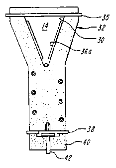
Referring to FIGURE 1 and 3, a channel
multiplier constructed in a form useful with the
present invention is shown at 10. It is comprised of
a monolithic electrically insulating, ceramic
material. It will be appreciated that the problems
of registration and seams in the channel passage, as
disclosed, for example in the above-discussed Patent
IO Nos. 3,244,922 and 4,095,133, are obviated by the
monolithic body.
In the embodiment shown in FIGURES 1 and 3,
the monolithic body 12 of the multiplier is
cylindrical in shape. As will be further noted. one
end of said body may be provided with a cone or
funnel shaped entryway or entry port 14 which evolves
to a hollow passageway or channel 16. The channel 16
preferably is three dimensional and may have one or
more turns therein which are continuous throughout
the body 12 of the multiplier 10 and e$its the
multiplier 10 at an ezit port at the opposite end 18
of the cylinder shaped body from the entryport 14.
It will also be appreciated that the passage of the
channel must be curved in applications where the
multiplier gain is greater than about 1 x 10⁶ to
avoid instability caused by °'ion feedback".
The surface 20 of the funnel shaped entryway
14 and the hollow passageway 16 is coated with a
semiconducting material having good secondary
emitting properties. Said coating is hereinafter
described as a dynode layer. As discussed further
below, in relation to FIGURE 7, the surface 20 may be
coated with a photoemission film 36a which acts as
the photoemission element of the invention.
WO 92/02946 ~ ~ ~ U ~ ~ C~ PCf/US91/0330?,..,
-10-
FIGURE 3 is a modified version of FIGURE 1,
wherein an input collar 44 is press fit onto the
ceramic body 12 and is used to make electrical
contact with entry port 14. An output flange 46 is
also pressed onto the ceramic body 12 and is used to
position and hold a signal anode 48 and also to make
electrical contact with exit port 18.
With reference to FIGURE 2 the embodiment
shown may be described as a free form channel
multiplier. In said embodiment, the multiplier 10,
comprises a tube-like curved body 22 having an
enlarged funnel-shaped head 24. A passageway 26 is
provided through the curved body 22 and communicates
with the funnel-shaped entrance way 28. It will be
appreciated that passageway 26 of FIGURE 2 differs
from passageway 16 of FIGURE 1 in that passageway 26
comprises a two-dimensional passage of less than one
turn. It is believed that the FIGURE 1 embodiment
may be preferable over the FIGURE 2 embodiment
depending on volume or packaging considerations. As
in the embodiment of FIGURES 1 and 3, the surface 30
of the passageway 26 and entrance way 28 are coated
with a dynode layer.
FIGURE 4 discloses a further embodiment of
the present invention wherein the channel multiplier
10 has the same internal configuration as that shown
in FIGURES 1 and 3, but has different external
configuration in that the body 32 is not in the form
of a cylinder. For reasons to be explained below
relating to the method of manufacturing the channel
multiplier of the present invention, almost any
desired shape may be employed for said multiplier.
Turning now to FIGURES 5 and 6, an
alternative embodiment of the present invention
~fl~~~.~a
W(? 92/02946 P('T/iJS91l03307
-11--
employing a plurality of hollow passageways or
channels therein is shown generally at 60. Channel
electron multiplier 60 is comprised of a unitary or
monolithic body 62 of ceramic material with a
multiplicity of hollow passages 64 interconnecting
front and back surfaces 66, 68 of body 62. It will
be appreciated that passages 64 may be straight,
curved in two dimensions, or curved in three
dimensions. Preferably, front and back surfaces 66,
68 are made conductive by metallizing them, while a
dynode layer is coated on the passageways.
FIGURE 7 is a sectional view, similar to
that shown in FIGURE 4, of an alternative embodiment
of the phototube of the present invention. In this
illustrated embodiment, a lead glass resistive dynode
material is disposed on the surface 20 of the funnel
shaped entryway 14 and into passageway 26. A
photoemission element 36a, in the form of
photoemission film, is then applied to surface 20 of
the funnel shaped entryway 14 overlying the dynode
material. In other embodiments, the photoemission
film is directly on surface 20, but not overlying the
dynode which eztends on the walls of the passageway
exterior to the funnel-shaped region. Other
locations for placement of the photoemission film may
be appropriate, depending upon the specific
configuration of the channel multiplier, and
consistent with the description herein. Elements
which correspond to elements in FIGURES 1-6 are
denoted with identical reference numerals.
FIGURE 8 is a sectional view, similar to
that shown in FIGURE 7, of an alternative embodiment
of the invention. In this illustrated embodiment,
the upper portion of the surface 20 of the entryway
WO 92/02946 ~ PCT/'U~911033Q?..
~~~~~~5 _12_
14 is coated with a metallized conductive coating 70,
such as nichrome. The coating 70 extends under the
faceplate, but is a transparent film in that region.
A film 70' may also coat the bottom of the multiplier
at B. The coating 70 may be used to inhibit charge
build-up on the surface 20, which distorts electron
flow. The conductive coating may also be used for
electrostatic field control. As shown in FIGURE 9,
the end of the multiplier denoted A may be grounded.
In the illustrated embodiment of FIGURE 8,
the transparent face plate 36 is coupled with the
body 62 by means of a conductive seal 72, such as an
indium alloy, or other maleable metal known generally
in the field. The seal element 72 is in physical and
electrical contact with the portions of conductive
coating 70 on entryway 14 and on faceplate 36. Also
shown in FIGURE 8 is an optional external pin 76,
which, as further shown in FIGURE 9, is more negative
than the end of the multiplier. In the illustrated
embodiment, a pin 76 extends into the passageway 14,
and includes a support 78 bearing a discrete
photocathode 78a which acts in a manner similar to
that of the photoemission film 36a described in
relation to FIGURE 7 above. It may also be used in
conjunction with such a photoemission film.
In practice, and as shown in the schematic
diagram of FIGURE 9, the device may include a power
supply 80 coupled between the cathode 78a at point C
and the anode at point D, with a resistive lead from
the positive end of the power supply 80 to the bottom
film 70' at point B. An output terminal 82 provides
an output signal.
The monolithic ceramic body of the
multiplier of the present invention may be fabricated
~,~3a~.~~
W~ 92/02946 PCT/US91/03307
-13-
from a variety of different materials such as
alumina, beryllia, mullite, steatite and the like.
The chosen material should be compatible with the
dynode layer material both chemically, mechanically
and thermally. It should have a high dielectric
strength and behave as an electrical insulator.
The dynode layer to be used in the present
invention may be one of several types. For example,
a first type of dynode layer consists of a glass of
the same generic type as used in the manufacture of
conventional channel multipliers. When properly
deposited on the inner passage walls, rendered
conductive and adequately terminated with conductive
material, it should function as a conventional
channel multiplier. Other materials which give
secondary electron emissive properties may also be
employed.
The ceramic bodies for the multiplier of the
present invention are fabricated using "ceramic°'
techniques.
In general, a preform in the configuration
of the desired passageway to be provided therein is
surrounded with a ceramic material such alumina and
pressed at high pressure.
After the body containing the preform has
been pressed, it is processed using standard ceramic
techniques, such as bisquing and sintering. The
preform will melt or burn-off during the high
temperature processing thereby leaving a passageway
of the same configuration as the preform.~
Following shaping, the body is sintered to
form a hard, dense body which contains a hollow
passage therein in the shape of the previously burnt
out preform. After cooling, the surface of the
WO 92/02946 ~ ~ ~ ~ ~ (~~ C~' PC,°T/U~91/0330'Z
--14 -.
hollow passage may be coated by known techniques with
a dynode material such as described earlier in this
application. In addition, the surface may be coated
by known techniques with a photoemission film, such
as also described earlier in this application.
Once the passageway has been coated with a
dynode material and, in one embodiment, the entryway
has been coated with a photoemission film, the
aperture end and the output end have been metallized,
the body may be fitted with various electrical and
support connections as shown in FIGURES 4 and 7, such
as an input collar or flange 35, a ceramic spacer
ring 34, transparent faceplate 36 having, in one
embodiment, a photoemission film 36a on its inner
surface (as shown in FIGURE 4), an output flange 38,
and ceramic seal 40 with a signal anode 42 attached
thereto. Alternatively, a discrete photoemission
element may be supported near the inner surface of
the faceplate. The faceplate 36 may be solid glass
or may be an array of optical fibers. The anode 42
may, for ezample, include a phosphor on a support
member, an array of charge-coupled diodes, or an
array of discrete charge collecting anodes, having a
metallic lead feeding through its support/seal 40.
These features are schematically represented by
member 42a in FIGURE 4a. In such configuration as
shown in FIGURE 4,' the device functions as a
phototube vacuum envelope electron multiplier. While
in the embodiment of FIGURE 4, the faceplate 36 is
coupled to the body 32 by discrete spacer ring 34 and
flange 35, the invention may also be configured with
the faceplate 36 coupled directly to the body 32. In
yet other forms of the invention, a high gain dynode
34a may be operatively positioned between the
WO 92/02946 ~ ~ ~ ~j ~ ~~ ~ PG'f/TJS91/03307
-15-
photoemission element of the photocathode and the
entrance port of the electron multiplier. In such
configurations, it is still considered that the
photoemission element is contiguous with the entrance
port of the electron multiplier.
With the configuration of FIGURE 4, with
either a monolithic body or multiple element body, a
separate glass or ceramic tube body, or other form of
vacuum envelope is not required. thus simplifying
IO fabrication of the phototube. Moreover, the
phototube of the invention is much. more rugged than
prior art devices with separate bodies. In such
prior art devices, the multipliers are mounted as
separate elements and are thus susceptible to damage
from vibration and shock.
With the phototube of the present invention
where the exterior surface of the monolithic ceramic
channel electron multiplier is at atmospheric
pressure and ambient temperature, heat generated on
the inner dynode surface is efficiently transferred
to this exterior surface where it can be efficiently
dissipated by convection cooling as well as radiation
and conduction cooling. This latter factor provides
a substantial operating advantage over the prior art
phototubes. The channel electron multiplier
phototube of the present invention provides signal
current levels greater than attained heretofore by
other types of channel electron multiplier (CEM)
phototubes. In fact,"the present invention provides
signal current levels approaching those of discrete
dynode phototubes, and, as a result, does not require
a separate resistor chain and multiple electrical
vacuum feedthru connections as do discrete dynode
multiplier phototubes.
WO 92/02946 ~ ~ ~ ~ ~ ~t ~ ~d.'T/US91/0330'~.
-16-
While preferred embodiments have been shown
and described, various modifications and
substitutions may be made thereto without departing
from the spirit and scope of the invention.
Accordingly, it is to be understood that the present
invention has been described by way of illustrations
and not limitation.
What is claimed is: