Note: Descriptions are shown in the official language in which they were submitted.
~asg~~~
BACKGROUND OF THE TNVENTION
The present invention relates to an optical soliton
pulse generator for high-speed fiber optic communication.
With the recent progress of optical amplification
techniques, the fiber optic communication technology is now
advancing toward ultra-long distance communication and it
is becoming a reality to implement fiber optic
communication across the Pacific Ocean without using any
regenerative repeaters. With conventional transmission
systems, however, an increase in the transmission rate
allows the influence of deterioration of the transmission
characteristic to grow which is based on the wavelength
dispersion characteristic and nonlinear optical effect of
the optical fiber, imposing limitations on the high-speed,
large-capacity transmission. Tn recent years an optical
soliton communication system has been in the limelight as a
system which surmounts the limitations on the speeding up
of transmission owing to the wavelength dispersion
characteristic and the nonlinear optical effect. The
optical soliton communication system is a system that makes
positive use of wavelength dispersion characteristic and
nonlinear optical effect of the optical fiber which are
contributing factors to the deterioration of the
transmission characteristics of prior art systems and that
transmits optical snort pulses intact while balancing the
broadening of pulses by the wavelength dispersion in the
optical fiber and the compression of pulses based on the
nonlinear optical effect. A time multiplex and a
wavelength multiplex system are also relatively easy to
_ 1 _
2Q88330
implement and are suitable for high-speed and large-
capacity transmission. Heretofore, a pulse light source
for the optical soliton communication has been implemented
by a semiconductor mode locked laser with an external
cavity or a gain switched semiconductor laser.
To realize the soliton communication utilizing the
optical fiber, an optical soliton pulse generating
technique is of importance. The conditions for the optical
pulse are that its temporal waveform is in the shape of a
squared hyperbolic secant (sech2t, where t is time) and
that its frequency spectrum does not excessively broaden
and is expressed by a Fourier transformation of the
temporal waveform (a Fourier transform limit). That is, it
is necessary that the product of the full width at half
maximum of the temporal waveform and the full width at half
maximum of the frequency spectrum be 0.315.
To suppress interference between adjacent optical
pulses which occurs on the optical fiber transmission line,
it is desirable that the pulse width be 20$ of or less than
the pulse interval.
Incidentally, in an experimental optical soliton
communication system at present, optical pulses are used
when the product of the full width at half maximum of the
temporal waveform and the full width at half maximum of the
frequency spectrum is within 0.441 or so.
A semiconductor mode locked laser with an external
cavity, which is a typical example of conventional optical
pulse generators, has a construction in which one end face
of the laser diode is given an anti-reflection coating, a
_ 2 _
2088330
reflector is disposed in front of the said one end face and
the other end face of the laser diode and the reflector
constitute an optical resonator. Since the semiconductor
laser is driven by a sinusoidaly modulated current signal
synchronized with the light round trip time of the optical
resonator, the modulation rate is fixed to the length of
the optical resonator and the product of the full width at
half maximum of the temporal waveform and the full width at
half maximum of the frequency spectrum exceeds 0.5.
Moreover, this method presents a problem in its long-term
stability as it employs the optical resonator which is
susceptible to changes in environmental conditions, for
example, a temperature change or mechanical vibration.
On the other hand, according to the gain switching
method which drives the semiconductor laser directly with
short current pulses, the modulation rate is not fixed in
principle, but in practice, it is hard to change the
modulation rate arbitrarily, because it is inevitable to
use a resonator type microwave circuit such as a comb
generator. With this method, the frequency spectrum
excessively broadens more than in the case of employing the
semiconductor mode locked laser, and the product of the
full width at half maximum of the temporal waveform and the
full width at half maximum of the frequency spectrum
becomes greater than 1. Consequently, no soliton optical
pulses can be obtained in this case; hence, it is necessary
to use a new technique for suppressing the excess spectral
brodening, such as a narrow-band optical filter.
In either case, since the oscillation wavelength of the
- 3 -
20~833U
laser undergoes substantial changes with its direct
modulation, the spectrum of pulses broadens excessively and
they cannot be used intact as optical pulses for the
soliton communication. Furthermore, it is difficult to
implement an optical soliton pulse generator which is
stable for a long period of time.
SUMMARY OF THE INVENTION
It is therefore an object of the present invention to
provide a short optical pulse generator for the soliton
communication which obviates the above-mentioned defects of
the prior art and which is variable in modulation rate and
hence is capable of generating optical pulses free from
excessive broadening of their spectra.
In an aspect, the present invention relates to an
optical pulse generator which is characterized by the
provision of: a semiconductor laser which oscillates
continuously at a single wavelength; a semiconductor
electro-absorption type optical modulator which performs
intensity modulation of the output light from the
semiconductor laser; a DC voltage source which applies to
the optical modulator a reverse DC voltage large enough to
extinguish the output light of the semiconductor laser; and
a sinusoidal voltage generator which applied a sinusoidal
voltage to the optical modulator.
In another aspect, the present invention relates to an
optical pulse generator which is characterized by the
provision of: a semiconductor laser which oscillates
continuously at a single wavelength; a first optical
modulator which performs intensity modulation of the output
- 4 -
2088330
light of the semiconductor laser; a second optical
modulator which performs intensity modulation of the output
light of the first optical modulator; a rectangular wave
generator which generates a rectangular pulse voltage for
driving the first and second optical modulators; and a
delay circuit which is provided between the second optical
modulator and the rectangular wave generator to delay the
rectangular pulse voltage of the rectangular voltage
generator for a predetermined period of time.
In still another aspect, the present invention relates
to an optical pulse generator which is characterized by the
provision of: a semiconductor laser which oscillates
continuously at a single wavelength; a first semiconductor
electro-absorption type optical modulator which performs
intensity modulation of the output light from the
semiconductor laser; a second semiconductor electro-
absorption type optical modulator which performs intensity
modulation of the output light from the first semiconductor
electro-absorption type optical modulator; a sinusoidal
voltage generator which generates a sinusoidal voltage for
driving the first and second semiconductor electro-
absorption type optical modulators; a DC voltage generator
which applies a reverse DC voltage to the first and second
semiconductor electro-absorption type optical modulators;
and a delay circuit which is provided between the second
semiconductor electro-absorption type optical modulator and
the sinusoidal voltage generator to delay the sinusoidal
voltage of the sinusoidal voltage generator for a
predetermined period of time.
- 5 -
208833
The first-mentioned optical pulse generator applies
semiconductor laser beams of a fixed intensity to the
semiconductor electro-absorption type optical modulator and
generates therefrom optical pulses through utilization of a
nonlinear characteristic of the optical modulation that its
optical output shows a monotonous decrease substantially
exponentially with an increase in the applied voltage.
This characteristic is inherent in the semiconductor
electro-absorption type optical modulator and is not found
in a dielectric optical modulator whose optical output
periodically varies with an increase in the applied
voltage. By applying to the semiconductor electro-
absorption type optical modulator a DC voltage biased to a
point where its optical output is sufficiently attenuated
and then by applying to the optical modulator a sinusoidal
voltage of an amplitude about twice larger that of the DC
voltage, the optical output pulse of the optical modulator
automatically becomes shorter than the sinusoidal voltage
by virtue of its nonlinear optical output characteristic
mentioned above and the semiconductor electro-absorption
type optical modulator can be operated so that it becomes
transparent for a short period of time. Thus, short
optical pulses can be generated. The temporal waveform of
the optical pulse obtainable with this method is
intermediate between squared hyperbolic secant and Gaussian
waveforms. By changing the bias voltage from a value at
which to obtain an extinction ratio of 10 dB to a value at
which to obtain an extinction ratio of 50 dB and by setting
the amplitude of each modulating voltage to twice that of
- 6 -
2088330
the bias voltage, the full width at half maximum of the
optical pulse obtainable in this instance changes from 25
to 10~ of the period of the sinusoidal voltage. Moreover,
since the semiconductor laser is caused to oscillate at a
fixed wavelength and since the short optical pulses are
produced by the semiconductor electro-absorption type
optical modulator without directly modulating the
semiconductor laser, the oscillation wavelength of the
semiconductor laser is free from variations which are
caused by the direct modulation of the laser, and hence it
is possible to suppress excessive broadening of the
spectrum, thus providing optical soliton pulses.
With the second-mentioned optical pulse generator,
semiconductor laser beams of a fixed intensity are applied
to the first optical modulator driven by a rectangular
voltage which provides a sufficient extinction ratio, and
the output light of the optical modulator is applied to the
second optical modulator driven by a rectangular voltage
which has a time difference between it and the above-
mentioned rectangular voltage. By this, the AND operation
of the driving waveform is performed in an optical domain,
thereby generating short optical pulses. The generation of
a very short voltage pulse waveform needs an ultrahigh-
speed electronic circuit, and hence is difficult. In
contrast thereto, the present invention permits the
production of short optical pulses by use of relatively
long rectangular voltage pulses. Since the optical pulse
width can be changed arbitrarily by setting the time
difference between the two rectangular voltage pulses, it
208833D
is possible to produce an optical pulse shorter than that
obtainable with the first-mentioned optical pulse
generator. The optical modulators may be either
semiconductor electro-absorption type optical modulators or
dielectric optical modulators.
With the third-mentioned optical pulse generator,
semiconductor laser beams of a fixed intensity are applied
to the first semiconductor electro-absorption type optical
modulator driven by a bias voltage and a sinusoidal voltage
of an amplitude more than twice that of the bias voltage
and the output light of the first optical modulator is
applied to the second semiconductor electro-absorption type
optical modulator driven by a bias voltage and a sinusoidal
voltage which has a time difference between it and the
above-mentioned sinusoidal voltage and has an amplitude
more than twice that of the bias voltage. By this, short
optical pulses are produced. By driving the semiconductor
electro-absorption type optical modulator with a sinusoidal
voltage of an amplitude more than twice that of the bias
voltage, an optical pulse waveform of very short rise and
fall times can be obtained owing to the nonlinearity of the
optical output characteristic. By clipping the optical
output pulse of the first semiconductor electro-absorption
type optical modulator by the second semiconductor electro-
absorption type optical modulator, it is possible to obtain
an optical pulse of very short rise and fall times. Since
the optical pulse width can be changed arbitrarily by
setting the time difference between the two sinusoidal
valtages, it is possible to produce optical pulses shorter
_ g _
2oss33o
than those obtainable with the first- and second-mentioned
optical generators.
BRIEF DESCRIPTION OF THE DRAWINGS
The present invention will be described in detail below
with reference to the accompanying drawings, in which:
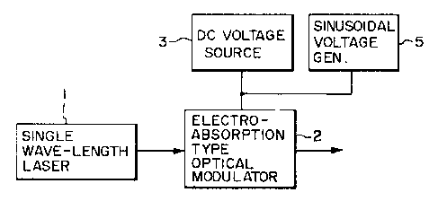
Fig. 1A is a block diagram illustrating in block form a
first embodiment of the optical pulse generator of the
present invention which uses a semiconductor electro-
absorption type optical modulator;
Fig. 1B illustrates a characteristic diagram explana-
tory of the principle of the generation of short optical
pulses by the semiconductor electro-absorption type optical
modulator in this embodiment;
Fig. 2A is a block diagram illustrating a second
embodiment of the optical pulse generator of the present
invention which employs two semiconductor electro-
absorption type optical modulators;
Fig. 2B illustrates time charts explanatory of the
principle of the generation of short optical pulses by the
semiconductor electro-absorption type optical modulators in
this embodiment;
Fig. 3A is a block diagram illustrating a third
embodiment of the optical pulse generator of the present
invention which employs two semiconductor electro-
absorption type optical modulators which are driven by a
sinusoidal voltage;
Fig. 3B illustrates waveform diagram explanatory of the
principle of the generation of short optical pulses by the
semiconductor electro-absorption type optical modulators in
- 9 -
2088330
this embodiment;
Fig. 9 is a sectional view showing the internal
construction of a fourth embodiment in which a
semiconductor laser and an electro-absorption type optical
modulator for generating pulses are integrated as a unitary
structure;
Fig. 5 is a sectional view showing the internal
construction of a fifth embodiment in which two electro-
absorption type optical modulators for generating pulses
are integrated as a unitary structure;
Fig. 6 is a sectional view showing the internal
construction of a sixth embodiment in which two electro-
absorption type optical modulators for generating pulses
and information signals, respectively, are integrated as a
unitary structure;
Fig. 7 is a sectional view showing the internal
construction of a seventh embodiment in which three
electro-absorption type optical modulators are integrated
as a unitary structure.
Fig. 8 is a sectional view showing the internal
construction of an eighth embodiment in which two electro-
absorption type optical modulators for generating pulses
and information signals, respectively, and a semiconductor
laser are integrated as a unitary structure.
Fig. 9 is a sectional view showing the internal
construction of a ninth embodiment in which three electro-
absorption type optical modulators and a semiconductor
laser are integrated as a unitary structure;
Fig. 10 is a block diagram illustrating an embodiment
- 10 -
2088330
of the present invention from which a modulated light
output is obtained;
Fig. 11 is a block diagram illustrating an embodiment
of the present invention from which a modulated light
output is obtained; and
Fig. 12 is a block diagram illustrating an embodiment
of the present invention from which a modulated light
output is obtained.
DETAILED DESCRIPTION OF PREFERED EMBODIMENTS
Embodiment 1]
A first embodiment is shown in Fig. 1A of a block
diagram of the optical pulse generator, Fig. 1B a graph for
explaining the principle of generating short optical pulses
by a semiconductor electro-absorption type optical
modulator.
A description will be given first of the principle of
operation of the invention. In Fig. 1A, fixed output light
of a 1.55 ,um wavelength, which is emitted from an InGaAsP
~l/4 shift distributed feedback (DFB) single-wavelength
laser 1, is applied to an InGaAsP electro-absorption type
optical modulator 2, A forbidden band wavelength of the
InGaAsP modulation waveguide layer of the optical modulator
1 is set between 1.44 and 1.5 ,um. When supplied with no
voltage, the optical modulator 1 is substantially
transparent, but it absorbs light and does not transmit it
therethrough as a reverse voltage applied thereto
increases. Fig. 1B shows, on a log scale, the transmission
characteristic (the extinction ratio) of the electro-
absorption type optical modulator with respect to the
- 11 -
~0~~330
reverse voltage applied thereto. The extinction ratio
scaled in dB of the electro-absorption type optical
modulator is substantially in proportion to the reverse
voltage applied thereto. That is, the optical output is
nonlinear with respect to the voltage. A bias voltage 4 is
applied from a DC voltage source 3 to a point where
substantially no light passes through the optical
modulator, as shown in Fig. 1B. Then, the amplitude of a
modulation voltage 6 which is the output of a sinusoidal
voltage generator 5 is set to around twice larger than that
of the bias voltage 4 and the modulation voltage is applied
to the optical modulator, by which short optical pulses 7
can be obtained.
To confirm the above-noted effect, the inventors of
this application tested the operation of this embodiment
which employed an InGaAsP ~/4 shift DFB laser oscillating
at a single wavelength of 1.55 ,um and an electro-absorption
type optical modulator having an InGaAsP modulation
waveguide layer of a 1.45 ,um forbidden band wavelength. In
this tests, when the bias voltage was -3 V, the optical
modulator output was reduced down to 1/100 (an extinction
ratio of 20 dB) that in the case of the bias voltage being
zero. Furthermore, by applying a 5-GHz sinusoidal
modulation voltage of a 6 V amplitude to the optical
modulator, an ultrashort optical pulse was obtained which
had a full width at half maximum of 40 picoseconds. When
the bias voltage was changed from -2 V to -6 V and the
amplitude of the bias voltage was set twice the bias
voltage, the full width at half maximum of the optical
- 12 -
~08833~
pulse changed from 49 picoseconds to 22 picoseconds. Since
the period of the sinusoidal voltage was 200 picoseconds,
pulse widths in the range of 24.5 to 11$ of the period were
obtained.
The present invention does not utilize such an optical
resonator as in the case of the prior art example, and
hence permits arbitrary setting of the modulation rate. In
the tests of this embodiment, the frequency of the
sinusoidal voltage was set to 15 and 20 GHz. When the bias
voltage was -2 V and the amplitude of the sinusoidal
voltage was 7.2 V, short optical pulses whose full widths
at half maximum were 14 and 11 picoseconds were obtained
when the frequency of the sinusoidal voltage was 15 and 20
GHz, respectively. Since the 3 dB bandwidth of the
frequency characteristic of the optical modulator used was
7 GHz, the modulation efficiency at 15 and 20 GHz was 4 and
6 dB lower than that in the case of DC voltage. It was
found, however, that the modulation rate could freely be
selected, in principle, by increasing the modulating
voltage in a manner to make up for such deterioration of
the modulation efficiency.
Next, measurements of light spectrums were made. The
full widths at half maximum of the spectral envelop of
temporal waveforms which has repetition frequencies of 5
and 15 GHz and full widths at half maximum of 22 and 14
picoseconds were 14 and 23 GHz, respectively. The product
of the full width at half maximum of the temporal waveform
and the full width at half maximum of the spectral envelop
was 0.32 in either case. This value is very close to the
- 13 -
208833
product, 0.315, of the full width at half maximum of the
temporal waveform and the full width at half maximum of the
spectral envelop of the squared hyperbolic secant waveform
which is the requirement for the soliton pulse. The
optical pulse obtainable with the present invention
substantially satisfies the soliton requirement and has a
pulse width to be 20~ of or smaller than the pulse
interval, and hence it can be applied to the soliton fiber
optic communication system. Then, a train of short pulses
having a 60 psec full width at half maximum and a 2.48 GHz
repetition frequency, produced by the pulse generator of
this embodiment, was transmitted over an optical fiber
10,000 km long and pulse waveforms were observed. No
remarkable deterioration was observed in the pulse
waveforms even after the pulses were transmitted 10,000 km.
This proves that the optical pulse generator of this
embodiment can be used as a soliton light source for a long
distance optical soliton communication.
Incidentally, the light output characteristic in
logarithmic scale or the extinction ratio scaled in dB of
the electro-absorption type optical modulator need not
always be linear to the applied voltage. In the case where
the extinction ratio linearly increases in a low voltage
region and the rate of its increase in a high voltage
region slightly lowers, the resulting temporal waveform
becomes closer to the squared hyperbolic secant waveform.
This phenomenon was observed when the optical axes of an
optical fiber and optical modulators disposed at its input
and output ends with lenses or the like interposed there-
- 14 -
208833t~
between were slightly out of alignment.
In the case where the extinction ratio scaled in dB
linearly increases in the low voltage region and the rate
of its increase slightly increases in the high voltage
region, the resulting temporal waveform becomes very close
to the Gaussian waveform. In either case, such a waveform
variation is permissible in the case of the soliton light
source. Moreover, when the wavelength of light incident to
the optical modulator was changed from 1.52 to 1.57 ,um in
this embodiment, short optical pulses of about the same
waveform could be obtained.
The pulse generator of this embodiment permits easy
adjustment of the pulse width, and hence can be used not
only to generate optical soliton pulses but also as an
optical pulse generator which utilizes ordinary return-to-
zero codes. The optical pulse generator of this embodiment
does not employ an optical resonator, and hence is
advantageous in that it is insusceptible to changes in
temperature and other environmental conditions, that the
modulation rate is variable, and that short optical pulses
for the soliton communication, which is free from excessive
spectral line broadening, can easily be generated by use of
only the sinusoidal voltage without the necessity of using
a special microwave voltage generator.
It is postulated that a practical application of this
embodiment will involve the use of a second optical
madulator, as shown in Fig. 10, for generating an informa-
tion signal which is added to the output light of the
semiconductor electro-absorption type optical modulator 2.
- 15 -
2088330
[Embodiment 2]
Fig. 2A is a block diagram illustrating a second
embodiment of the present invention and Fig. 2B is a
diagram for explaining the principle of generating a short
pulse. The feature of this embodiment resides in the
generation of short pulses by driving two electro-
absorption type optical modulators with modulating voltages
of different durations unlike in Embodiment 1.
Fixed output light of a 1.55 ,um wavelength, emitted
from an InGaAsP ~/4 shift DFB single-wavelength laser 1, is
applied to a first InGaAsP electro-absorption type optical
modulator 2. The first optical modulator 2 is driven by a
rectangular voltage (pulse width T1) of a 3 V amplitude (0
to -3V) and a 5 GHz repetition frequency, which is one of
two outputs branched from the output of a rectangular wave
generator 9. Since the rectangular voltage generator 9 can
generate a pulse voltage whose rise time and fall time are
around 10 picoseconds unlike the sinusoidal voltage
generator, optical output pulses from the first InGaAsP
electro-absorption type optical modulator 2 are rectangular
optical pulses having an extinction ratio of 20 dB or more.
These optical pulses are fed to a second InGaAsP electro-
absorption type optical modulator 8. The other branched
output voltage from the rectangular voltage generator 9 is
applied to a delay circuit 10 (of a delay time T) which is
formed by a coaxial line or the like, and the delayed
rectangular voltage from the delay circuit 10 is applied to
the second optical modulator 8 to drive it. With such a
construction, an AND operation of the modulating voltage is
- 16 -
~08833(~
possible in the optical domain and the light incident to
the optical modulator 2 provides, at the output of the
optical modulator 8, a short optical pulse of a pulse width
corresponding to the time difference between the pulse
width T1 and the delay time T. When the delay time is set
to 180 picoseconds, the pulse width, T1 - T, of the optical
output pulse is 20 picoseconds or below.
While it is difficult to generate a modulating voltage
of a very short pulse width in the stage of an electrical
signal, this embodiment permits the production of a short
optical pulse of an arbitrary pulse width through
utilization of the time difference between two relatively
long modulating voltage pulses. Hence, the pulse generator
of this embodiment can be used not only to generate optical
soliton pulses but also as an optical pulse generator which
utilizes ordinary return-to-zero codes.
According to inventors' performance tests of this
embodiment employing the above-mentioned InGaAsP electro-
absorption type optical modulators, optical waveforms of 20
to 30 psec rise and fall times were obtained as outputs
from the optical modulator which was driven by the
rectangular voltage. It is possible, therefore, to produce
ultrashort pulses having a pulse Width of 20 picoseconds or
below by the use of two modulators.
Incidentally, since the optical modulators used in this
embodiment can be applied to all intensity modulators,
their constructions and materials do not matter. Hence,
they are not limited specifically to the semiconductor
optical modulators but may also be dielectric optical
- 17 -
2088330
modulators using LiNb03 or the like.
It is postulated that a practical application of this
embodiment will involve the use of a third optical
modulator, as shown in Fig. 11, for producting an informa-
tion signal which is added to the output light from the
semiconductor electro-absorption type optical modulator 8.
[Embodiment 3]
Fig. 3A is a block diagram illustrating a third
embodiment of the present invention and Fig. 3B is a
diagram for explaining the principle of generating short
pulses. The feature of this embodiment resides in the
generation of short pulses by driving two electro-
absorption type optical modulators with a sinusoidal
modulating voltage and a bias voltage which have a time
difference therebetween unlike Embodiment 2.
Fixed output light of a 1.55 ,um wavelength, emitted
from the InGaAsP X1/4 shift DFB single-wavelength laser 1,
is applied to the first InGaAsP electro-absorption type
optical modulator 2. A reverse bias voltage -3 V is
applied to the first optical modulator 2 from the DC
voltage source 3. The output from the sinusoidal generator
5 is branched into two, and a sinusoidal voltage of a 5 GHz
frequency, which is one of the two outputs, is applied to
the first optical modulator 2 after the amplitude of the
sinusoidal voltage is increased to 9 V which is more than
twice the bias voltage. When the semiconductor electro-
absorption optical modulator is driven by such a sinusoidal
voltage of an amplitude more than twice the bias voltage,
the optical output characteristic of the optical modulator
- 18 -
208833U
nonlinearly decreases with respect to the reverse voltage
and undergoes substantially no change with respect to a
forward voltage as depicted in Fig. 1B. This provides a
rectangular optical pulse which is very short in its rise
and fall times, and hence the optical output pulse from the
first InGaAsP electro-absorption type optical modulator is
a rectangular optical pulse which has an extinction ratio
of more than 20 dB and is extremely short in its rise and
fall times. Such an optical pulse is applied to the second
InGaAsP electro-absorption type optical modulator 8. The
bias voltage -3 V from the DC voltage source 13 is applied
to the second optical modulator 8, to which is further
applied the other output sinusoidal voltage branched from
the output voltage of the sinusoidal voltage generator 9
via the delay circuit 10 (of the delay time T) formed by a
coaxial cable or the like. With such a construction, it is
possible to perform the AND operation of the rectangular
optical pulse although the optical modulators are driven by
the sinusoidal voltage, and the light incident to the
optical modulator 2 is derived from the optical modulator 8
as a short optical pulse of a pulse width corresponding to
the time difference between the pulse width T1 and the
delay time T. When the delay time T is set to 190
picoseconds, the pulse width, T1 - T, of the optical output
pulse becomes shorter than 10 picoseconds.
Incidentally, it is postulated that a practical
application of this embodiment will involve the use of a
third optical modulator, as shown in Fig. 12, for producing
an information signal which is added to the output light of
- 19 -
2088330
the semiconductor electro-absorption type optical modulator
8.
[Embodiment 4]
Fig. 4 is a sectional view illustrating, as a part of a
fourth embodiment of the present invention, a device or
element in which the afore-mentioned semiconductor laser
and the electro-absorption type optical modulator for
generating short pulses are integrated. The InGaAsP .1/4
shift DFB single-wavelength laser 1 and the InGaAsP
electro-absorption type optical modulator 2 used in the
optical pulse generator of Embodiment 1 are integrated on
an InP semiconductor substrate 11. The both elements are
electrically isolated by a semi-insulating InP layer 12.
The inventors made an integrated device in which the
laser portion was 300 ,um long, the semi-insulating InP
layer 12 was 50 ,um long and the modulator portion was 290
,um long. Either end face of the integrated device is
coated with an anti-reflection film to suppress variations
in the oscillation wavelength which is caused by the
reflection of light from the optical modulator to the
laser. The electric isolation resistance between the laser
and the optical modulator is 1 megohm and suppresses the
electric interference between them. The isolation
resistance of 1 megohm is enough large to suppress
wavelength variations of the laser and to obtain the
transform-limited short pulses. The forbidden band energy
of an InGaAsP modulating waveguide layer is 1.45,um. When a
180 mA direct current was applied to the laser portion, it
oscillated at a single wavelength of 1.55 ,um, and when a
- 20 -
2088330
-2 V bias voltage was applied to the modulator portion, an
extinction ratio of 25 dB was obtained. Moreover, when a
sinusoidal voltage of a 5 GHz frequency and a 4 V amplitude
was provided to the optical modulator portion, an optical
pulse was obtained the full width at half maximum of which
Was 33 picoseconds. It was ascertained that the product of
full width at half maximum of the temporal waveform and the
full width of half maximum of the spectral envelop was
0.31, which is very close to the value of 0.315 for
transform-limited sech2 pulse and sufficient for the
soliton light source.
While this embodiment has been described to employ an
InGaAsP ~/4 shift DFB laser as the single-wavelength laser,
it may also be replaced by other single-wavelength lasers
of any construction, such as a distributed Bragg-reflector
laser and an ordinary DFB laser using a homogeneous or
uniform diffraction grating, and a variable wavelength
laser is also applicable. Moreover, this embodiment is not
limited specifically to semiconductor materials of any
ZO particular series, and a quantum well structure may also be
applied to the active layer of the laser and the modulating
waveguide layer.
The feature of the optical pulse generator according to
this embodiment lies in that since the laser and the
modulator are formed as a unitary structure, the optical
coupling loss between them is substantially reduced in the
one-chip semiconductor device and the DC voltage and the
sinusoidal voltage are small because of high modulation
efficiency.
- 21 -
2088330
[Embodiment 5]
Fig. 5 is a sectional view illustrating, as a part of a
fifth embodiment of the invention, a device in which two
electro-absorption type optical modulators for generating
short pulses are integrated. In this embodiment, the two
InGaAsP electro-absorption type optical modulators 2 and 8
used in Embodiments 2 and 3 are integrated on the InP
semiconductor substrate 11. The both elements are
electrically isolated from each other. The integrated
elements are formed by InGaAsP modulating layers of the
same composition, and hence are easy of crystal growth and
cause no optical coupling loss between them. The electro-
isolation resistance between the both elements can be made
more than 1 megohm by the adoption of the semi-insulating
InP layer 12.
An integrated optical modulator for optical pulse
generator of this embodiment comprises a semiconductor
substrate, a first optical modulator for modulating an
intensity of an input light, and a second optical modulator
for modulating the intensity of the output light from the
first optical modulator, and moreover, the first optical
modulator and the second optical modulator are integrated
as a unitary structure on the semiconductor substrate.
The feature of this embodiment resides in that no
optical coupling loss is caused between the two optical
modulators because they are formed as a unitary structure.
[Embodiment 6]
Fig. 6 is a sectional view illustrating, as a part of a
sixth embodiment of the present invention, a device in
- 22 -
2088330
which an electro-absorption type optical modulator for
generating short pulses and an electro-absorption type
optical modulator for generating information signals are
integrated. In this embodiment, the InGaAsP electro-
absorption type optical modulator 2 for generating short
pulses, used in Embodiment 1, and an InGaAsP electro-
absorption type optical modulator 13 for producing
information signals are integrated on the InP semiconductor
substrate 11, and the both elements are electrically
isolated from each other by the semi-insulating InP layer
12.
An integrated optical modulator for optical pulse
generator of this embodiment comprises a semiconductor
substrate, a semiconductor electro-absorption type optical
modulator for modulating an intensity of an input light,
and an optical modulator for modulating the intensity of
the output light from the first optical modulator, and
moreover, the semiconductor electro-absorption type optical
modulator and the optical modulator are integrated as a
unitary structure on the semiconductor substrate.
The feature of this embodiment resides in the
additional provision of a signal generating modulator to
Embodiment 1 without causing an increase in the optical
loss.
[Embodiment 7]
Fig. 7 is a sectional view illustrating, as a part of a
seventh embodiment of the present invention, a device in
which two electro-absorption type optical modulators for
generating short pulses and an electro-absorption type
- 23 -
2088330
optical modulator for generating information signals are
integrated. In this embodiment, the two InGaAsP electro-
absorption type optical modulators 2 and 8 in Embodiment 5
and an InGaAsP electro-absorption type optical modulator 13
for generating information signals are integrated together
on the InP semiconductor substrate 11, and the three
elements are electrically isolated by the semi-insulating
InP layer 12.
An integrated optical modulator for optical pulse
generator of this embodiment comprises a semiconductor
substrate, a first optical modulator for modulating an
intensity of an input light, a second optical modulator for
modulating the intensity of the output light from the first
optical modulator, and a third optical modulator for
modulating the intensity of the output light from the
second optical modulator, and moreover, the first optical
modulator, the second optical modulator and the third
optical modulator are integrated as a unitary structure on
the semiconductor substrate.
the feature of this embodiment is a fact that the
signal generating modulator can be newly added to
Embodiment 5 without causing an increase in optical loss,
because the three modulators are formed as a unitary
structure.
[Embodiment 8]
Fig. 8 is a sectional view illustrating, as a part of
an eighth embodiment of the present invention, a device in
which two electro-absorption type optical modulators and a
semiconductor laser are integrated. In this embodiment,
- 24 -
2088330
the two InGaAsP electro-absorption type optical modulators
2 and 8 in Embodiment 5 or the InGaAsP electro-absorption
type optical modulator 2 for generating short pulses and
the InGaAsP electro-absorption type optical modulator 13
for generating information signal in Embodiment 6 are
integrated on the InP semiconductor substrate 11, together
with the InGaAsP ~/4 shift DFB single-wavelength laser 1.
The three elements are electrically isolated by the semi-
insulating InP layer 12.
An integrated optical pulse generator for optical
soliton communications of this embodiment comprises a
semiconductor substrate, a semiconductor laser for
continuously oscillating an output light at a single
wavelength, a first optical modulator for modulating an
intensity of an input light, and a second optical modulator
for modulating the intensity of the output light from the
first optical modulator, and moreover, the semiconductor
laser, the first optical modulator and the second optical
modulator are integrated as a unitary structure on the
semiconductor substrate.
[Embodiment 9]
Fig. 9 is a sectional view illustrating, as a part of a
ninth embodiment of the present invention, a device in
which two electro-absorption type optical modulators for
generating short pulses, another electro-absorption type
optical modulator for generating information signals and a
semiconductor laser are integrated. In this embodiment,
the two InGaAsP electro-absorption type optical modulators
2 and 8 for generating short pulses and the InGaAsP
- 25 -
2088330
electro-absorption type optical modulator 13 for generating
information signals in Embodiment 7 and the InGaAsP ~/4
shift DFB single-wavelength laser 1 are integrated as a
unitary structure on the InP semiconductor substrate 11.
The four elements are electrically isolated by the semi-
insulating InP layer 12.
An integrated optical pulse generator for optical
soliton communications of this embodiment comprises a
semiconductor substrate. a semiconductor laser for
continuously oscillating an output light at a single
wavelength, a first optical modulator for modulating an
intensity of an input light, a second optical modulator for
modulating the intensity of the output light from the first
optical modulator, and a third optical modulator for
modulating the intensity of the output light from the
second optical modulator, and moreover, the semiconductor
laser, the first optical modulator, the second optical
modulator, and the third optical modulator are integrated
as a unitary structure on the semiconductor substrate.
With the construction of this embodiment, it is
possible to obtain a short pulse generator of extremely low
loss since the laser, the two short pulse generating
modulators and the information signal generating modulator
are formed as a unitary structure.
While in the above the present invention has been
described to employ InGaAsP electro-absorption type optical
modulators, it is also possible to use absorption type
optical modulators of a quantum well structure wherein the
quantum well layer is formed by an InGaAsP or InGaAs layer
- 26 -
2oss33o
and a quantum barrier layer is formed by an InP or InGaAsP
layer which has a forbidden band energy larger than that of
the quantum well layer. Furthermore, absorption type
optical modulators of InGaAlAs/InAlAs and InGaAs/InAlAs
quantum well structures can also be used in the present
invention.
The two optical modulators for generating short optical
pulses and the modulator for generating information signals
can be formed by any kinds of intensity modulator
irrespective of their constructions and materials. Hence,
the optical modulators for use in the present invention are
not limited specifically to semiconductor optical
modulators but may also be dielectric optical modulators
using LiNb03 or the like.
As regards the integrated optical pulse generator, two
or more arbitrary combinations of the laser and the
modulators are possible and the above-mentioned quantum
well structure can be used.
Although in the above the pulse generators of the
present invention have been described to be used for the
soliton optical communication, they can also be used as
optical pulse generators utilizing ordinary return-tc-zero
codes.
Moreover, ultrashort optical pulses having a pulse
width of 1 picosecond or less could be obtained by
utilizing the nonlinearity of an optical fiber or pulse
compression effect by a saturable absorber after the
generation of optical pulses by the present invention.
The present invention has such a construction as
- 27 -
208833t~
described above, and hence produces the following effects.
The optical pulse generator according to the first
aspect of the invention achieves the variable modulation
rate and suppresses the excessive spectral line broadening,
both impossible with the prior art, by a simple method
which employs a semiconductor laser, an electro-absorption
type optical modulator, a DC voltage source and a
sinusoidal voltage generator, and the pulse generator is
capable of generating ultrashort optical pulses free from
the excessive spectral line broadening, and hence is very
promising as an optical pulse generator for the soliton
communication which is stable and reliable for a long
period of time.
The optical pulse generator according to the second
aspect of the invention is able to produce short optical
pulses of arbitrary pulse widths by changing the delay time
of a rectangular voltage signal to be applied to one of two
optical modulators, and hence is capable not only of
achieving the variable modulation rate and suppressing the
excessive spectral line broadening but also of easily
generating short optical pulses of a pulse width smaller
than 1/10 the pulse-repetition period. Hence, this pulse
generator is also very promising as an optical pulse
generator for the soliton communication.
The optical pulse generator according to the third
aspect of the invention is capable not only of achieving
the variable modulation rate and suppressing the excessive
spectral line broadening but also of easily generating
short optical pulses of a pulse width smaller than 1/10 the
- 28 -
2os..s3~~
pulse-repetition period, without the need of using any
special high-speed electronic circuit, by changing the
delay time of a sinusoidal voltage signal to be applied to
one of two electro-absorption type optical modulators.
Hence, this pulse generator is also very promising as an
optical pulse generator for the soliton communication.
The inventors think that the first-mentioned optical
pulse generator is most promising from the viewpoints of
easiness of handling of the device and its single-frequency
operation and that the third-mentioned optical pulse
generator is suitable for generating short optical pulses
of smaller pulse widths.
20
- 29 -