Note: Descriptions are shown in the official language in which they were submitted.
r- f~ ~ !~ ~,
~, ~ . .r
2~88~4'~
PATENT
450100-2714
1 TITLE OF THE INVENTION
2 METHOD AND APPARATUS FOR ENCODING A DIGITAL IMAGE SIGNAL
3 BACKGROUND OF THE INVENTION
4 The present invention relates to encoding of a digital
image signal,, and more particularly relates to framing of the
6 encoded digital image signal so as to be more readily
7 reproducible.
8 Digital video tape recorders (VTRs) employ a rotary
9 head or heads for recording a digital video signal in slant
tracks on a magnetic tape. Other existing digital video
11 recorders record in substantially circular tracks on a disk-
12 shaped recording medium. In either case, each frame or field of
13 the digital video signal is recorded in a plurality of tracks,
14 and each track 'typically contains blocks of highly efficiently
coded data which represent the image data.
16 A digital image signal, also referred to as a digital
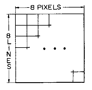
17 video signal, is typically encoded for recording by first
18 converting the signal into blocks of image data. Fig. 1A shows a
19 typical image data block comprised of the data for 8 pixels in 8
lines, and referred to as an (8 x 8) block. Each block is
21 orthogonally transformed using, for example, a discrete cosine
22 transform (DCT) to pxoduce a transformed image data block or set
23 of transform coefficients representing the image data block and
24 consisting of one DC coefficient and many AC coefficients.
BP13:2714.APP 1
2~~~~4~
4
PATENT
450100-2714
1 The transformed image data block is scanned in a zigzag
2 manner, as shown in Fig. 1B, to produce a sequence of
3 coefficients which are in a roughly ascending frequency order and
4 which are quantized. The quantized AC coefficients, representing
AC components of the image data block, are coded using a variable
6 length code, such as, run length encoding followed by Huffman
7 coding. The quantized DC coefficient data has affixed length,
8 such as nine bits. A framing circuit forms the encoded data of
9 variable length per image data block into sync blocks of fixed
length, and which each include a synchronization (sync) signal
11 and an identification (ID) signal, so as to be more readily
12 reproducible by a reproducing system.
13 When component signals (Y, U and V) are encoded via
14 DCT, a unit referred to as a macro block is used. In the 4:1:1
system for 525/60 video signals, a macro block is comprised of
16 four transformed image data blocks representing luminance
17 information (YYYY), each of size 4 x l, and which are arranged in
18 a horizontal row, and two transformed image data blocks
1~ representing color difference information (U and V) and which are
at the same spatial position, as shown in Fig. 2A. In the 4:2:0
21 system, a macro block is comprised of four transformed image data
22 blocks representing luminance information (YYYY), each of size 2
23 x 2, and which are arranged in a square, and two transformed
24 image data blocks representing color difference information (U
and V) and which are at the.same spatial position, as shown in
BP13:271G.APP 2
PATENT
450100-2714
1 Fig. 2B. In other words, a macro block consists of six
2 transformed image data or DCT blocks.
3 A temporal sequence of these component DCT blocks is
4 shown in Fig. 2C, while Fig. 2D represents the temporal sequence
in a more convenient form, with two macro blocks outlined. Only
6 data which is from tha same macro block can properly be combined
7 during reproduction by the digital VTR to produce a reproduced
8 image. Therefore, even if luminance data Y and color difference
9 data U and V from different~macro blocks are reproduced, as shown
by the dashed line in Fig. 2D, a proper image cannot be produced.
11 In order to ensure that the variable length encoded
12 data fits into the fixed length sync blocks, the amount of
13 encoded data in a particular interval is restricted to be within
I 14 a target value during the encoding or buffering process. The
amount of encoded data which is constrained to be within this
16 target value is referred to as an encoding set or a buffering
17 unit. For example, the amount of encoded data may be restricted
18 by altering the quantization step size, possibly in accordance
19 with a quantizing number generated by a control circuit; and the
quantization step size or quantizing number is inserted into the
21 sync block with the. encoded data. Fig. 3A shows a sync block
22 having a byte width and including a sync signal, an ID signal, a
23 data area and a parity code area: The first item in the data area
24 is the quantizing number QNO. '
Then an error occurs in the variable length encoded
BP13:2714.APP 3
PATEidT
450100-2714
1 data or code signals, it becomes difficult to distinguish
2 subsequent code signals, that is, the error is propagated so that
3 the data subsequent to the error cannot be decoded. The sync
4 block format shown in Fig. 3A has been said to be resistant to
propagation errors due to the arrangement of encoded data within
6 the data area. In particular, the data area shown in Fig. 3A has
7 fixed length areas which contain encoded data for each of the
8 component DCT blocks.
9 The encoded data or code signals DC representing the DC
components are of fixed length (nine bits), whereas the encoded
11 data or. code signals AC representing the AC components are of
12 variable length. Thus, the amounts of data in the. transformed
13 image data blocks are not necessarily equal. As shown in Fig. 3B,
14 the AC component data for a particular transformed block are
inserted into a particular fixed length area immediately
16 following the DC component data for that particular transformed
17 block.
18 If the DC and AC component data do not fill the
19 particular length area, then the area has unused capacity,
fixed
shown by shadingin the areas YO, Y1, Y3 and C0. An end
of block
21 (EOB) code signalis inserted at the'end of 'the component
data
22 for particulartransformed image data block, as shown
a in Fig.
23 3B.
24 If some of the AC component data of the particular
transformed block does not fit into the corresponding particular
BP13:2714.APP 4
2~~~~~~
PATENT
450100-2714
1 fixed length area, that is, exceeds its capacity or overflows,
2 fox example, which is the case for areas Y2 and Yn in Fig. 3B,
3 then these overflow data are sequentially inserted into unused
4 portions of other fixed length areas starting from the beginning
of the sync block.
6 Due to the zigzag scanning of the AC components, the
7 overflow AC component data corresponds to relatively high
8 frequencies. For convenience, high frequency code signals are
9 referred to as AC-H, and the blank or unused portions of fixed
, length areas, shown by shading in Fig. 3B, are referred to as AC-
11 H areas, more particularly, as variable AC-H, areas since their
12 lengths differs depending on the image. Similarly, encoded data 1
13 representing relatively low frequencies are referred to as AC-L,
14 and the areas in which they are located are referred to as AC-L
areas.
16 In the example shown in Fig. 3B, AC-Hs which overflowed
17 from the area Y2 are placed in the area Y0. Of'course, depending
18 on the image, the area YO may be filled, and in such case the
19 overflow from area Y2 would be placed in the first area having an
unused portion, that is, a first variable AC-H area. In other
21 situations, the transformed image data may not overflow from the
22 area Y2, but may overflow from other areas; this overflow data
23 would similarly be placed in the first available variable AC-H
24 area. In short, there is no predetermined relationship between
the AC-H components for each of the transformed image data blocks
BP13:2714.APP 5
2~8~~~~
PATENT
450100-2714
1 and the variable AC-H areas into which these AC-H components are
2 placed.
3 The sync block arrangement shown in Fig. 3B prevents an
4 error from being propagated in the DC and AC-L areas. For
example, an error in a DC area renders the remaining bits of that
6 DC area useless. However, since the starting position of the AC-L
7 area is known, namely, the tenth bit of the fixed length area,
8 the error in the DC area does not propagate.
9 Unfortunately, the AC-H areas lack resistance to errors
propagated from the AC-L areas. This is a problem, because, the
11 high frequency AC components are not reproduced, that is, 'if only
12 the DC and low frequency AC components of a transformed block are
13 reproduced, the displayed image exhibits a mosaic-like
14 distortion.
For example, when an error occurs in the variable
16 length encoded data CC1 shown in the AC-L area of area YO of Fig.
17 3B, the EOB code in that AC-L area cannot be detected, and so the
18 position of the variable AC-H area in area YO cannot be
19 determined. In fact, all of the variable AC-H areas in the sync
block which are subsequent to the variable AC-H area having an
21 error are also rendered useless by error propagation, as shown in
22 Figs. 3C and 3D.
23 Since there is no predetermined relationship between
24 the AC-H components and AC-H areas, in a variable speed
reproducing mode in which data is reproduced at a higher speed
BP13:2714.APP 6
2f~~8~~"~
PATEriT
450100-2714
1 than in a recording mode, code signals of the variable AC-H areas
2 cannot be used, and therefore the resultant reproduced image
3 exhibits mosaic-like distortion. This is because each sync block
4 of reproduced data is treated as valid data, and successive sync
blocks cannot always be obtained as valid data. In other words,
6 high speed reproduction of sync blocks having the structure shown
7 in Fig. 3A results in reproduction of usable DC and low frequency
8 AC components, but fails to effectively reproduce high frequency
9 AC components.
Furthermore, in the sync block shown in Fig. 3A, there
11 is no predetermined relationship between a macro block and a sync
12 block. Thus, even if all code signals of one sync block are
13 properly reproduced, it may still be impossible to properly
14 reproduce a macro block. This is a problem when reproducing at a
variable speed.
16 DHJECTS AND SUMMARY OF 'fHE INVENI'I~N
17 An object of the present invention is to provide a
18 method and apparatus for encoding a digital image signal which
19 avoid the aforementioned disadvantages of the prior art.
More specifically, it is an object of the present
21 invention to encode a digital image signal so that a macro block
22 of component data may be reproduced at a variable speed.
23 Another object of~the present invention is to encode a
24 digital image signal so as to minimize the occurrence of
propagation errors.
BP13:2714.APP 7
PATENT
450100-2714-
1 A further object of the present invention is to encode
2 a digital image signal to promote the reproducibility of high
3 frequency AC components, as well as DC components arid low
4 frequency AC components, and to thereby minimize mosaic-like
distortion in a reproduced image.
6 A still further object of the present invention is to
7 encode a digital image signal so that macro blocks representing
8 central portions of an image are less susceptible to errors than
9 macro blocks representing less centrally located portions of the
image.
11 According to an aspect of the present invention, a
12 ° digital image signal is encoded by orthogonally transforming the
13 same into transformed macro blocks containing DC and low
14 frequency AC components of the digital image signal, encoding an
encoding set comprised of a predetermined number of the
16 transformed macro blocks using a variable length code into an
17 amount of encoded data in accordance with a target amount, and
18 forming the encoded data corresponding to an approximately
19 integer number of transformed macro blocks into a sync block
having a fixed length and also having DC component areas and low
21 frequency AC component areas at predetermined positions, with the
22 encoded data representing the DC and low frequency AC components
23 being in the DC and low frequency AC component areas,
24 respectively.
Since code signals for approximately an integer number
BP13:2714.APP
PATENT
450100-2714
1 of macro blocks are placed in one sync block, when a sync block
2 is reproduced, at least one macro block can also be reproduced.
3 Thus, an image reproduced at a variable or high speed exhibits a
4 reduced amount of mosaic-like distortion.
Tn accordance with another aspect of the present
6 invention, the transformed macro blocks also contain high
7 frequency AC components of the digital image signal; the sync
8 block also has a data area kith at least one high frequency AC
9 component area at a predetermined position located near the start
of the data area; and, in the step of forming the encoded data
11 into a sync block, at least some of the encoded data
12 corresponding to the high frequency AC components of the
13 approximately integer number of transformed macro blocks in the
14 sync block are placed in the at least one high frequency AC
component area.
16 Since at least one area for high frequency AC
17 components is located at least at one predetermined position near
18 the start of a data area of a sync block, there are less frequent
19 occasions when it is necessary to position high frequency AC
components in more than one sync block. This also reduces mosaic-
21 like distortion during variable or high speed reproducing.
22 When there are plural areas for high frequency AC
23 components located at predetermined positions in a sync block,
24 the propagation distance of an error that affects the high
frequency AC components is reduced.
BP13:2714.APP 9
PATENT
450100-2714
1 In accordance with a further aspect of the present
2 invention, the digital image signal is blocked into image data
3 blocks, a predetermined number of the image data blocks form a
4 respective shuffling set of macro blocks, and a spatial sequence
of the image data blocks is shuffled before the digital image
6 signal is orthogonally transformed. In particular, central macro
7 blocks of each shuffling set which correspond to central portions_
8 of an image represented by the digital image signal are shuffled
9 to precede other macro blocks of the respective shuffling set
which correspond to other portions of the image that are less
11 centrally located in the image than the central portions.
12 Since central macro blocks are arranged to precede
13 other macro blocks, and since the initial areas of a sync block
14 are least affected by errors in other areas of the sync block,
the central portions of an image are less susceptible to errors
16 than other portions of the image.
17 The above, and other objects, features and advantages
18 of the present inventian will be more readily apparent in the
19 following detailed description of preferred embodiments of the
present invention when read in conjunction with the accompanying
21 drawings in which corresponding parts in the several views are
22 identified by the same reference character.
23 BRIEF' DESCRIPTION !)F THE DRAWINGS
24 Figs. 1A and 1B are schematic diagrams showing a block
of data before and after an orthogonal transformation;
BP13:2714.APP 1 0
PATENT.
450100-2714
1 Figs. 2A to 2D are schematic diagramsillustrating
2 a prior art framing
method;
3 Figs. 3A to 3D are schematic diagramsshowing a prior
4 art sync block illustrating propagation
and error therein;
Figs. 4A to 4C are schematic diagramsshowing a sync
6 block according the present invention;
to
7 Fig. 5 is a schematic a set of sync
diagram showing
8 blocks;
9 Figs. 6 and 7 are schematic diagrams to which reference
will be made in describing placement of transformed image data in
11 a sync block according to the present invention;
12 Fig. 8 is a schematic diagram illustrating a sequence
13 in which AC-H areas are used according to the present invention;
14 Fig. 9 is a schematic diagram showing macro blocks in a
frame;
16 Fig. 10 is a schematic dzagram illustrating shuffling;
17 Figs. 11 and 12 are schematic diagrams illustrating
18 transformed image data blocks comprising a macro block;
'19 Fig. 13 is a schematic diagram showing a relationship
'20 between a plurality of sync blocks and a plurality of shuffled
21 macro blocks;
22 Fig. 14 is a block diagram showing a digital image
23 signal encoding apparatus according to an embodiment of the
~24 present invention;
'' 25 Fig. 15 i.s a block diagram showing an estimator used in
BP13:2714.APP . 1 1
PATENT
450100-2714
1 the apparatus of Fig. 14;
2 Fig. 16 is a block diagram showing an activity
3 detecting circuit used in the apparatus of Fig. 14; .
4 Fig. 17 is a block diagram showing a framing circuit
used in the apparatus of Fig. 14; and
6 Figs. 18A to 18C are schematic diagrams to which
7 reference will be made in describing the aperation of the framing
8 circuit shown in Fig. 17.
9 DETAILED DESCRIPTION OF THE PREFERRED EMBODIMENTS
According to a feature of the present invention,
11 approximately an integer number of transformed macro blocks are
12 placed into one sync block. In one embodiment, that integer
13 number is one, that is, approximately one transformed macro block
14 is placed in one sync block. The approximation arises when either
the macro block exceeds the capacity of the sync block and
16 overflow data from this macro block are placed into another sync
17 block, or when overflow data from another sync block are placed
18 into this sync. block:
19 Furthermore, it is a feature of the present invention
to provide the dada area of a sync block with at leash one fixed
21 AC-H area, that is, an AC-H area at a predetermined position
22 within the sync block. When encoded AC component data overflocas
23 from a particular fixed length area, the at least one fixed AC-H
24 area at the predetermined position is filled with overflow data
bsfore using the variable AC-H areas, of variable length, in the
BP13:2714.APP 1 2
2~8~~4~
PATENT
450100-2714
1 fixed length areas containing DC and low frequency encoded AC
2 component data.
3 Thus, even if an error occurs in an AC-L area of a
4 particular fixed length area, the AC-H components located in the
fixed AC-H area at the predetermined position can be properly
5 reproduced from the sync bloc)c. In other words, a sync block
7 according to the present invention is resistant to errors
8 propagated from the AC-L areas.
9 In one embodiment of the invention, two fixed AC-H
areas are at respective predetermined positions in the sync
11 block, reducing the distance of error propagation in 'the AC-H
12 areas.
13 In accordance with a further feature of the invention,
14 macro blocks representing the digital image signal are shuffled
before encoding so that macro blocks representing central
16 portions of the image precede other macro blocks. Since the
17 initial areas of a sync block are least affected by errors in
18 other areas of the sync block, the central portions flf the image
19 are less susceptible to errors than other portions of the image.
Sync blocks according to respective embodiments of the
21 present invention gill now be described in detail with reference
22 to Figs. 4A to 4C, respectively.
23 The sync block shown in Fig. 4A has a length of 90
24 bytes. At the beginning of the sync block, there is a block
synchronous signal SYNC having a length of two bytes, which is
BP13:2714.APP 1 3
~~~~5~~~
PATENT
450100-2714
1 followed by an ID signal having a length of three bytes and
2 comprised of bytes IDO, ID1 and a parity code byte IDP. Of the
3 remaining 85 bytes in the sync block, 77 bytes are used for a
4 data area, and the last eight bytes are used for a parity code,
specifically, an inner product code which is discussed further
6 below.
7 The ID signal contains a frame ID, a one-bit format
8 identification, a two-bit record data type, a sync block address,
9 and the parity code byte IDP. The frame ID is inverted whenever
a frame is changed. The identification bit distinguishes between
11 the digital VTR format according to the present embodiment and
12 another format such as a format of a data storage device. When
13 the identification bit is set to "1", this bit indicates the
14 digital VTR format according to the present embodiment. When
this bit is set to "0", it indicates the other format. The
16 record data type represents types of record data (such as video,
17 audio, and so forth). The sync block address represents one of
18 addresses sequentially assigned to all sync~blocks which contain
19 data of one frame and which are divided for recording in a
plurality of tracks.
21 At the beginning of the data area, there is a
22 quantizing number QNO followed by an auxiliary code AUX which
23 identifies a quantizing step and each of the quantizing number
24 QNO and the auxiliary code AUX has a length of one byte. The
auxiliary code AUX in the data area is a kind of ID signal and
BP13:2714.APP 1 4
~~8~~~~
PATENT
450100-2714
1 contains a video signal broadcasting type and information such as
2 an audio mode. The reason that the quantizing number QNO and the
3 auxiliary code AUX are recorded in the data area is that the data
4 in the data area is encoded with an error correction code of
higher error correction capability than the error correction code
6 used for the ID signal.
7 The remaining 75 bytes of the data area contain either
8 encoded data representing a digital image signal or parity code
9 data, specifically, an outer code which is discussed further
below. In Fig. 4A, the data area is seen to contain encoded data,
11 also referred to as code signals. The area of 75 bytes is divided
12 into a start area having a length of three bytes, and four areas
13 each having a length of d bytes, for example, 18 bytes.
14 The start area of three bytes length is a first AC-N
area at a predetermined position, for example, starting at the
16 eighth byte of the sync block.
17 Each area of d bytes length is divided into an area
18 having a length of a bytes (for example, 12 bytes) and another
19 area having a length of a/2 bytes (for example, 6 bytes). Thus,
eight areas are formed having a combined length of 72 bytes.
21 At intervals of d bytes, that is, at the start of each
22 of the four areas of a bytes, there are nine bits representing DC
23 luminance component information in a respective transformed image
24 data block, with the four transformed image data blocks (YYYY) in
the sync block belonging to one macro block. After the DC
BP13:2714.APP 1 5
PATENT
450100-2714
1 luminance data DC, there are a motion flag M and an activity code
2 AT. The motion flag M is a one-bit flag representing whether or
3 not motion was detected in each transformed image data block. If
4 motion was detected, the image data was orthogonally transformed
in a field, whereas if motion was not detected, the image data
6 was orthogonally transformed in a frame. The activity code AT is
7 a two-bit code representing the activity or fineness of an image
8 pattern. When the image pattern is fine, rough quantization of
9 the image data is visually acceptable.
7.0 After the DC component data, the motion flag M and the
11 activity code AT, each area.of a bytes at the start of each of
12 the four areas of d bytes contains an AC-L area for luminance
13 information Y.
14 In the first and third areas of d bytes, the remaining
areas of a/2 bytes length each contain a fixed AC-H area.
16 In the second and fourth areas of d bytes, the
17 remaining areas of a/2 bytes length each contain a DC component
18 for color difference information C in a transformed and encoded
19 image data block (for example, U and V, respectively), a motion
flag M, an activity code AT, and an AC-L area containing an AC
21 component for color difference information C.
22 Fig. 4B shows another example of a sync block with
23 regularity according to the present invention. At intervals of d'
24 bytes, there are six code signal areas of transformed image data
blocks and two fixed AC-H areas, totalling eight areas for
BP13:2714.APP 1 6
PATENT
450100-2714
1 containing approximately one macro block. Two additional bytes
2 are used for the quantizing number QNO and auxiliary code AUX.
3 Thus, in this example, the length of the data area of the sync
4 block is (8d' + 2) bytes. As in the example of Fig. 4A, at the
beginning of the sync block, there is one AC-H area, followed by
6 DC components of the 'transformed image data blocks positioned at
7 predetermined intervals.
8 Generally, the amount of encoded data representing
9 luminance information Y is larger than that representing color
difference information C. Thus, in the data structure of Fig.
11 4A, the area for Y is twice as large as the area for C.
12 Fig. 5 shows five sync blocks SB1 to SB5 according to
13 the present invention, each containing approximately one macro
14 block. In one embodiment of, the present invention, five macro
blocks comprise a shuffling set, and five macro blocks also
16 comprise an encoding set (also referred to as a buffering unit).
17 These sets are discussed in detail below. The structure of each
18 sync block in Fig. 5 is similar to that of Fig. 4A. The
19 differences between them are that an AC-H area is located at a
predetermined position at the end of the data area, and that a
21 record area for a compressed and encoded digital audio signal is .
22 positioned at the start of the data area.
23 Placement of encoded data into a sync block having the
24 structure shown in Fig. 4A, that is, formation of a sync block,
will now be described with reference to Figs. 6 and 7, which
BP13:2714.APP 1 7
~~~a~~~
PATET3T
450100-2714
1 respectively show the two of the three steps employed in filling
2 a set of five sync blocks.
3 In the first step of forming a sync block, encoded data
4 representing DC and AC components of each transformed image data
block belonging to 'the same macro block are placed into a
6 respective one of the six DC and AC-L areas, namely, the four Y
7 AC-L areas and the two C AC-L areas, until the respective areas
8 are filled.
9 Fig. 6 shows the five sync blocks after completion of
the first formation step. It is convenient to consider the sync
11 blocks as being formed in one set of memories, referred to as
12 RAMS 1 to 5, with blank (unfilled) areas indicated by shading.
13 The code signals which exceed the capacity of the AC-L areas,
14 that is, the overflow encoded data from the first step, are
conveniently considered as being overflow data held in another
16 set of memories, referred to as FIFOl to FIF05.
17 In the second step,of forming a sync block, the
18 overflow data is placed into the fixed AC-H areas and then the
19 variable AC-H areas, that is, the unused areas of the AC-L areas,
shown by shading in Fig. 6. As can be seen from Fig. 7, exactly
21 one macro block is contained in each of the second, fourth and
22 fifth sync blocks. However, the first and third sync blocks
23 contain approximately one macro block, that is, they illustrate
24 the case where the amount of encoded data for a transformed macro
block exceeds the capacity of a sync block. Thus, FIF01 and
BP13:2714.APP 1 8
PATE1<iT
450100-2714
2 FIF03 are shown to each contain as yet unplaced AC component
2 data.
3 In the 'third step of forming a sync block, the as yet
4 unplaced AC-H components are placed in blank (unfilled) areas of
another sync block. For example, AC-H components which are still
6 stored in the FIF01 may be placed in variable AC-H areas shown by
7 shading in the second sync block of Fig. 7, so that the second
8 sync block would also contain appxaximately one macro block. The
foregoing exemplifies the case where overflow data from another
sync block is contained in a~sync block which already contains a
11 macro block.
12 Fig. 8 shows a sequence for placing overflow data in
13 the AC-H areas of a sync block having the structure shown in Fig.
14 5. First, the AC-H areas at predetermined positions, indicated as
areas 1 and 2, are filled. Then, the unfilled portions of the AC-
16 L areas, indicated as areas 3, 4, ..., 8, are used. Finally, the
17 AC-H area at the predetermined position at the end of the data
18 area, indicated as area 9, is used: In an alternative sequence,
19 the AC-H area 9 could be used befora the unfilled portions of the
AC-L areas are used.
21 The sync block data structures of Figs. 4A, 4B and 5,
22 have the following first, second, third and fourth advantages:
23 First, since code signals of approximately one macro
24 block are present in one sync block, in a variable speed
reproducing mode or the like, data which is reproduced in the
BP13:2714.APP 1 9
~~8~~~.~'~
PATENT
450100-2714
1 unit of one sync block can be effectively used.
2 Second, since there are AC-H areas which are fixed,
3 that is, located at 'predetermined positions, and distributed at
4 different positions within the sync block, occurrences of an
error in AC-H components caused by a propagation error are
6 reduced.
7 Third, in the structures of Figs. 4A and 4B, a fixed
8 AC-H area is followed by a first DC component area. Thus, AC-H
9 components overflowed from an AC-L area are placed at the
beginning of a sync block. Additional overflow data is
11 successively placed in the next blank areas of the sync block.
12 As a result, the probability that an AC-H component will be
13 placed in another sync block is reduced. Specifically, there will
14 be no occurrences of unused~capacity at the start of, or anywhere
else in, a sync block while overflow data from that sync block is
16 placed into another sync block:
17 Fourth, since AC-H components which overflow from an
18 AC-L area are placed beginning from a fixed AC-H area, the AC-H
19 components have address information. Thus, even if a preceding
sync block or data area has an error, it can be refreshed in, or
21 prevented from affecting, the next sync block or data area.
22 Fig. 4C shows another example of a sync block with
23 regularity according to the present invention. Although this sync
24 block structure has the above-mentioned first advantage, when
compared with the structure~shown in Fig. 4A, since an AC-H area
BP73:2714.APP 2 0
PATENT
450100°2714
1 is not divided into two portions, but positioned at the end of a
2 relevant sync block, the above-mentioned second, third, and
3 fourth advantages are not obtained.
4 A shuffling process according to the present invention
will now be described.
6 As previously described, a macro block is comprised of
7 a plurality of transformed image data blocks, which each include
8 8 x 8 blocks of image or coefficient data representing a digital
9 image signal. For video data according to the 4:1:1 component
system, four Y blocks in the same position of one frame, one U
11 block, and one V block form one macro block, and may be
12 considered as an array of 3 image blocks x 2 lines. In the case
13 of a 525/60 system such as the NTSC system, when the sampling
14 frequency is 4 fsc (where fsc is the color subcarrier frequency),
an image of one frame is comprised of 910 samples x 525 lines.
16 The effective data of this image is 720 samples x 480 lines. In
17 the above-mentioned 4:1:1 component system, the number of image
18 data blocks in one frame is:
19 ( (720 x 6/4) x 480 ) / (8 x 8) = 8100
Thus, the number of macro blocks in one frame is 8100/6 = 1350.
21 Fig. 9 shows a two-dimensional matrix of 30 x 45 macro
22 blocks comprising the effective image data in one frame. Each
23 macro block is represented by MB [i, j~ (where i = 0, 1, 2, ...,
24 29; and j = 0, 1, 2, ..., 44). In the case of a 525/50 system
such as the PAZ .system, one frame is represented by a
BP13:2714.APP 2 1
PATENT
450100-2714
1 two-dimensional matrix of (36 x 45) macro blocks. Each macro
2 block is represented by MB [i, j] (where i = 0, 1, 2, ..., 35;
3 and j = 0, 1, 2, ..., and 44). In accordance with the present
4 invention, data in one frame is shuffled in macro block units,
that is, all of the image data blocks in one macro block are
6 moved together during the shuffling.
7 Fig. 10 shows an example of a shuffling process
8 according to the present invention. Macro blocks of the
9 two-dimensional matrix are divided at intervals of nine macro
blocks in the horizontal direction. Thus, five sub-areas are
11 formed, each sub-area being three macro blocks wide. With five
12 macro blocks selected from each sub-area in accordance with the
13 equations presented below, one shuffling set is formed. In the
14 present embodiment, the number of macro blocks in each shuffling
set is equal to the number of macro blocks in each encoding set,
16 and both a shuffling set and an encoding set are referred to as a
17 buffering unit BU [m, n], where m = 0 to 29 and n = 0 to 8, with
18 m based on the number of lines in a frame and n based on the
19 number of sub-areas.
For the 525/60 system, the five macro blocks in a
21 shuffling set BU [m, n] are~determined according to the following
. 22 first equation:
BP13:2714.APP 2 2
PATENT
450100-2714
1 BU [m, n) _ {MB [(m) mod. 30, n],
2 . MB [(m + 18) mod. 30, n + 9],
3 MB [(m + 6) rnod. 30, n + 18],
4 MB [ (m -~- 24) mod. 30, n + 27],
MB [(m + 12) mod. 30, n + 36]}
6 For the 625/50 system (where m.= 0 to 35; n = 0 to 8),
7 the five macro blocks in a shuffling set are determined according
8 to the following second equation:
9 BU (m, n] = ~{MB [(m) mod. 36, n],
MB [(m + 21) mod. 36, n + 9],
11 MB ((m + 6) mod. 36, n + 18],
12 MB [(m + 27) mod. 36, n + 27],
13 MB [(m + 12) mod. 36, n + 36]}
14 Fig. 10 shows five macro blocks comprising the shuffling set BU
(0, 0] for the 525/60 system, identified as MBO ... MB4 to
16 indicate the sub-area of the image from which the macro block
17 originated. Each of the macro blocks in the shuffling set is
18 placed substantially in a separate sync block.
18 As shown in Fig. 10, macro blocks MBO and MB4 are
contained in the left end and right end areas of a screen or
21 image. A macro block MB2 is contained in the center area of the
22 soreen. Macro blocks MB1 and MB3 are contained between the left
23 end area and the center area and betwesn the right end area and
24 the center area, respectively, of the screen.
The major portion of an image is normally present in
8P13:2714.APP 2 3
PATENT
450100-2714
1 the center area of a screen on which the image is displayed. In
2 addition, audiences tend to pay more attention to the center. area
3 than to other areas. Thus, an error in the center area of the
4 screen is more noticeable than an error in other areas, which
motivates placement of the macro blocks representing central
6 portions of an image in areas of the sync block which are least
7 susceptible to errors. .
8 The influence of an error in a set of sync blocks
9 differs depending on the location of the error. For instance,
when data for one macro block exceed the length of the data areas
11 of one sync block, these overflow data are successively placed in
12 unused areas of a subsequent sync block. When data in the one
13 sync block has an error, the rear end of the data in the
14 subsequent sync block cannot be distinguished and so cannot be
decoded. Consequently, an error in the one sync block affects the
16 subsequent sync block, that is, the later a sync block is in a
17 set of sync blocks, the more~this sync block can be affected by
18 errors in other sync blocks of the set.
19 As shown in Fig. 1l, in the 525/60 system, component
data of the transformed image data blocks contained in each macro
21 block are assigned reference numerals. Fig. 12 similarly shows
22 the reference numerals assigned to component data of the
23 transformed image data blocks of each macro block in the 525/50
24 system.
As shown in Fig. 13, the macro block MB2, representing
BP13:271G.APP 2 4
PATENT
450100-2714
1 a central portion of the image, is placed in the sync block SBl
2 which is least affected by an error. The macro blocks MB1, MB3,
3 MBO, and MB4 are placed in the sync blocks SB2, SB3, SB4, and
4 SB5, respectively. With this relationship between the macro
blocks and the sync blocks, the data representing central
6 portions of the image are least affected by an error, on a
7 probabilistic basis.
8 An apparatus according to the present invention will
9 now be described in detail.
Fig. 14 shows an image data processing circuit
11 according to an embodiment of the present invention provided in
12 'the recording system of a digital VTR. In Fig. 14, an input
13 terminal 1 receives digitized video or image data. The video data
14 is supplied to a block segmenting circuit 2. that reformats video
data in a raster scanning sequence into blocks of 8 x 8 image
16 data, and supplies these image data blocks to a shuffling circuit
17 3. The circuit 3 performs a shuffling process to change spatial
18 positions of data of one frame in units of macro blocks, as
19 described above, thereby to prevent image quality from being
degraded due to concentration of. errors. .
21 In Fig. 14, for the sake of simplicity, a motion
22 detecting circuit is emitted. When an image data block is
23 orthogonally transformed, if motion is not detected, then the
24 orthogonal transformation is performed in a relevant frame. If
motion is detected, then the orthogonal transformation is
8P13:2714.APP 2 5
~~8~~~~
PATEPiT
450100-2714
1 performed in a relevant field.
2 The output of the shuffling circuit 3 is supplied to a
3 discrete cosine transform (DCT) circuit 4, which generates
4 coefficient data fox a DC component DC and AC components AC1 to
AC63. The DC component DC of the 8 x 8 image or coefficient data
6 block generated in the DCT circuit 4 is supplied to a packing
7 circuit 10. The coefficient data for the 63 AC components AC1 to
8 AC63 are scanned from low order AC components to high order AC
9 components in a zigzag way and then supplied to a quantizing
circuit 6 through a delay circuit 5.
.11 The~AC coefficient data are also supplied to an
12 estimator 7, which restricts the amount of data generated in an
13 encoding set to not exceed a target value. In addition, the
14 estimator 7 determines the smallest quantizing step which results
in an amount of encoded data that does not exceed the target
16 value based on an activity code AT, and supplies a quantizing
17 number QNO, corresponding to the smallest quantizing step, to
v 28 both the quantizing circuit 6 and the packing circuit 10. The
19 delay circuit 5 imposes an amount of defy equivalent to the time
taken by the estimator 7 to determine an appropriate quantizing
21 number QNO.
22 The AC coefficient data are also supplied to an
23 activity detecting circuit 8, which detects the amaunt of data
24 representing the AC components for each transformed image data
block and generates the two-bit activity code AT representing the
BP13:2714.APP 2 6
2(9~~~~"~
PATENT
450100-2714
1 fineness of the pictorial pattern in each transformed image data .
2 block. When the pictorial pattern is fine, even if the data are
3 coarsely quantized, the perceived image is not noticeably
4 deteriorated. The activity code AT is supplied to the estimator 7
and to the packing circuit 10.
6 The quantizing circuit 6 requantizes the AC components
7 AC1 to AC63 of the coefficient data. In other words, the
8 quantizing circuit 6 divides the AC coefficient data by an
9 appropriate quantizing step and sets the quotient to an integer.
The quantizing step is determined by the quantizing number QNO
11 received from the estimator 7, for example, the quantizing
12 circuit 6 may have a ROM which provides a quantizing step based
13 on the quantizing number QNO.
14 In a digital VTR, since a process such as editing is
performed in a unit of a field or frame, the amount of data per
16 field or frame should be no greater than a target value. The
17 amount of data generated representing an image data block which
18 has been orthogonally transformed and variable length code
19 encoded varies depending on a pictorial pattern of the image data
block. Because of this, an encoding or buffering process is
21 performed for restricting the amount of data generated in the
22 encoding set, also referred to as the buffering unit, to no more
23 than the target value which is shorter than one field interval or
24 one frame interval. The reason the buffering unit is decreased
to less than one field or frame interval is to permit
BP13:2714.APP 2 7
PATENT
450100'2714
1 simplification in construction of the encoding or buffering
2 circuit, such as decreasing the necessary memory capacity. In
3 this example, the encoding set or buffering unit includes five
4 macro blocks.
The output of the quantizing circuit 6 is supplied to a
6 variable length code encoding circuit 9 which performs variable
7 length encoding such as run length code encoding and Huffman code
8 encoding. For example, zero runs, that is, runs of coefficient
data of value "0", and the values of coefficient data are used
with a Huffman table stored in a ROM to generate a variable
11 length code signal, also referred to as encoded data. That is,
12 so°called two-dimensional Huffman code encoding is used.
13 The code signal or encoded data from the variable
14 length code encoding circuit 9 is supplied to the packing circuit
10, which transforms the code signal into data having a width of
16 one byte. The output of the packing circuit 10 is supplied to a
17 framing circuit 11.
18 The framing circuit 11 forms data having code signals
19 and an activity code AT which is in accordance with a particular
rule, as will be described later. The framing circuit 11 adds a
21 sync signal, a quantizing number ENO, an ID signal, and an
22 auxiliary code AUX to the output of the packing circuit 10. The
23 framing circuit 11 outputs data comprised of sync blocks to a
24 parity generating circuit 12.
The parity generating circuit 12 appends error
BP13:2714.APP 2 $
PATENT
450100-2714
1 correction code data to the received data. A product code is used
2 as the error correction code'. Data in horizonal and vertical
3 directions are encoded with a Reed Solomon code. The error
4 correction code in the horizontal direction is referred to as an
inner code, while the error correction code in the vertical
6 direction is referred to as an outer code. Data contained in the
7 data area of one sync block is encoded with an inner code, which
8 generates a horizontal parity PT. A sync block may contain only a
9 vertical parity code, instead of data. Tn a variable speed
l0 reproducing mode, data obtained as sync blocks is treated to be
11 valid and corrected with the inner code.
12 The output of the parity generating circuit 12 is
13 supplied to an output terminal 13 as record data. The record data
14 is supplied to two rotating heads through channel encoding
circuits and recording amplifiers and then recorded on a magnetic
16 tape, all of which are not shown in Fig. 14 for simplicity.
17 Two tracks are simultaneously formed on a magnetic tape
18 by the two rotating heads, which are adjacently disposed. In the
19 NTSC system, data representing one frame is divided into 10
portions or segments and recorded on 10 tracks TO to T9. A PCM
21 audio signal is encoded with an error correction code. The
22 resultant PCM audio signal is mixed with image data and recorded.
23 Alternatively, the PCM audio signal may be recorded on an audio
24 data recording section provided on one track.
Since one frame is comprised of 1350 macro blocks, and
BP13:2714.APP 2 9
PATENT
450100-2714
1 the data representing one frame is recorded on ten tracks, 135
2 macro blocks axe recorded on each track. Since the encoding unit
3 is five macro blocks, 27 encoding units are recorded on each
4 track. As described in detail below, the amount of data of each
encoding unit is controlled~so that it does not exceed a target
6 value Am. Thus, data for 135 macro blocks can be recorded on each
7 fixed length track.
8 Fig. 15 shows an estimator 7 which may be used in the
9 circuit of Fig. 14. The coefficient data from the DCT circuit 4
is directed to n quantizing circuits 201, 202, ..., 20n, which
11 also receive different quantizing steps A1, D2, ..., ~n from a
12 quantizing step generating circuit 21. The quantizing steps are
13 in accordance with the activity code AT determined for the
14 coefficients or transformed image data supplied to the quantizing
circuits. The quantizing circuits 201 ... 20n divide the
16 transformed image data by the quantizing step respectively
17 supplied thereto, and set the result to an integer. The thus
18 quantized image data are supplied to a corresponding variable
19 length code encoding circuits 221, 222, ..., 22n.
Unlike the variable length encoding circuit 9 which
21 actually generates a variable length code, the variable length
22 code encoding circuits 221 ... 22n generate data representing the
23 length or amount of the encoded data which would result after
24 encoding the quantized image data with a variable length code.
These length data are supplied to respective cumulative circuits
BP13:2714.APP 3 0
PATENT
450100-2714
1 231, 232, ..., 23n, which also receive a reset pulse from a
2 terminal 24. The cumulative circuits 231 ... 23n respectively
3 calculate the amount of encoded data generated in a encoding set,
4 after applying the respective quantizing steps ~1 ... an to the
transformed image data. In this embodiment, the reset pulse is
6 generated at intervals of five macro blocks and is adapted to
7 reset the cumulative circuits 231 ... 23n at the start of each
8 encoding set.
9 The outputs of the cumulative circuits 231 ... 23n are
supplied to a determining circuit 25, which receives a target
11 value Am through a terminal 26. The determining circuit 25
12 compares the outputs from the cumulative circuits 231 ... 23n
13 with the target value Am and determines a quantizing step which
14 results in the largest amount of encoded data that does not
exceed the target value Am. The quantizing number QNO is based on
16 this determination. The quantizing number QNO is supplied to an
17 output terminal 28.
la Alternatively, instead of the estimator 7 as shown in
19 Fig. 15, the estimator 7 may be constructed to perform
quantization in different quantizing steps successively. Instead
21 of using one quantizing step for all AC coefficient data,
22 different quantizing steps can be used for different groups of AC
23 coefficient data. In other words, AC coefficient data may be
24 divided into a plurality of groups according to order numbers and
different quantizing steps may be prepared according to the
BP13:2714.APP 3 1
z8~~4~
PATENT
450100-2714
1 groups. When different quantizing steps are used, a plurality of
2 quantizing step sets are prepared according to the groups.
3 Coefficient data is quantized using the quantizing step sets and
4 the results are compared to determine an optimum quantizing step.
Fig. 16 shows an activity detecting circuit 8 which may
6 be used in the circuit of Fig. 14. AC coefficient data AC1 ...
7 AC63 are successively supplied through an input terminal 31 to an'
8 absolute value calculating circuit 32 which outputs respective
9 absolute values to a comparing circuit 33. A threshold value Th,
fox example, a value of "5", is supplied through a terminal 34 to
11 the comparing circuit 33. The comparing circuit 33 generates an
12 output of "1" (high level) when the absolute value of the AC
13 coefficient data is larger than the threshold value Th.
14 The output of the comparing circuit 33 is supplied to
an enable terminal EN of a counter 35 which also receives a clock
16 CK. A clear terminal CL of the counter 35 receives a timing
17 signal DCSL. With the timing signal DCSL, the count value of the
18 counter 35 is cleared at a timing of the DC component DC of each
19 transformed image data block. Whenever AC coefficient data with
an absolute value larger than the threshoid value is received,
21 the count value of the counter 35 is incremented by +1. The
22 output from the counter 35 has a size of 6 bits and is a count
23 value in a range from 0 to 63. The count value from the counter
24 35 represents an approximate amount of AC components of a
BP13:2714.APP 3 2
2~~$~4r~
PATENT
45Q100~2714
1 relevant transformed image data block.
2 The count value from the counter 35 is supplied to a
3 decoder 36 which generates the activity code AT having a length
4 of two bits. The activity code AT is supplied through an output
terminal 37 to the quantizing step generating circuit 21 of the
6 estimator 7. For example, the decoder 36 may generate the
7 activity code according to the following rules:
8 count value of counter 35 value of activity code AT
9 0 to 10 00
11 to 18 01
11 19 to 25 10
12 26 to 63 11
13 The amount of data generated may be controlled by comparing the
14 activity code AT for a transformed image data block with a
reference activity code, for exax~nle, a code of value "01". When
16 AT = OO, indicating that the amount of AC components in the
17 transformed image data block is small, the quantizing step should
18 be decreased. When AT = 10, indicating that the amount of AC
19 components in the transformed image data block is large, the
quantizing step should be increased. When AT = 1l, the quantizing
- 21 step should be further increased.
22 Fig. 17 shows a framing circuit 11 which may be used in
23 the circuit of Fig. 14. Fig. 17 also shows a packing circuit 10
24 preceding the framing circuit 11.
The packing circuit 10 receives encoded image data
BP13:2714.APP 3 3
2~~~~~~
PATENT
450100-2714
1 representing AC components from the variable length code encoding
2 circuit 9, length information of the encoded image data from a
3 variable length code encoding circuit 41, coefficient or
4 transformed image data representing a DC component, and an
activity code AT. The packing circuit 10 supplies code signals
6 having a width of one byte to an input selector 44, for selective
7 transmission to one of five output terminals a, b, c, d or e, and
8 thence to one of five circuit arrangements 45a ... 45e, which
9 respectively form data of approximately one macro block into a
sync block having the structure shown in Fig. 4A, and which each
11 have the same structure. In Fig. 17, only the structure of the
12 circuit arrangement 45a is shown, and is seen to include a
13 selector 51, a RAM 52, a FIFO 53, a data composing circuit 54, a
14 barrel shifter 55, and a FIFO barrel shifter controller 56. The
operation of the circuit arrangement 45a is discussed below. -
16 An EOB detecting circuit 42 detects an EOB inserted as
17 a delimiter of each block of encoded image data representing AC
18 components. An output signal from the detecting circuit 42 is
19 supplied to a RAM read/write~controller 43, which supplies
control signals, address signals, and timing signals to the
21 packing circuit 10, the input selector 44, and the RAMS S2 and
22 FIFOs S3 of circuit arrangements 45a to 45e.
23 The output data from the circuit-arrangements 45a to
24 45e are supplied to input terminals a, b, c, d, and e,
respectively, of an output selector 46 that is controlled by a
BP13:2714.APP 3 4
PATENT
450100-2714
1 control signal from a framing controller 47. The output of the
2 output selector 46 is supplied to an adding circuit 48. Under
3 control of the controller 47, the adding circuit 48 adds a
4 synchronous signal, an ID signal, a quantizing number QNO, and an
auxiliary code AUX to particular positions of a sync block. The
6 adding circuit 48 outputs sync blocks having the structure shown
7 in Fig. 4A.
8 The formation of a sync block by the circuit
9 . arrangement 45a, that is, the framing process, will now be
described.
11 In a first step, up to a predetermined amount of the AC
12 component signals in each encoded image data block are supplied
13 through an output terminal f of the selector 51 to RAM 52, to be
14 placed successively in corresponding AC-L areas of a sync block
being formed in RAM 52. The AC component signals which exceed
16 this predetermined amount are considered to be overflow data, and
17 are supplied through an output terminal g of the selector 51 to
18 FIFO 53.
19 The RAM 52 has areas for storing data of 75 bytes and
flags WF and RB. The flag WF has 75 bits, each representing
21 whether or not a respective byte of the data area has been
22 written. When the value of a bit of the flag WF is °'0" (WF =
23 "0"), it indicates that a relevant byte has not been written.
24 When the value of a bit of the flag WF is "1" (WF = "1"), it
indicates that a relevant byte has been written. The flag RB has
BP13:2714.APP 3 5
PATE~~T
450100-2714'
1 a size of three bits x 75, and indicates the number of bits (1 to
2 8) which have not been written, that is, which are blank or
3 unfilled, in each respective byte of the data area.
4 The capacity of the FIFO 53 depends on the size of a
relevant AC-L area and so forth. However, the capacity of the
6 FIFO 53 is selected so that it can store code signals which
7 overflow from an AC-L area (for example, 24 bytes). The FIFO 53
8 stores a flag EF in addition to data. The flag EF has a length of
9 one bit and indicates whether or not data has been written in the
FIFO 53. Wheri the Value of the flag EF is "0" (EF = "0"), it
11 indicates that data has been written to the FIFO 53. When the .
12 value of the flag EF is "1" (EF = °'1"), it indicates that the
13 FIFO 53 is blank.
14 The RAMS and FIFOs in the circuit arrangements 45a ...
45e may be designated as RAM1 ... RAMS and FIF01 ... FIF05,
16 respectively. After the first step, the data areas of the RAMS
17 may be as shown in Fig. 6. Fig. 18A is an enlarged view of an
18 AC-H area positioned at the beginning of the RAM4 and an AC-L
19 area for Y positioned thereafter. The AC-H area, five bits at the
10-th byte, and the 11.-th and 12-th bytes of the AC-L area for Y
21 are blank areas shown by shading. Thus, at the first to ninth
22 bytes, the flags WF and RB are set to "1°' and "0", respectively _
23 (WF = 1 and RB = 0). At the tenth byte, the flags WF and RB are
24 set to "1" arid "5", respectively (WF = 1, arid RB = 5). At the
11-th and 12-th bytes, the flags WF and RB are set to "0" and
3P13:2714.APP , 3 6
~~8~5~'~
PATENT
450100-2714
1 "8", respectively (WF = 0, and RB = 8).
2 In a modified first step of a process for forming a
3 sync block, AC component data are placed in AC-L areas until
4 these areas become nearly full, rather than until they are filled
completely. More specifically, if it is assumed that 16 bits is
6 the maximum bit length of a variable length code, the data
7 placing process halts when the remaining blank space of the AC-L
8 areas is less than 16 bits.~Thus, this modified process prevents
9 one variable length code from being spread across more than one
area.
11 In a second step, the flags WF, RB, and EF are supplied
12 to the controller 56 which causes overflow data stored in the
13 FIFO 53 to be planed in blank areas of the RAM 52 corresponding
14 to fixed AC-H areas and variable AC-H areas of the sync block.
More specifically, the controller 56 controls the barrel shifter
16 55 so as to bit-shift data from FIFO 53 to the data composing
1'7 circuit 54, which combines the output of the barrel shifter 55
18 with data output from the sync block area of the RAM 52. The
19 output from the data composing circuit 54 is written back to the
sync block area of the RAM 52. In other words, the RAM 52
21 performs a "read after write°' operation. The data read from the
22 RAN! 52 is also supplied to an input terminal a of the output
23 selector 46. '
24 In the second step, as shown in Fig. 18B, the AC-H
components from the FIF04 are placed in the AC-H area and the
8P13:2714.APP 3 7
PATENT
450100-2714
1 five bits of the 10-th byte of the AC-L area for Y.
2 After the second step, RAM1 ... RAMS and FIFO1 ...
3 FIF05 have contents which are shown in Fig, 7. As previously
4 discussed, the first and third sync blocks SYNC1 and SYNC3 have
as yet unplaced code signals stored in the FIF01 and the FIF03.
6 As a result, the flag EF, shown at the bottom of Fig. 7, is set
7 to "0" (EF = 0) for the first and third sync blocks. The second,
8 fourth and fifth sync blocks SYNC2, SYNC4, and SYNC5, completely
9 fit within the data areas of RAM2, RAM4 and RAM5, respectively,
and so code signals axe not stored in the FIF02, FIF04, and
1:l FIF05. As a result, the flag EF is set to "1" (EF = 1) for the
12 second, fourth and fifth sync blocks. Furthermore, each of the
13 ~ second, fourth and fifth sync blocks SYNC2, SYNC4, and SYNCS has
14 unfilled areas, shown by shading in RAM2, RAM4, and RAM5.
After the second step, all of 'the data in each of the
16 sync blocks stored in a respective RAM belongs to the same macro
17 block.
18 Tn a third step, as yet unplaced data, namely, AC-H
19 components, remaining in the FIFO 53 are placed in blank areas of
another sync block. Through a bus 57 (Fig. l7) which connects the
21 RAM, FTFO and controller of each of the circuit arrangements 45a
22 to 45e, and which is under control of the controller 56, data is
23 sent from one circuit arrangement to another. The as yet unplaced
24 data may, for example, be fed into the FIFO of the next circuit
arrangement having a RAM containing a data area with blank or
BP13:2714.APP 3 8
f
PATErIT-
450100-2714
1 unused space.
2 As shown in Fig. 18C, variable AC-H components from a
3 FIFO other than FIF04 are placed in six bits of the 11-th byte of
4 the variable AC-H area for 'Y o.f the RAM4.
Thus, after the third step, approximately one encoded
6 macro block of image data has been placed in each sync block.
7 The present invention can be applied to a standard
8 resolution digital video or image signal as well as to a high
9 resolution digital image signal; and to disc recording/
reproducing apparatus, or to apparatus for transferring digital
11 image signals through a communication line, and so forth as well
12 as to digital VTRs.
13 According to the present invention, since one sync block
14 contains encoded data of an approximately integer number of macro
blocks, in a variable speed'reproducing mode or the like, data
16 which is reproduced in the.unit of one sync block can be
17 effectively used.
18 In addition, according to the present invention, since
19 AC-H areas are at predetermined positions and distributed within
a sync block, the distance of a propagation error in AC-H
21 components is reduced.
22 Moreover, according to the present invention, since a
23 fixed AC--H area is followed by a first DC component; AC-H
24 components which overflow from an AC-T~ area are placed at the
beginning of a sync block. Thus, the probability that an AC-H
BP13:2714.APP ' 3 ~
PATENT
450100-2714
1 component will need to be placed in another sync block is
2 reduced.
3 Furthermore, according to the present invention, AC-H
4 components which overflow from an AC-L area are placed beginning
y 5 from a fixed AC-H area, so that the AC-H components have address
6 information. As a result, even if a preceding sync block or data
7 area has an error, the error. can be refreshed in, or prevented
8 from affecting, the next sync block or data area.
9 Also, since a macro block corresponding to central
portions of an image is placed in the first sync block of a
11 shuffling set, which is least affected by an error in another
12 sync block of the shuffling set, errors in the reproduced image
13 are less noticeable.
14 Although illustrative embodiments of the present
invention, and various modifications thereof; have been described
16 in detail herein with reference to the accompanying drawings, it
17 is to be understood that the invention is not limited to those
18 precise embodiments and the described modifications, and that
19 various changes and further modifications may be effected therein
by one skilled in the art without departing from the scope or
21 spirit of the invention as defined in the appended claims.
BP13:2714.APP 4 0