Note: Descriptions are shown in the official language in which they were submitted.
W092/22988 2 ~ 8 ~ g 2 ~ PCT/US92/04861
--1
F~ FIT~ ;CAt~F~ O~F~RT-~ AT
DIFFF~T TI~ RAT~
RAC~GROUND OF TH~ INV~TION
Technical Fi~l~
This invention pertains to the fiel~ of
electronic image generation and, more particularly,
to scannin~ apparatus for producing television
picture signals from a film original and to ~iqnal
processing techniques~for use therewith.
Background Art
Although generally useful in the electronic
imaging art, this invention has special application
to a linesr array film scanner used in a telecine
machine for producing a television signal from a
motion picture film. A linear array film scanner
typically uses a light-sensitive linear
charge-coupled device (CCD), which provides ~ serial
output representing a line of a television raster.
~or color television, a film scanner usually
includes an assembly of three ~eparate CCD arrsys,
one each for red, green an~ ~lue. The film i~
driven at a uniform rate between the linear array
assembly and a light source in a direction
perpendicular to the linear dimension of~the sensor
arrays. The film motion provides the vertical
(frame or page) ~can and the linear cycling of the
CCD arrays provides the horizontal (line) scan.
In one type of film scanner, the three CCD
arrays are separate devices and a beam splitting
optical system images an illuminated section of film
on each CCD array. Changing the television standard
according to which the film scanner is oper-t~g
merely requires a change in the line integr~tion
time for the linear arrays, resulting in a change in
effective spacing of the lines on the film. No
Z~
~ 2088925
--2--
physical rearrangement of the sensors is necessary.
Instead of using separate linear devices, it is also
known to use three CCD line sensors formed on a
single solid state substrate. Because different
illuminated sections of the film are imaged on the
respective line sensors, the signals output from the
sensors must be corrected by using shift registers
or memory to obtain identical timing in the vertical
direction. Despite the difficulty of registration,
minimizing use of beamsplitters is highly desirable
for high definition scanning because light loss due
to absorbtion and scattering in the beam splitting
process can be reduced.
An example of a high definition film scanner
having separate linear devices on a common substrate
is described in United States Patent 5,045,432 which
issued September 3, l99l. According to this patent,
a motion picture film scanner generates a high
definition television signal from the combination of
a high definition detail component and a plurality
of lower definition color components. The detail
component is obtained from a ll~m; n~nce signal
generated by a linear array sensor having a line
resolution suitable for high definition scanning.
The lower definition color components are obtained
from three low resolution linear array sensors
supported on a common substrate for producing
unsharp red, green and blue signals. The output
high definition te~evision signal is a combination
of the detail component and the three color
components.
V
,~,
...
W092/22988 2 0 ~ 8 9 2 5 PCT/US92/04861
~ n a film scanner of the type disclosed in
F~ri31 ~7~.~cr 373,3~, the spacing of the color
arrays on the substrate is generally selected to be
an integral number of scanning lines for ~
particular television line standard. In current
~igh definition television development, there are
two main standards under discussion: one based on
1250 sc2nning lines and the other based on 1125
scanning lines. The fised 8pacing of the linear
color arrays impose obvious limitations on the ease
with which different television line standards can
be accommodated. The problem is currently overcome
in two ways:
1. By makiny a linear array sensor suited
to one television line standard and then
obtaining other standaras by electronic
interpolation. The principles of such line
standard conversion by interpolation are
well known, as shDwn, e.g., by U.S. Patent
No. 4,051,~31; or
2. By using different sensors each ~uited
to one standard only.
In either way of currently overcoming the
standards problem, the vertical displacement of the
linear arrays in the direction of film motion is
selected to be eyual to an integral number of
scanning lines of one of the two stanaar~s. The
task of ~ringiny the signals from the displace~
arrays into ~ertical registration is then done by
providing line delays in the subsequent signal
processing electronics. For instance, if the three
color arrays are separated from each o~her by one
scanning line, the output from the array provi~ing
the current scsn is undelayed, the output from the
intermediate array one line back is delayed by one
W092/22988 PCT/US92/04861
2~88925 - ~
line, and the output from the outer array two lines
back is delayed by two lines. (For reas~ns
associated with the design and fabric~tion of sensor
chips, the array spacing selected for uch
multi-array sensor will ordinarily ~e greater than
one scanning line, and may typically be greater th~n
4 lines.)
~ummary of the Invention
The array ~pacing can be increased further
within the limits set by a practical size of chip
layout and an acceptable number of electronic line
delay elemen~s. Such an increase in array spacing
beyond the minimum required by chip fabrication
considerations allows the possibility that the array
spacing could be chosen to be an integral number of
lines for a first line standard while ~till being an
approximately integral, but different, number of
lines for a second standard. The appro~imation
involved can usually be made as close as is re~uired
for any two line standards if an indefinite increase
in the arr2y spacing is permitted; however, a good
2ppro~imation is possible in practice with only a
modest sens~r size.
The process of switching between the line
standards involves increasing or decreasing the
number of lines of electronic delay provided in the
signal proCessinQ electronics. The required
switchable electronic line delays are relatively
simple and economic to provide. Dual st~ndard
operation is therefore obtained without electronic
interpol~tion while retaining the advantage of a
system utilizing several arrays on a common
~ubstrate.
M~re particularly, the invention pro~ides a
color image sensing apparatus for scanning a color
2~g~92~
W092/22988 PCT/US92/04861
original in a vertical scanning direction according
to either of two television standards, each ~tundard
defining an appropriate television line ~pacing. In
relation to the line sensor, the invention i5
embodied by a plurality of linear arrays that are
separated in a page scanning direction by a
predetermined spacing that constitutes substantially
integral first and second multiples of the line
spacing of the respective ~tandards. In relation to
the entire line scanning apparatus, the invention
further involves registering the output signal from
each linear array to the same television line by
inserting first and second line delays into the
signal path of at least one of the output signals,
the line delays corresponding to the first and
second integral multiples of the line spa~ing of the
respective standards. In response to the television
standard in use, the system switches between the
respective line delays, where~y a standard output
signal for the standard in use is taken from the
corresponding delay.
~rief Description of the Drawin~s
The invention will be described in relation
to the drawings, in which:
Figure 1 is a block diayram of a high
definition film scanner incorporating a linear
sensor suited for two television line standards in
accordance with the invention;
Figure 2 is a detailed diagram of the
linear color sensor shown in Figure 1, showing also
the respective line registration delays to achieve
dual standards;
Figure 3 is a line diagram helpful ~n
e~plaining the substantial inte~ral matching of two
3~ line standards; and
W092/22988 PCT/US92/04861
2~9~5 -6- ~
Figure 4 is an alternative embodiment of
the luminance sensor shown in Figure 1, ~howing a
linear structure ~uitable for use with dual
stand~rds in accordance with the invention.
~ode(s) for Carryinq ~ut the Invention
Referring first to ~igure 1, a film
transport 10 advances a motion picture film 12 at a
~ubstantially uniform speed through a film sate 14
from a supply reel 16 to a take up reel 18. A light
source 20 generates a light beam that is directed
throuyh a circle to line converter 22 an~ falls upon
upon a linear section of the film 12 in the film
gate 14. The liyht is modulated by the image in the
film 12 and transmitted through an objective lens 24
to a beam splitter 26, which transmits one portion
of the modulated light to an unsharp color sensor 2B
and reflects the other portion to a high resolution
luminance sensor 30.
The color sensor 2B comprises three color
sensors respectively sensitive to red, green and
blue light. The color sensor structure, which is
better shown in Figure 2, includes a red-sensitive
linear CCD arr~y 36r includins photosites Rl,
R2,..., a green-sensitive linear CCD array 36g
including photosites Gl, G2,..., and a
blue-sensitive linear CCD array 36b including
photosites 91, 82,.... In this embodiment, each
array 36r, 369, 36b includes 960 active photosites.
The spectral sensitization of the photosites is
provided by linear color filter strips (not shown)
applied to the sensor 28 and overlying the arrays
36r, 36g and 36b. Each linear array has associated
therewith a respective transfes gate 3Br, 389, 38b
separating each array from a respective output shift
register 40r, 40g, 40b. Image charge accumulated in
W092/22988 2 0 8 ~ 9 2 5 PCT/US92/04861
~ _ 7 _
the charge wells of the respective arrays is
transferred to the respective shift registers 40r,
409, 40b by dropping the appropriate transfer gate
3Br, 38y, 38b low. A sensor clock generator 42
(~igure 1) provides an appropriate gating sign~l to
the transfer gates 3Br, 389, 38b to effect charge
transfer. In addition, the sensor clock generator
42 provides a clock signal of predetermined
frequency for shifting the respective image signals
from the output registers 40r, 409, ~nd 40b.
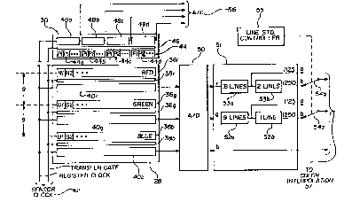
As further shown in ~igures 1 ~nd 2, the
unsharp color sensor 28 provides three channels of
color data to an analog-to-digital (A~D) converter
50, which digitizes the color data and ~pplies the
separate digitized channels to a color line
reyistration circuit 51. ~ecause the three color
arrays 36r, 369, 36b are spaced on the sensor 28 in
the (page or frame) direction of film motion, the
photosites being read at a different time correspond
to different vertical locations on the film frame.
This fi~ed mis-registration is corrected by the
color registration circuit ~1, which includes
suitable li~e delays 52a, 52b, and 53a, 53b, for
registering the color lines with each other and with
the luminance line. ln a film scanner of this type,
the spacing of the arrays 36r, 3Sg, 36b on the
substrate is generally selected to be an integral
num~er of scanning lines for a particular television
line standard.
~rom a sensor fabrication viewpoint a
minimum array spaciny required for a device to be
used on an 1125 line high definition system would ~e
8 lines or 91.13 microns on the film. ~Thi~
dimension is related to the sensor by multiplyi~g
this value by the optical magnification of the lens
W092/22988 PCT/US92/04861
2~92S -8-
system, which in this embodiment is approsimately
1.36 for Academy 35mm film format. All subsequent
dimensions discussed herein are also related to film
dimensions in the Academy 35 format. Identical
principles apply to other formats, ~nd no change in
sensor spacing or delay lines is required.) This
would ordinarily suggest the use of 8 lines of delzy
in the green channel and 16 lines of delay in the
red channel. If this sensor were to be operated on
the proposed European 'Eureka' standard of 1250
lines, without ~lter~tion in the num~er of vertical
delay elements used to register the signals,
~ertical color registration errors would result.
The ~ertical mis-registration of two signals from
adjacent color arrays would be equal to the arr~y
spacing (91.13 micron) minus 8 times the line
spacing of the 1250 line system (81.11 micron), sn
error of appro~imately 10 microns or almost one line
spacing. This is unacceFtably large, and would
result in visible color mis-registration. If,
h~wever, 9 lines of electronic delay are provided,
in accordance with the teaching of this invention,
when operating on the Eureka 1250 line standard the
increased delay is equivalent to 92.12 micron on the
film, and this is within 1.0 micron of the actual
sensor spacing. For the red and green signals the
error is now only appro~imately 10~ of the line
spacing. The red and blue arrays are separated by
twice the spacing of the red and green and will
produce twice the registration error.
The mis-registration on 1250 lines can be
further reduced by increasing the array spacing to 9
lines for 1125 operation, i.e. from 91.13 to 102.52
microns on the film. On the 1125 line standard 9
line delays will now be needed to register green to
W092/22988 ~ ~g 8 9 2 5 PCT/US92/04861
_g_
blue and 15 to register red to blue. For 1250 line
operation 10 lines will be needed for green to blue
and 20 for red to blue. The registration error
remaining on 1250 will be the difference between the
7 5 array spacing and 10 line spacing for 1250, i.e.
102.52-102.3~0.18 micron. This corresponds to 1.8
of a line spacing and will produce a visually
insignificant amount of vertical color
mis-registration. Figure 3 is helpful in showing
the substantially integral line multiples achieved
in each standard according to this invention.
As shown in Figure 2, 9 lines of delay are
provided by the delay 52a, and one additional line
of delay by the delay 52b, in the green channel.
Ei~hteen lines of delay are provided ~y the delay
53a, and two additional lines of delay by the del~y
53b, in the red channel. The outputs of the 9 and
18 line delays ~2a and 52b are directly connecte~ to
the poles a of ganged switches 54a and 54b while the
outputs of the combined delays ~2a and 52b (10
lines), and 53a and 53b (20 lines) are connected to
the poles b of the switches 59a and 54b. The
switches 54a and 54b are jointly controlled by a
line standard controller 55, which selects between
the 1125 or 1250 line standard and accordingly
directs the appropriate standard output for
subsequent processing.
When the line standard controller 55
selects one of the high definition line standards,
the line integration time of the respective color
sensors 36r, 369, 36b is accordingly changed to
produce the requisite number of lines (i.e., cither
1125 or 125C) during the transit period of a portion
of a film frame through the ,ilm gate 14, the
aforesaid portion having the correct aspect ratio
W~92/22988 PCT/US92/04861
2Q8~92S
--10--
for the given stand~rd (i.e., 16:9 for a high
definition standard). Since the line integrat~on
time is controlled by the g2ting signDl provided by
the sensor clock generator 42 to the linear CCD
arrays 36r, 369, 36b, a line 55a feeds a line
standard indication signal from the controller 55 to
the sensor clock generator 42.
As further shown in Figure 2, the lumin~nce
sensor 30 includes a linear array 44 sensitized to
light havin~ a ~pectral composition approsimating a
luminance function. The linear array 44 produces a
full resolution signal sufficient for the
requirements of either high definition st~ndard,
that is, the luminance array 44 includes a
sufficient number of active photosites so as to
correspond to the pi~el resolution of either high
definition standard. In this embodiment, the
luminance array in~ludes 1920 active photosites.
The array 44 is divided into four like-sized
segments q4a, 44b, 44c and 44d--each including a
subset Pl, P2,...of photosites; in this emb~diment,
there sre 480 acti~e photosites in each segment. A
transfer gate 46, connected to the sensor clock
generator 42, is ju~t~posed between the segments
44a, 44b, 44c, 44d and a corresponding plurality of
output shift registers 48a, 48b, 48c, 48d, which are
also connected to the sensor clock generator 42.
With such an architecture, the image charges in all
photosites in the array 44 are simultaneously gated
to the output registers 48a, 4Bb, 48c, 48d an~
simultaneously shifted therefrom at one-quarter the
clock frequency ordinarily needed for the high
definition dats rate, i.e., the data output r-te of
the luminance sensor 30 is four times the clock
freguency applied to the individual output registers
W092/22988 2 0 8 8 9 2 5 PCT/US92/04861
--11--
48a, 48b, 48c and 48d.
The ~ensors 28 and 30 are illustrate~ nest
to eDch other in Figure 2 to emphasize the relative
arrangement of the linesr arrays 36r, 369, 36b ~nd
44. It is of particular note that the color ~nd
luminance sensors 28 and 30 cover substantially the
same linear dimension, but with different
resolution. Low resolution, or unsharp, color is
provided from the color arrays 36r, 36g, 36b by
fewer photosites (960) than for luminance (1920).
As described in copending Serial No. 373,309, this
provides lower color resolution in the horizontal
scanning direction and allows the color photosites
to be accordingly larger, which has the advantageous
affect of increasing the signal-to-noise
performance. In a~dition, color resolution in the
vertical scanning direction is reduced by scanning
one line of color for every two lines of luminance,
thereby allowing the vertical color dimension to be
increased (doubled) in relation to the luminance
photosites. The total area of the color photosites
is ac~ordingly four times that of the luminance
photosites. Taking further into account that the
integration time of each color photosite is twice
that of a luminance photosite (because each color
line is read out half as freyuently), the signal
from the color photosites realizes an eight-fold
noise improvement.
The three color arrays 36r, 369 and 36b are
offset from each other by an integral number of
lines so that, at any instant, three separate lines
from the film 12 are imaged on the sensor 2~. With
the color arrays collecting light over a two (high
definition~ line period for each color line read
out, the color arrays are spaced by an integral
W092/229~X 2 0 8 8 9 2 5 PCT/US92/0486l
multiple of twice the high definition line spacing.
In particular, in the 1125 line standard the 9 line
spacing between the green array 36g and the blue
array 36b i5 equiv~lent to 18 luminance or high
definition lines, and the 18 line spacing between
the green array 369 and the red ~rray 36r is
equiv~lent to 36 luminance or high definition
lines. Similarly, in the 1250 line standard, the 10
line spacing corresponds to 20 luminance or high
definition lines and the 20 line sp2cing corresp~nds
to 40 luminance or high definition lines. The
luminance sensor 30 may be aligne~ to a fourth,
separate line or, via the beam splitter 26, to one
of the color lines, say the line imaged upon the
green-sensitive array 36g. The horizontal (line)
scan is provided ~y transferring image charge from
the linear arrays to the output registers, an~
accordingly clocking the signals from the
registers. The vertical (frame) scan is provided by
the motion imparted to the film 12 by the film
transport 10 (Figure 1), and allows for the
requisite lines in a frame.
As described in copending Serial No.
373,309, the luminance segments 4qa, 44b, 44c, 44d
are structured relative to the color 2rrays 36r,
36g, 36b so that the number of photosites in a color
~rray is an integral multiple of the num~er of
photosites in a luminance segment. As described
herein, each color array has twice as many
photosites as a luminance segment; specifically,
each color array 36r, ~69, 36b has 960 photosites in
relation to 480 photosites for each luminance
segment 44a, 44b, 44c, 44d. The luminance registers
q8a, 48b, 48c, 48d are read in parallel once for
each line while the color registers qOr, 40g, 40b
wo 92/22g~ 2 0 8 8 9 2 5 PCT/US92/~KI
. .
-13-
are read in parallel once for every two lines of
luminance. Since there are twice a$ many photosites
per register in~color as in luminance and the color
is read half as frequently, the numbers of
photosites read per second is the same for colcr and
luminance; consequently, or.ly a single clock
frequency is re~uired to read out all of the
reQisters 40r, 409, 40b, 4Ba, 4Bb, 46c, 48d.
Referring again to ~igure 1, the lu-in2nce
sensor 30 provides four channels of luminance data,
one from each register 48a, 4Bb, 48c, 4Bd (Fig. 2),
to plural analog-to-digital (A~D) eon~erters shown
as block 56. Depending on the re~istration cf the
lu,,.inance line relative to the color lines, a line
dela~ may be inserted into the luminance channel(s)
to re~ister the luminar.ce lines with 4 selected
color line. Since the digital color values
represent lower re~olu'iofi data than the digital
lu~inance alues, additior.al color values are
Qene-ate~ in a color i-nterpolation circuit 57 in
b^th the horizon'al and vertical directions.
~;canhhile, high freguênc~ detail is estracted fro...
thC four channels of lumir.2nce data b~ a d~
eJ.traction circuit 58, whieh includes an arra~ of
high pass filters (not shown). The signals in the
four lu~inance chanr.els are alisnei ~end-t~-e~d~ to
correspond to a physieal line in a reformat circuit
60, which ma , for exa~ple, be a conventional
multiplexer trig~ered in quarter-line se~uence tc
output a continuous detail signal.
~ he detail is a~ded to each channel of
color in an addition circuit 62, forming thereafter
a full res~lution, high definition color output
signal. This high definitio.l output signal is
applied to an image store 64, which includes a first
W092/22988 PCT/US92/04861
2088~S - ~.
-14-
framestore 64a and 2 second framestore 64b.
Recalling now that the high definition signal to
this point is a seguential signal, an interl-ce
controller 66 loads a video frame sequentially ~nto
one framestore while estracting video fields (of
previously loaded frame) in interlace format from
the other framestore. A digital red, qreen, blue
high definition field signal is thus provided ~t the
output of the image store 64 for further use, which
may include immediate broadcast transmission or
recording, e.g., on video tape (after suitable
standards conversion or encoding, as necessary). In
any event, such further use is not to be part of the
present invention.
An alternative embodiment of the high
resolution luminance sensor 30 is shown in ~igure 4,
and described more fully in Serial Number 422,254,
filed October 16, 1989 in the name of H. J. Erhardt,
assigned to the same assignee 25 the present
invention, and incorporated herein by reference.
(S.N. 422,254 is a commonly owned application for
which the issue fee has been paid.) As further
shohn in Figure 4, the luminance sensor 30 includes
four like-sized segments 140a, 140b, 14~c and
140d--each including a subset of a full line of
photosites; in this embodiment, there are 480 active
photosites in each subset plus four outer photosites
at either end thereof. The segments are supporte~
on the sensor s~bstrate such that adjoining ends
overlap by eight photosites (including the four
outer photosites), defining an overlap region 141
between segments 140a and 140b, 140b ~nd 140c, an~
140c and 140d. Each full line output thus consists
of partial lines of signals ~rom the four segments
~5 140a, 140b, 140c, and 140d joined together at
W092/22988 2 ~ $ ~ 9 2 S PCT/US92/04861
-15-
crossover points indicated by the arrohs c in ~igure
4. ~our transfer gates 142a, 142b, 142c and 142d
are ju~taposed between the segments 140a, 140b,
140c, and 140d and a corresponding plurality of
output shift registers 144a, 144b, 144c, and 144d.
By staggering the linear segme~ts and
overlapping adjoining ends thereof as described in
copending S.N. 422, 254, the sampled signal outputs
of the several segments can be applied to a series
of digital filters that operate independently to
provide filtered output signals that can ~e grDuped
together without processing artifacts at the
crossover points. More particularly, the
overlapping regions of the linear segments are
configured in relation to the processing kernal
required by the digital filters such that
contiguous, processe~ samples on either side of each
crossover point are derived from sample strings
wholly within a respective linear segment.
The linear segments 140a and 140c are
offset from the linear seQments l~Ob and 140d by an
integral number n of lines so that, at any instant,
two separate lines from the film 12 are imaged by
the objective lens 2~ on the sensor 30. In
accGrdance with the present invention, the integral
number n can be chosen to also correspond to a
substantially integral multiple of two television
line standards. ~or e~ample, n can be established
at 9 luminance or high definition lines of the 1125
line standard, and also be substantiall~ equivalent
to 10 luminance or high definition lines of the 1250
line standard. Corresponding integral multiples ~f
line delays in the respective channels, as described
in connection with the color linear sensor 28, can
then be used to select the output signals according
W092/22988 J PCT/US92/04861
2~g3~ 16-
to the standard in use. More particularly, a
detail registration circuit (not shown), ~irectly
analogous to the color registration circuit 51,
would be provided in the separate luminance channels
with a ganged switch (analogous to switch 54 tFigure
2)) for switching between the standards accordinq to
output from the time standard controller 55.
The invention has been described in detail
with particular reference to a presently preferred
1~ embodiment, but it will be understood that
~ariations and modifications can be effected within
the spirit and scope of the in~ention. In
particular, while the invention has been described
for use in connection with high definition line
standards, it is egually useful with other line
standards. Moreover, line scanning apparatus
according to the invention could also be adapted to
more than two television standards, say, three high
definition stan~ards, by appropriate spacing egual
to substantially integral multiples of all three (or
more) standards.