Note: Descriptions are shown in the official language in which they were submitted.
2~~~~1'~
METHOD AND APPARATUS FOR
INSPECTING A PRINTED CIRCUIT BOARD
Backqround of the Invention
This invention relates generally to systems for
inspecting printed circuit boards, and more particularly, to an
improved system for analyzing successive viewing fields at an
increased rate.
As is well known to persons skilled in the art, a
printed circuit board is used for mounting and electrically
interconnecting electrical components in a predetermined manner.
To the extent possible, such printed circuit boards are
l0 constructed mechanically, using automated assembly machines which
operate to reduce t:he often prohibitive costs of manually
assembling a printEad circuit board. While reducing overall
costs, such automated assembly techniques have been found to give
rise to a certain 7_imited number of assembly defects such as
incorrect insertions of components, and their leads or pins, as
well as defects in the soldering procedures which then follow.
Original7Ly, steps were taken to locate assembly errors
of this general type through a visual inspection of each printed
circuit board at a desired stage of the manufacturing process, by
human operators using the naked eye, or possibly a stereo
microscope or the .Like. However, since this procedure was found
uw oFC~cEs
wE~s~.~S7APLERtO be extremely tedious and inaccurate, as well as a relatively
s~ s
~p $Q HG'TEENT~1 ST
PHIV1DELPMA PA o9n02
~:~s~e~s.a~ _ _
tE~ECOP~EN ~2 ~ 5) e75d79.
20~~~~"~
expensive process, steps were taken to develop automated systems
for inspecting printed circuit boards, to replace such visual
inspections.
Examples of devices of this general type are the Model
5511, Model 5512, Model 5515, Model 5516 and Model 5517 Printed
Circuit Board Inspection Systems which are manufactured by
Control Automation Incorporated of Princeton, New Jersey. These
inspection devices generally employ a series of cameras which are
mounted within a fixture (an inspection head) adapted for
controlled movement: relative to a printed circuit board. The
inspection head is either sequentially advanced to successive
viewing fields (typically one inch by one inch) established along
the surface of the printed circuit board then under inspection,
or continuously advanced along the surface of the printed circuit
board, to acquire images for microprocessor analysis. Any
detected defects are in turn reported to the operator, for
appropriate correction.
Such dev~~ces operate to enhance the accuracy of the
inspection process by providing an inspection head which
incorporates a series of four angled, orthogonally placed
cameras, operated in conjunction with a selectively controllable
light source. Through selective control of this series of
cameras, and the associated light source, a variety of testing
procedures are enabled including a verification of the placement
of components (and their leads or pins), both before and after
Uw OFFICES
wE~SQ.~sT,.~xthe soldering procedure, as well as a verification of the solder
SJITE 500
Z~p $Q FIFTEENTH $T
P~A,ADELP"IIA PA 19102
(2'~51 ETSd'HJ
rEmcoPIEA u~s~ eTS.a3s. -2 -
connections which .are made.
Initially, such inspections were accomplished by
sequentially advancing the inspection head (or the printed
circuit board) thr~~ugh successive viewing fields, and by
selectively activating the series of cameras and their associated
lighting to acquire images for inspection purposes. Later,
primarily in order to increase the rate at which circuit board
inspections could :be accomplished, such inspections were
accomplished by continuously advancing the inspection head (or
the printed circuit board) through its successive viewing fields,
and by selectively strobing the associated lighting system to
acquire images for inspection purposes. However, even this
enhancement was found to have certain limitations in terms of the
rate at which printed circuit boards could be inspected,
primarily resulting from limitations associated with the video
systems which were employed.
In overall operation, the continuous inspection of a
printed circuit board involves scanning of the board in a given
direction and at a rate which allows three successive functions
to take place including scanning, frame storage and processing.
Such techniques, which are often referred to as "pipelining", are
primarily limited by the rate at which video images are acquired
by the video cameras during the scanning portions of this
procedure. The primary reason for this is that conventional
video formatting (for the cameras and for display on a monitor)
uw OF: (CEs
wE~sE~~sT~~~operates within a specified bandwidth, to develop images which
sulTE sx
2~p s0 FnTEEr~'~ ST
AILAOEJ..°mA VA '9'.02
(1'.51 BTS-BJN ~
TELECO~EA 12'57 L75d79. ~ .7
e.~
are "interlaced" so that changes in the image from frame to frame
are less noticeable to the human eye. To this end, the series of
lines which conventionally comprise a video image are operated
upon in alternating' fashion so that a first series of alternating
lines (generally referred to as the "odd field") is acquired
and/or processed, followed by the acquisition and/or processing
of a second series of alternating, interlaced lines (referred to
as the "even field"). Resulting from this, the successive
(odd/even) fields of a video image are combined to develop a
complete frame for subsequent processing, all of which must be
accomplished within the operative bandwidth for the system.
Consequently, a period of 33.3 milliseconds is
generally required to develop a single frame of video
information, for subsequent storage and processing (allowing 16.7
milliseconds for processing the odd and even fields,
respectively). ThEa rate at which printed circuit boards can be
inspected by existing equipment is correspondingly limited by the
rate at which video images can be acquired (i.e., at 33.3
millisecond intervals). For a conventional viewing field
(typically one inch by one inch), this limits the rate at which
circuit boards can be inspected to approximately 15 inches per
second. The reason for this is that the views which are to be
acquired by the series of cameras associated with the inspection
apparatus are over:Lapped by 50% (with paired cameras utilizing
different lighting modes). As a consequence of this, the
Uw OFFICES
wE~s~.~sT~P~~inspection head muat travel one-half inch (for each pair of
SLATE 500
Zp 5p RFTEErfTH ST
pH~E~,A1N,PAn9lp~ cameras) in 33. 3 milliseconds, or 15 inches per second.
carn eTS.ex~
fELECORiER (7I5) 875-039.
-4-
20899 17
Summary of the Invention
It is therefore a primary object of an aspect of the present invention
to provide a method and apparatus for inspecting printed circuit boards at
an increased rate.
It is also an object of an aspect of the present invention to provide a
method and apparatus for inspecting printed circuit boards at an
increased rate making use of existing video cameras, and video processing
systems.
It is also an object of an aspect of the present invention to provide a
method and apparatus for inspecting printed circuit boards at an
increased rate which can virtually double the rate of inspection while
maintaining the formatting which is necessary for processing and
displaying video images.
These and other objects are achieved in accordance with the present
invention by providing a method and apparatus for inspecting printed
circuit boards which doubles the transport rate for the printed circuit
board, and which modifies the manner in which acquired video images
are processed to account for this change in rate. Primarily, this involves
two modifications. to existing video processing systems including a change
in synchronization for obtaining the frames which are to be processed, and
a selective exposure (i.e., shuttering) of the video cameras to the images
which are to be acquired in order to avoid the acquisition of plural images
in a single frame. Once acquired, the video images are stored and
processed making; use of
-5-
F 208g9~ ~7
techniques which substantially correspond to those previously employed
by existing printed circuit board inspection devices.
Other aspects of this invention are as follows:
An apparatus for inspecting an article, comprising:
a head for inspecting regions defined on the article;
a plurality of cameras coupled with the inspecting head, wherein at
least a first one of the cameras is operated responsive to a first
synchronization signal and at least a second one of the cameras is operated
responsive to a second synchronization signal, and wherein the second
synchronization signal is delayed relative to the first synchronization
signal;
means for selectively illuminating the regions defined on the
article; and
means for selectively exposing the plurality of cameras to images
resulting from selective operations of the illuminating means.
A method ~Eor inspecting an article with an apparatus including a
head for inspecting regions defined on the article, and a plurality of
cameras coupled 'with the inspecting head, wherein at least a first one of
the cameras is operated responsive to a first synchronization signal, and at
least a second one of the cameras is operated responsive to a second
synchronization signal, the method comprising the steps of:
delaying the second synchronization signal relative to the first
synchronization s ignal;
selectively illuminating the regions defined on the article; and
selectively exposing the plurality of cameras to images resulting
from selective operations of the illuminating means.
For further detail regarding a preferred embodiment method and
apparatus produced in accordance with the present invention, reference is
made to the detailed description which is provided below, taken in
conjunction with i:he following illustrations.
-6-
. 20899 ~7
Brief Description of the Drawings
Figure 1 is an isometric view of the inspection head of a printed
circuit board ins~~ection device.
Figure 2 is a block diagram of a system for acquiring images, and
for processing them acquired images, in accordance with the present
invention.
Figure 3 is a schematic view of a delay circuit for the system which
is illustrated in Figure 2.
Figure 4 is a timing diagram for the system which is illustrated in
Figure 2.
In the several views provided, like reference numbers denote
similar structures.
-6a-
Detailed Description of the Preferred Embodiment
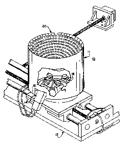
Figure 1 generally illustrates an apparatus 10 for
inspecting printed circuit boards (not shown) in accordance with
the present invention. The apparatus l0 generally includes an
inspection head 11 which is supported for predetermined movement
in a defined plane by an X-Y table (generally designated by the
reference number 12), using any of a variety of known servomotor
controls. The inspection head 11 further includes a plurality of
TV or video cameras 13, 14, 15, 16, and a lighting fixture 20 for
l0 selectively illuminating regions on the printed circuit board so
that appropriate images may be acquired by the video cameras 13,
14, 15, 16. Further detail regarding the basic construction of
the apparatus 10, its various components, and its manner of
operation, may be had with reference to U.S. Patent No.
5,060,065.
Referring now to Figure 2, .images acquired by the
cameras 13, 14, 15, 16 are converted to electrical signals (video
outputs) which are respectively delivered at 21, 22, 23, 24. The
video outputs 21, 22, 23, 24 in turn communicate with a series of
frame storage units 25, 26, 27, 28 which operate to receive and
temporarily store the video signals for subsequent processing.
To this end, the frame storage units 25, 26, 27, 28 communicate
with central processing units 29, 30 via an information buss 31.
Resulting from this, images acquired by the cameras 13, 14, 15,
uw OFSiCEs
WEIS~~STAPLER16, and stored within the frame storage units 25, 26, 27, 28, can
$~rtE 500
~~0 5p FnFTEEHTH 5T
F-~K,ApEL~~A. DA n9'02
u's~e~sa~
rELECO. ~En ~x~ sr eTSa~s. - 7 -
be selectively accessed and processed by the central processing
units 29, 30, as desired. Means for implementing these
structural components, and for processing the information which
is acquired, are known from prior circuit board inspection
devices which employ similar structural components and processing
techniques. Accordingly, further detail regarding these
components is unne~~essary to a full understanding of the present
invention, other tlhan to describe the interaction of such
components with thte improvements of the present invention.
In accordance with the present invention, steps are
taken to, in essence, double the rate at which circuit boards are
inspected by doubling the transport speed for the X-Y table 12,
and by modifying t:he manner in which video images are acquired.
Thus, in analyzing typical viewing fields measuring one inch by
one inch employing previously known techniques, the X-Y table 12
would conventionally be caused to traverse 0.5 inches in 33.3
milliseconds during operations of the cameras 13, 15, and another
0.5 inches (in another 33.3 milliseconds) during operations of
the cameras 14, 16 (which are overlapped by 50%). This produced
a transport velocity of approximately 15 inches per second.
During this period of time, steps would be taken to acquire an
image for storage and subsequent processing, subject to the
timing requirements for acquiring video images employing
conventional video cameras. In accordance with the present
invention, the transport velocity is doubled, to approximately 30
uw oFF~cEs
wE~sa.~sT~P~~inches per second. However, this has the corresponding effect of
suiTE soo
zip 50. FIF1I:EVTY $1
pn[~7E/ V~lu iA ~ 9t p~
i:~si e~sa~~
Tmcoo~Ep wsi eTS-e3x
2~u9~~.'~
reducing the period of time available for acquiring video images
by one-half, to approximately 16.7 milliseconds. This then
requires certain modification of the overall video processing
scheme which is employed.
For example, even though the video intervals
established by the method and apparatus of the present invention
are reduced by one-half, the video intervals associated with the
otherwise conventional video cameras will remain at their normal
rate. Resulting from this, the video cameras 13, 14, 15, 16 must
now operate in opposing (odd/even) fields. This is because while
the cameras 13, 15 are operating in the even field, the cameras
14, 16 will be operating in the odd field, and vice versa.
However, it is necE;ssary for the lighting fixture 20 to be
strobed while each of the cameras are in their odd field for
proper processing of the video signals which are to be produced.
Since the cameras :L3, 15 and the cameras 14, 16 are now out of
phase by 180° (i.e., 16.7 milliseconds apart), steps must
therefore be taken to correct this timing. In accordance with
the present invention, this is accomplished by delaying the
horizontal synchronization for the cameras 14, 16 relative to the
cameras 13, 15 by one-half of a horizontal line.
To this end, the horizontal synchronization signal 36
received from the :frame storage unit 25 associated with the
camera 13, which serves as the master frame storage unit, is
delayed prior to application to the frame storage units 27, 28
Uw OFFICES
wE~~~sT~~Rassociated with thle cameras 14, 16. This is accomplished by a
S:IITE S00
j~p $~ FIFTEENTH 5T
PN4ADElPNtA PA ~9lpj
n,sleTS.e~e~ _ _
TELECOPIEP f2~51 875-079.
.. 2~~9~~7 ~..
delay circuit 35 which is configured to establish the one-half
horizontal line delay which is desired.
Thus, as shown, the horizontal synchronization signal
36 received from the frame storage unit 25 (master) is coupled
with the frame storage unit 26, at 37, maintaining the frame
storage units 25, ~:6 associated with the cameras 13, 15 in
synchronization. However, the horizontal synchronization signals
38, 39 for the frame storage units 27, 28 are first subjected to
operations of the delay circuit 35, producing the one-half
horizontal line delay which is desired for the cameras 14, 16
(which are associat=ed with the frame storage units 27, 28). The
position of the horizontal synchronization signals 36, 37, 38, 39
relative to the vertical synchronization signal 34 then
determines (identil:ies) the odd and even fields. Similar
modifications are also made to the master synchronization unit
40, which communicates with each of the frame storage units 25,
26, 27, 28, for ove=rall synchronization purposes.
The mastE~r synchronization unit 40 substantially
corresponds to sim=ilar units used in existing circuit board
inspection devices, modified to accommodate the one-half
horizontal line de:Lay developed by the delay circuit 35. Any of
a number of known delay circuits may be employed to implement the
delay circuit 35. However, a particularly desirable result is
achievable by employing the recirculating delay line circuit 35'
which is shown in :Figure 3 of the drawings. In this
Uw OFS~CES
WEISEl4STAPLERCOnflgur~atiOn, the horizontal synchronization signal 36 is
SUrtE 500
27p 5p FIFTEENTH 5t
p.,MpE~pNU, vA n9n07
(3~5> 815-070.7 _
tEI_ECOW ER (2151 !75d79. 1 ~
..
introduced into a shift register 41 (e. g., a 128-bit shift
register) and a counting circuit 42 (e. g., a 3-count shift
register). Clock signals 43 for operating the shift register 41
are derived from the horizontal synchronization established for
the overall video processing system. Following operations (a
first count) of the shift register 41, the counting circuit 42 is
advanced, and the shift register 41 is caused to produce a second
count. Following this, the counting circuit 42 is again
advanced, and the shift register 41 is caused to produce a third
count. This, in turn, activates a gating circuit 44, which
corresponds to a delay equal to one-half of a horizontal line, as
is desired.
Yet another consideration resulting from conventional
video formatting i~; that the acquired image, and the resulting
signal, is integrated through interlaced first (odd) and second
(even) fields. The acquired images (signals) are output
serially, leading with the odd field and followed by the even
field. However, each field requires 16.7 milliseconds to be
transferred from tree camera to its respective frame storage unit.
In conventional sy:>tems, having the entire 33.3 millisecond
period for acquiring a single image, strobing of the lighting
fixture 20 did not result in any interaction between the video
images (odd/even) acquired by the cameras 13, 14, 15, 16. In
strobing the cameras 13, 15, images would also be received by the
cameras 14, 16. However, this occurred during a period when
Uw OFFICES
wE~sE~~st~r~Roperations of the cameras 14, 16 could simply be ignored
s~
=gyp $~ FIFTEENT~1 $1
P.iLADELGN1A. PA n9tp~
ats~ eTS.ex3
-E~coP~Ea ~atsi e>sa~s. -11-
n
(blanked), eliminating such secondary images.
Reducing the operative video interval to 16.7
milliseconds results in the production of secondary images which
can no longer be il~nored, since they are no longer produced
during a dormant operating period. Because of this, strobing of
the cameras 13, 15 will result in a secondary image in the
cameras 14, 16, and vice versa, which will not be automatically
eliminated through operations of the cameras. Instead, resulting
from the accelerated timing established in accordance with the
present invention, these secondary images will interfere with
desired operations of the cameras.
For this reason, and in accordance with the present
invention, each of the cameras 13, 14, 15, 16 are provided with a
shutter 45, 46, 47, 48, respectively, which can be selectively
operated to eliminate secondary images received during strobing
of the opposing cameras in even fields. Synchronization for the
shutters 45, 47 is received from the frame storage unit 27,~at
49a, and synchronization for the shutters 46, 48 is received from
the frame storage unit 25, at 49b. By closing the shutters of
any cameras which are then in their even field, undesirable
secondary images are effectively eliminated.
The shutters 45, 46, 47, 48 are preferably liquid
crystal shutters, since such shutters are sufficiently fast and
resilient to withstand the operations which are required to
effectively control the images acquired by the cameras 13, 14,
uW ~F~Es
wE'S~'STA~~15, 16. An example of a liquid crystal shutter of this general
$;117E 500
j~p $Q FIFTEENTH $T
P-IaADELiHIw. PA n9o02
(j'S16TSd7o0
rE, E :oolEa u~ 51 eTSa3s. ~ 12
type is the Model hV050P "light valve" which is manufactured by
Displaytech, Inc. of Boulder, Colorado. These shutters can
operate at speeds :Ln excess of 50 microseconds, a speed which is
sufficiently fast 1~o meet the needs which are required of them.
In operation, and referring now to Figure 4 of the
drawings, it will he assumed that the circuit board inspection
apparatus 10 is operating so that the X-Y table 12 (Figure 1) is
causing the inspeci~ion head 11 to traverse a printed circuit
board at an increased rate of speed which is achievable in
accordance with the present invention (e.g., 29 inches per
second). Responsible to synchronization signals received from the
frame storage units 25, 26, 27, 28, and the master
synchronization unit 40, the cameras 13, 14, 15, 16 will commence
the acquisition of images and the conversion of such images to
electrical signals 21, 22, 23, 24. Waveforms 50, 51 of Figure 4
schematically illustrate operation of the video cameras as they
progress through this video acquisition process.
To be noted is that the cameras 13, 15 of waveform 50,
as well as the cameras 14, 16 of waveform 51, are operated during
alternating 16.7 millisecond intervals, as distinguished from the
33.3 millisecond intervals which were previously conventionally
utilized. Also to be noted is that the cameras 13, 14, 15, 16
are operated in conjunction with their corresponding shutters 45,
46, 47, 48, according to the waveforms 52, 53 which are
illustrated in Figure 4. The waveform 52 shows operation of the
uw o~Kes
wE~s~~sT~~xshutters 45, 47 which are associated with the cameras 13, 15,
SUITE 500
~p $Q FIF-~VTr1 5T
pH~,.,~~N iA 19'~02
a s~ e~saxa
rELECOOrta :r s~ e~s-ess. -13 -
2'~8~~~.~
while the waveform 53 shows operation of the shutters 46, 48
which are associated with the cameras 14, 16.
Operations of the video cameras, and their associated
shutter mechanisms, are performed in conjunction with strobed
operations of the lighting fixture 20, as is illustrated by the
waveforms 54, 55 of Figure 4. It will be noted that strobed
operations of the lighting fixture 20 in conjunction with the
cameras 13, 15 (wav~eform 50) occur when the associated shutters
45, 47 are open (waweform 52). Similarly, strobed operations of
the lighting fixture 20 in conjunction with the cameras 14, 16
(waveform 51) occur when the associated shutters 46, 48 are open
(waveform 53). Although the strobed operations represented by
the waveforms 54, °_.5 are shown to occur substantially midway
within the active operational periods which are shown, other
timing configurations may also be developed within the 16.7
millisecond "windows" which are established in accordance with
the present inventpon.
Resulting from this, framed images are transferred to
the frame storage units 25, 26, 27, 28, storing successive video
images represented by the waveforms 56, 57, 58, 59. These images
are then accessed by the central processing units 29, 30, for
interpretation using techniques which are in and of themselves
known, and employed in prior circuit board inspection systems of
this general type.
Such processing will continue until the entire surface
uw OFFICES
we~s~.~sT~r~~of a printed circuit board is inspected. Following this, the X-Y
Z~p 5p FIFT[ENTVI $T
p.p~pNIA. PA l9nQ~
f2~51 815-0781
TELECOPffR f3 n 51 !75d79. 1 4 -
table 12, as well as the frame storage units 25, 26, 27, 28, are
returned to their initial state, readying them for inspection of
the next printed circuit board to be operated upon. During this
period of time, the horizontal delay earlier established by the
delay circuit 35 is discontinued in order to facilitate operator
functions (i.e., user menus, operator interfaces, and video
displays on the monitor associated with the printed circuit board
inspection system). This is necessary since the desired video
images could not otherwise be displayed on a monitor due to the
changes in synchronization which are developed by the delay
circuit 35.
To this e:nd, and referring again to Figure 3, a second
gating circuit 60 is provided which receives as its input 61 a
conventional (without delay) synchronization signal from the
apparatus 10. Application of a control signal, at 62, operates
to deactivate the dating circuit 44 and to activate the gating
circuit 60, removing the delay established by the delay circuit
35 when desired. :signals received from the gating circuits 44,
60 are combined at 63, for subsequent interaction with the
remainder of the printed circuit board inspection apparatus l0 as
desired.
It will 'therefore be understood that various changes in
the details, materials and arrangement of parts which have been
herein described a:nd illustrated in order to explain the nature
of this invention :may be made by those skilled in the art within
uw oF~lr~s
wE~s~~sr~r~.E~the principle and scope of the invention as expressed in the
Su~E s
=gyp 5p. FIFfEENIH $T
Pr1[,~E~PrIIA. OA X9002
cx~s~ eTSax~
TE~cov~En a~si e~saas. -15 -
._
following claims. For example, although the above description of
a preferred embodiment device addresses the inspection of printed
circuit boards, the method and apparatus of the present invention
may similarly be employed to inspect other articles, such as
manufactured parts or the like. Other applications will become
readily apparent to the skilled artisan.
uw oFF~cEs
WELSER /t STAPLER
S:J~TE 500
2J0 50 FiFTEEYTH ST
P..vpE~y~n,~ Pa ,9,0Q
(2'.51 B75~JlJ
rELEcov~En u,sl eTS aTS~ -16 -