Note: Descriptions are shown in the official language in which they were submitted.
2~014~
SEI 92-38
1 TITLE OF THE lNv~NlION
Photodetector
BACKGROUND OF THE INVENTION
Field of the Invention
This invention relates to a photodetector for use in
light output monitoring devices of semiconductor lasers,
receiving devices of optical communication systems, etc.
Related Background Art
FIG. lA is a top view of a structure of a conventional
light detecting element, and FIG. lB is a sectional view
along the line X-X' in FIG. lA. As shown, the conventional
light detecting element comprises a first conduction-type
semiconductor substrate 1 with a first electrode 8 formed
on the underside; a first conduction-type semiconductor
crystal layer 2 including a light absorbing layer; and a
second conduction-type first region 3 formed in the first
conduction-type semiconductor crystal layer 2 by
- selectively diffusing a dopant. Thus formed is a pin
photodiode structure. This pin photodiode structure
includes an n-layer (or a p-layer) provided by the
semiconductor substrate 1, a p-layer (or an n-layer)
provided by a first region 3, and a light detecting region
10 provided by the pn junction (the depletion layer or the
i layer). A second electrode 5 is provided on the first
region 3 in the semiconductor crystal layer 2. The top of
the first region 3 inside the electrode 5 is covered with a
209014~
SEI 92-38
1 reflection preventive film 6, and the top of semiconductor
crystal layer 2 outside the electrode 5 is covered with a
device protective film 7.
In the semiconductor device of the above-described
structure, when an reverse bias is applied, an electric
field is generated in the depletion layer. Electrons and
holes generated by incident light on a light detecting
region 10 are devided respectively to the first conduction-
type region 3 and are accelerated. Thus a photocurrent can
be taken outside. And an optical signal can be detected.
In the above-described structure of FIG. lA and lB, when
light is incident on the light detecting region 10, photo-~
carriers are generated in the depletion layer, and a good
response characteristic can be obtained. But when light is
incident outside the light detecting region 10, due to
density gradient the generated carriers are diffused to
reach the depletion layer, and are taken out in a
photocurrent. The transfer of the diffused carriers is
slow. When the carriers reach the light detecting region
10, adversely a tail is generated at the last transition of
a light-pulse-responding waveform as shown in FIG 2.
In using such light detecting element in photodetectors
for use in optical communication, etc.,
a lens 11, such as a spherical lens, a SELFOC lens or
others, is disposed at the light incident part of the cap of
the package as shown in FIG. 3 so as not to affect the
209~
SEI 92-38
1 response characteristic. This arrangement enables all the
signal light emitted from an optical fiber or others to be
focussed to be incident on the light detecting region 3.
But this condensation increases an incident light intensity
per a unit area of signal light incident on the light
detecting region 3, and accordingly more carriers are
generated in the depletion layer 10. Resultantly because
of the space-charge effect produced by an increase of a
carrier density in the depletion layer 10, an intensity of
an electric field in the depletion layer 10 is decreased,
and a drift rate of the carriers in the depletion layer 10
is lowered. Also tails occur at the falls of light pulse
response waveforms. In view of this, the light amount to be
incident on the light detecting element 20 has to be
limited, and it is a problem that a maximum incident light
amount on the semiconductor photodetector cannot be
increased. This effect is more conspicuous especially when
the reverse bias voltage is low, which makes it difficult to
operate the semiconductor photodetectors at low bias
voltages.
In controlling a light output of a laser diode to be
constant, the light emitted from the rear end surface of the
laser diode is detected by a light detecting element, and an
operating current of the laser diode is feed-back
controlled. But because the light output of the laser diode
is so intense that when light is focussed and incident on
2~901~
SEI 92-38
1 the light detecting region 3, the space-charge effect
occurs, and as described above, the drift of the carriers is
increased, and tails occur at the falls of response
waveforms. The feed-back control of the laser diode is
affected.
SUMMARY OF THE INVENTION
An object of this invention is to provide a
semiconductor photodetector which can solve the above-
described problems.
To this end, a photodetector according to the present
invention comprises a package in which a window is provided
in a light incident portion, a light detecting elements
located within the package, the light detecting element
comprising: a first region formed of second conduction-type
semiconductor and embedded in a first conduction-type
semiconductor layer; a second region formed of second
conduction-type semiconductor and embedded so as to be
spaced from and surround the first region; and a conductor
layer provided both on at least one part of top surface of
the first conduction-type semiconductor layer and on at
least one part of top surface of the second region.
In the semiconductor photo-detecting device, a window
provided in the package is a simple through hole and any
lens is not used in the package. A signal light, therefore,
is not concentrated in a light receiving region of the
photo-detecting element and the signal light is also
209014S
SEI 92-38
1 incident on an outside of the light receiving region. As
the result, an intensity of the signal light incident on the
light receiving region decreases and it may be prevented to
degrade the response characteristics due to space charge
effect. Further, it may be to make signal light having
large intensity incident into the photo-detecting device
without limiting the amount of the signal light.
Further, the similar effect may be also realized in
using a transparent plate in the light incident portion.
According to the above-described light detecting
element, even if incident light leaks outside the light
detecting region which is the pn junction formed between the
first conduction-type semiconductor layer and the first
region and adversely generates carriers, the carriers are
absorbed by the second region with the result that the flow
of the diffused carriers into the light detecting region can
be prevented. Consequently a necessary photocurrent alone
can be taken out to an outside circuit. Decrease of a
response speed of the device can be prevented.
The first conduction-type semiconductor layer and the
second region is short-circuited by a conductor layer of a
metal, a semiconductor or others formed over their top
surfaces, and carriers absorbed by the second region can be
recombined or extinguished. Accordingly carriers are not
accumulated in the second region. Even when light pulse of
very high intensities is incident, no tail is generated at
2090~ 4~
SEI 92-38
1 the last transition of a response waveform for the light
pulse. Thus, electric and optical characteristics of the
device can be improved.
The present invention will become more fully understood
from the detailed description given hereinbelow and the
accompanying drawings which are given by way of
illustration only, and thus are not to be considered as
limiting the present invention.
Further scope of applicability of the present invention
will become apparent from the detailed description given
hereinafter. However, it should be understood that the
detailed description and specific examples, while
indicating preferred embodiments of the invention, are
given by way of illustration only, since various changes and
modifications within the spirit and scope of the invention
will become apparent to those skilled in the art form this
detailed description.
BRIEF DESCRIPTION OF THE DRAWINGS
FIG. lA is a plan view of a light detecting element used
in a conventional photodetector explaining the structure
thereof.
FIG. lB is a sectional view of the light detecting
element along X-X'.
FIG. Z is a graph of the light pulse characteristic of
the conventional light detecting element.
FIG. 3 is a sectional view of the conventional
209014~
SEI 92-38
1 photodetector explaining the structure thereof.
FIG. 4A iS a plan view of a light detecting element for
use in the photodetector according to a first embodiment of
this invention.
FIG. 4B iS a sectional view of the light detecting
element along X-X'.
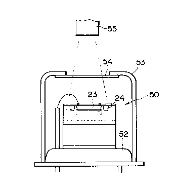
FIG. 5 is a sectional view of the photodetector
according to a second embodiment of this invention.
FIG. 6A iS a plan view of a light detecting element for
use in the photodetector according to the second embodiment
of this invention.
FIG. 6B is a sectional view of the light detecting
element along X-X'.
FIG. 7A iS a plan view of a light detecting element for
use in the photodetector according to a third embodiment of
this invention, which explains the structure thereof.
FIG. 7B iS a sectional view of the light detecting
element along X-X'.
DESCRIPTION OF THE PREFERRED EMBODIMENTS
A first embodiment of this invention will be explained
with reference to FIGs. 4A and 4B, and FIG. 5. FIG. 4A is
a top view of the light detecting device according to the
first embodiment, and FIG. 4B iS a sectional view along the
line X-X'. On an n~InP (Indium-Phosphide) semiconductor
substrate 21 with an n-electrode 28 formed on the underside,
there are formed a non-doped InP buffer layer 22a (carrier
2 0 ~
SEI 92-38
1 concentration: n=2xlO15cm-3, thickness: 2 ~m), a non-doped
InGaAs (Indium-Gallium-Arsenide) light-detecting layer 22b
(n=3xlOl5cm~3, thickness: 3.5 ~m), and a non-doped InP window
layer 22c (n=lxlO15cm~3, thickness: 2 ~m) for decreasing a
dark current. In the light detecting layer 22b and the
window layer 22c, there are formed a p-type first region 23
and a p-type second region 24 by selectively diffusing Zn.
The first region has a 200 ~m-diameter, and the second
region 24(charge trapping region) has a 40 ~m-width. The n-
type region between the first region 23 and the second
region 24 around the first region 23 has a 10 ~m-width. A
p-electrode 25 is formed on the first region 23, and a
reflection reducing film or antireflection film 26 is
formed on that part of the region 23 inside the electrode
25, and a device protecting film or passivation film 27 is
formed on that part of the first region 23 outside the
electrode 25 and the window layer 22c including the second
region 24.
In this structure, electrons and holes generated by
incident light on the light detecting region 30 are divided
respectively toward the semiconductor substrate 21 and the
first region 23, and are accelerated. Consequently a
photocurrent can be taken outside, and an optical signal can
be detected. If light is incident on parts other than the
light detecting region 30, generated unnecessary carriers
are captured by a built-in potential formed in the second
20901~
SEI 92-38
1 region 24 embedded in the semiconductor crystal layers 22a,
22b, 22c and are hindered from entering the light detecting
region 30. Eventually a photocurrent necessary for
detecting an optical signal can be taken out.
But a part of the carriers absorbed and trapped by the
second region 24 are recombined and extinguished in the
semiconductor crystal layer, but the other are accumulated
in the second region 24. Especially when a light pulse of
high intensity is inputted, a ratio of carriers
extinguished by recombination is low, and most remaining
carriers are accumulated in the second region 24.
Resultantly a built-in potential formed in the second
region becomes weak, and a ratio of carriers trapped by the
second region is lowered. Diffused carriers having a lower
transfer speed flow into the light detecting region 30, and
a tail is generated at the last transition of a response
waveform for the light pulse. Thus, electric and optical
characteristics of the device are affected.
The above-described affection is more remarkable
especially in the case that the second region 24 is not
exposed at the end surface of the second region 24. In this
case, recombinations and extinctions of the carriers hardly
take place, and carriers are accordingly accumulated in the
second region 24. In this state, as described above,
electric and optical characteristics are affected. In the
case that the second region 24 is exposed at an end surface
20901~
SEI 92-38
1 of the device, carriers tend to leak at the end surface and
to be recombined. Consequentiy most carriers are not
accumulated in the second region 24, and accordingly a
built-in potential in the second region 24 does not tend to
be lowered. Consequently a ratio of carriers trapped by the
second region 24 does not lower with the result that
electric and optical characteristics are not seriously
affected. However, in applying the light detecting device
according to this embodiment to various optical devices, it
is necessary to extinguish generated carriers more quickly
to maintain a state in which no carriers are accumulated in
the second region 24 even when light of high intensity is ~
inputted.
Here to eliminate the above-described influence, in
addition to the above-described structure, as shown in
FIGs. 4A and 4B, a metal film 31 is formed on the
semiconductor crystal layers 22a, 22b, 22c so as to be in
contact both with the p-type second region 24 and with the
n-type region outside the second region 24. This metal film
31 is formed by alloying Au/Zn/Au and is contact over a 10
~m-width both with the second region 24 and with the n-type
region outside the second region 24. The area of the metal
film 31 is 20 ~m x 40 ~m.
It is preferable that the light detecting layer 22b has
a thickness of 2 - 7 ~m for good absorbing efficiency of
incident light, but the width is not necessarily limited to
2 0 9 G 1 4 ~
SEI 92-38
1 this range. The n-type region between the p-type first
region 23 and the p-type second region 24 preferably has a
width of 2 ~ 40 ~m, but the width is not necessarily limited
to the range. The shape and width of the metal film 31 in
contact with the n-type region and with the p-type second
region 24 are not necessarily limited to the above.
In the above-described structure, when light is
incident on regions other than the light detecting region
30, unnecessary ones of the generated carriers are captured
by the second region 24 which is a charge trapping region.
Consequently no tail is generated at the last transition or
the fall of a light pulse, and only a photocurrent necessary
for the detection of an optical signal can be taken out.
The captured carriers are recombined and extinguished by
the metal film 31 short-circuiting the window layer 22c and
the second region 24 and are not accumulated in the second
region 24. Accordingly a ratio of carriers captured by the
second region 24 does not lowered, and electric
characteristics and optical characteristics are not
affected. In terms of the structure, it is not necessary to
provide an extra electrode and connect the same to the
electrode 28 in order to take out accumulated carriers. The
device can have a simplified structure. The diameter of the
region 23, etc. are not limited to this embodiment.
FIG. 5 shows a photodetector using the above-described
light detecting element. In this photodetector the light
2~ )3L4~
SEI 92-38
1 detecting element shown in FIGs. 4A and 4B is mounted on a
constituent member 52 covered with a cap 53 of a package.
A window of a light transmitting plate 54 is disposed at a
required position so that light can be incident on a light
detecting region 23 of the light detecting element 50.
Because this photodetector uses no lens, signal light
emitted from an optical fiber 55 is not focussed onto the
light detecting region 23 but is incident on the light
detecting element 50 divergently outside the light
detecting region 23. In this structure, even when light is
incident outside the light detecting region 23, unnecessary
generated carriers are trapped in a second region 24 and
extinguished. Accordingly it is not necessary to focus
signal light so that the signal light is incident only on
the light detecting region 23, and to restrict, to this end,
a light amount to be incident on the photodetector.
The photodetector according to a second embodiment of
this invention will be explained. The mounting of the light
detecting element on the package in the second embodiment
is the same as in the first embodiment, and will not
explained here. The structure and function of the light
detecting element will be explained with reference to FIGs.
6A and 6B. FIG. 6A is a top view of the light detecting
element according to this embodiment, and FIG. 6B is a
sectional view along the line X-X'. On a Fe doped InP
substrate 21 (specific resistance: p = lMQ cm), there are
209~14~
SEI 92-38
1 formed a non-doped InP buffer layer 22a (n=lxlOl5cm~3,
thickness: 1 ~m), a non-doped InGaAs light detecting layer
22b (n=lxlO15cm~3, thickness: 4 ~m), and a non-doped window
layer 22c (n=2xlO15cm~3, thickness: 3 ~m). In the light
detecting layer 22b and the window layer 22c there are
formed a p-type first region 23 and a p-type second region
24 by selectively diffusing Zn by ampul or sealed tube
method. The first region has a 300 ~m-diameter. Because of
this region 23, a structure including the pn junction as the
light detecting region 30 can be provided. The n-type
region between the first region 23 and the second region 24
has a 20 ~m-width. On the first region 23 there is provided
a p-electrode 25. A antireflection film 26 is provided on
that part of the region 23 inside the electrode 25, and a
device protecting film 27 is formed on that part of the
region 23 outside the electrode 25 and on the second region
24 in the window layer 22 c. An n-electrode 48 for the light
detecting device is formed on that part of the InP window
layer 22c outside the second region 24 and on a part of the
second region 24. the n-electrode 48 has a 330 ~m-inner
diameter and is over the second region 24 by 5 ~m.
In the above-described structure, the electrode 48
formed in contact with both the p-type second region 24 and
the n-type window layer 22c can function as the n-electrode
28 (FIG. 4B) for taking out a photoelectric current, and as
the metal film 31 (FIGs. 4A and 4B) for recombining carriers
2~9014a
SEI 92-38
1 captured by the second region (charge trapping region ) 24.
The second embodiment has a simple structure but can produce
the same advantageous effect as the first embodiment.
The photodetector according to a third embodiment of
this invention will be explained. The mounting of the
photodetecting element on the package in the third
embodiment is the same as in the first embodiment, and will
not be explained here. The structure and function of the
light detecting element will be explained with reference to
FIGs. 7A and 7B. FIG. 7A is a top view of the light
detecting element according to the third embodiment of this
invention, and FIGs. 4B is a sectional view along the line~
X-X'. As shown, on the surface of an n-type (first
conduction-type) semiconductor substrate 21 with an n-
electrode 28 formed on the underside, there is formed an n-
type semiconductor crystal layer 22. A p-type (second
conduction-type) first region 23 is formed on the
semiconductor crystal layer 22 by diffusing a dopant by
ampul method. The first region 23 has a 300 ~m-diameter.
The first region 23 forms a pn junction which is a light
detecting region 30. This first region 23 is surrounded by
a p-type second region 24 which is formed as a charge
trapping region by diffusing a dopant. The second region 24
is spaced from the first region 23 by 20 ~m. A p-type
(second conduction-type) electrode 25 is provided on the
first region 23. An antireflection film 26 is formed on
14
209014S
SEI 92-38
1 that part of the first region 23 inside the electrode 25,
and a device protecting film 27 is formed on that part of
the first region 23 outside the electrode 25 and on the
semiconductor crystal layer 22 including the second region
24. A metal film 31 is provided in contact with the
semiconductor crystal layer 22 and with the second region
24. In this embodiment, the metal film 31 contacts over a
5 ~m-width respectively with the semiconductor crystal
layer 22 and with the second region 24 so that carriers
captured by the second region can be recombined and
annihilated. The metal film 31 has an area of 10 ~m x 50 ~m.
In this structure as well as that according to the first
embodiment, unnecessary carriers are collected in the
second region further to be recombined and extinguished by
the metal film 31. Accordingly diffused carriers never
affect electric characteristics of the device, such as
response speed etc., and optical characteristics thereof.
But a disadvantage of this embodiment is that because of the
location of the metal film 31, whose reflectance is high,
near the first region 23, in comparison with the first
embodiment light tends to leak to the surroundings.
The semiconductor materials and their dimensions
referred to above are merely exemplified and can be varied
in accordance with applications, wavelengths to be used,
etc. For example, the materials of the semiconductors may
be compound semiconductors, such as GaAs (Gallium-
209014S
SEI 92-38
1 Arsenide), InGaAsP (Indium-Gallium-Arsenide-phosphide)~
AlGaAs (Aluminium-Gallium-Arsenide), CdTe (Cadmium-
Telluride), HgCdTe (Mercury-Cadmium-Telluride), InSb
(Indium-Antimonide). etc., or Si (Silicon), Ge (Germanium),
etc. In the case that AlGaAs is used for the light
absorbing layer, GaAs or others, for example, can be used
for the window layer. As dopants, Be (Beryllium), Cd
(Cadmium), etc. may be used. The dopants may be added by
ion implantation or others. The second region and the
semiconductor crystal layer is not necessarily short-
circuited by a metal film, but may be short-circuited by a
semiconductor layer. The metal film may be formed e.g., by
vacuum evaporating an AuGeNi alloy or by depositing
Au/Ge/Ni on the semiconductor crystal layer and alloying
the same. The semiconductor layer may be provided by, e.g.,
amorphous silicon.
From the invention thus described, it will be obvious
that the invention may be varied in many ways. Such
variations are not to be regarded as a departure from the
spirit and scope of the invention, and all such
modifications as would be obvious to one skilled in the art
are intended to be included within the scope of the
following claims.
16