Note: Descriptions are shown in the official language in which they were submitted.
209~739
( 1 )
A SYMMETRICALLY BALANCED
PHASE AND AMPLITUDE BA'SE BAND PROCESSOR
FOR A QUADRATURE RECEIVER
5Field of the Invention
This invention relates generally to a communications system,
and more particularly to a receiver in a communications system.
Background of the Invention
During transmission of an information signal from a
transmitter to a receiver in a communications system, the
information signal typically modulates a carrier signal. The
15 information signal may modulate the carrier signal using a wide
variety of methods, such as amplitude, phase, or frequency
modulation .
In an amplitude modulated (AM) stereo system, the amplitude
of the carrier signal is typically modulated by the information
20 signal such that a substantial amount of information may be
transmitted in a relatively small band of frequencies. As well,
stereo information associated with the transmitted signal may
also be transmitted within the frequency band. Several systems
for transmission and reception of AM stereo information have been
25 developed through industry use. Each system implements a method
for providing two audio channels within a predetermined band of
frequencies with high quality stereo sound and very little
interference. However, one of the standards, an AM stereo system
which uses quadrature amplitude modulation, is used most often
30 and is, therefore, a de facto industry standard.
An industry standard AM stereo system licensed by Motorola,
Inc., under the trademark "C-QUAM" is referred to as a Compatible
Quadrature Amplitude Modulation stereo system. The "C-QUAM"
stereo system typically provides stereophonic information using
3 5 amplitude modulation for a main information signal, and a
quadrature type of phase modulation for a stereo information
(1)
2~90739
signal. Quadrature phase modulation is used to separate a
composite of a left channel (L) and a right channel (R) of the stereo
information signal, and a difference between the left and the right
channels, by a phase angle of 90 degrees for transmission. A signal
5 broadcast using the C-QUAM stereo system must then be separated
into the composite of and the difference between the left channel
and the right channel of the stereo information signal at a receiver.
In a "C-QUAM" stereo receiver, stereophonic components are
typically extracted from a broadcast signal using standard analog
10 circuits. The broadcast signal is converted to a pure quadrature
information signal, and a quadrature demodulator is then used to
extract both the composite and difference of the left and the right
channels of the broadcast signal. If the broadcast signal has only
the composite of the left and the right channels of the broadcast
15 signal, the broadcast signal is monaural, or has no stereo
components. The stereo components are transmitted as the
difference between the left and the right channels of the broadcast
signal .
Before the broadcast signal is input to the quadrature
20 demodulator, the signal must be converted to an original
transmitted quadrature signal which contains phase modulation
components. This is accomplished by gain modulating the
broadcast signal. To convert the broadcast signal to a base band
signal, the broadcast signal must be demodulated with both an
25 envelope detector and a sideband detector. The envelope detector
demodulates the broadcast signal to provide a composite signal of
the left and right channels of the broadcast signal. Similarly, the
sideband detector demodulates the gain modulated broadcast signal
to provide a difference signal indicating a difference between the
30 left and right channels of the broadcast signal. The signals
provided by both the envelope detector and the in-phase component
of the sideband detector are then compared and the resultant error
signal gain modulates the inputs of the sideband detector. Each of
the composite and difference signals is then provided to a logic
35 circuit referred to as a "matrix." The matrix processes each of the
composite and difference signals to output a separate left and
(2)
2~9~7~
(3)
right channel signal. For further information on the operation of a
"C-QUAM" encoder and receiver, refer to "Introduction to the
Motorola "C-QUAM" AM Stereo System" published by Motorola, Inc.
in 1 985.
Although an analog solution adequately demodulates the base
band signal and subsequently separates the base band signal into a
left and a right stereo signal, the signal quality of the resulting
left and right stereo signals is limited by the nature of the analog
solution. For example, during the operation performed by the
matrix, each of the composite and difference signals must have
phase and amplitudes which are perfectly balanced. If the signals
do not have balanced phases and amplitudes, the left and right
channels of the base band signal are mixed and the resulting sound
is distorted. With precise design and implementation, an analog
solution may adequately balance both the phase and the amplitude
of each of the composite and difference signals such that
distortion is not readily noticeable. However, such precision is
difficult to achieve.
Additionally, analog circuitry typically approximates a
demodulation function. Therefore, the sound provided by an analog
version of the C-QUAM receiver must be carefully monitored and
processed to provide an audio sound which simulates the sound
originally transmitted. As well, because the analog solution
requires several components which are discrete, noise is produced
2 5 during demodulation and during the transmission of information
between each of the components. Additionally, in typical analog
implementations of C-QUAM receivers, gain modulation is
performed on an audio signal at the input of the C-QUAM receiver.
Because the audio signal is typically sampled at a high frequency
at the input, the precision and accuracy of the gain modulation
operation may be limited by the speed with which the operation
must be performed. Phase error and/or frequency error introduced
during the demodulation may also result in increased distortion in
the sound output by the analog version of the C-QUAM stereo
3 5 system.
(3)
~9~739
(4)
Therefore, a need exists for an AM stereo receiver which
demodulates a broadcast signal to produce a high quality stereo
signal. The stereo receiver should also not add any phase error or
amplitude components which might ciistort the broadcast signal.
5 Additionally, the AM stereo receiver should not introduce any
extraneous noise which would further degrade the quality of the
stereo sound. As well, the AM stereo receiver should also provide
the stereo signal in a timely and economical manner.
1 0
Summary of the Invention
The previously mentioned needs are fulfilled with the present
invention. Accordingly, there is provided, in one form, a circuit and
15 method of operation for an asymmetrically balanced phase and
amplitude base band processor for a quadrature receiver having an
envelope detector. The quadrature receiver receives a demodulated
signal with an in-phase component and a quadrature component.
The envelope detector provides an envelope signal in response to
20 both the in-phase component and the quadrature component. The
base band processor includes an adaptive gain circuit for providing
a gain coefficient. The adaptive gain circuit has a first input
coupled to the envelope detector for receiving the envelope signal
and a second input for receiving the in-phase component. The base
25 band processor also includes a first logic circuit for logically
combining the gain coefficient and the in-phase component of the
demodulated signal to provide a composite signal. The first logic
circuit is coupled to the adaptive gain means for receiving the gain
coefficient. The base band processor also includes a second logic
3 0 circuit for logically combining the gain coefficient and the
quadrature component of the demodulated signal to provide a
difference signal. The difference signal and the composite signal
are concurrently provided. The second logic circuit is coupled to
the adaptive gain means for receiving the gain coefficient.
(4)
(5) 2~73~
These and other features, and advantages, will be more clearly
understood from the following detailed description taken in
conjunction with the accompanying drawing.
Brief Description of the Drawing
FIG. 1 illustrates in block diagram form a balanced amplitude
and phase base band processor in accordance with the present
invention; and
FIG. 2 illustrates in flow chart form a series of steps which
are executed by the base band processor in accordance with the
present invention.
Detailed Description of a Preferred Embodiment
1 5
The present invention provides a digital base band processor
circuit and method of operation which demodulates a broadcast
signal to provide a balanced left and right channel of an audio
signal in an economical and timely manner. The digital base band
processor circuit and method of operation described herein provide
the left and right channels of the audio signal without distortion
due to an imbalance of either phase or amplitude. The left and
right channels of an audio information signal are provided to an
external user without a need for balancing either the phase or
amplitude of each of the channels. Because of asymmetry in analog
receivers, an in-phase and quadrature component of an information
input to the receiver must be balanced to correctly provide a
corresponding left and right channel of a demodulated audio signal.
Therefore, previous analog solutions have required additional,
3 0 relatively complex circuitry to correctly balance the in-phase and
quadrature components of the input information signal to correctly
provide the left and right channels of the demodulated audio signal.
Therefore, the audio sound produced by the digital base band
processor circuit is improved without the complicated circuitry
3 5 typically required by previous analog solutions.
(5)
2~90739
(6)
Additionally, the digital base band processor described herein
provides a truly digital implementation of a base band processor in
which no noise is introduced by discrete components. Digital
implementations are typically integrated in a single circuit and
5 extraneous noise is typically not produced. Another feature of the
implementation of the invention described herein is that a gain
modulation operation necessary to separate the left and the right
channels of the audio signal is performed after an input signal has
been demodulated to form an in-phase and a quadrature component.
10 At this point, the gain modulation operation may be performed at a
lower frequency. As was previously mentioned, the gain
modulation operation will provide a more accurate and precise
result when performed at a lower frequency. Additionally, noise
inherent in the input signal may be removed before being processed
15 by the gain modulation operation such that the noise is not
amplified and processed as part of the stereo information. As an
end result, the signal quality of the left and right audio channels
provided by the digital implementation of the C-QUAM receiver
described herein is greatly improved over typical analog solutions.
20 Signals are not distorted by an imbalance of either phase or
amplitude, by noise between each component, or by noise which is
inherent in the input signal. Therefore, clearer, truer audio sound
is provided by the digital implementation of the C-QUAM receiver
described herein. Additionally, although discussed below in the
25 context of a digital "C-QUAM" stereo system, the present invention
may also be implemented in communication systems ranging from a
modem to any receiver system.
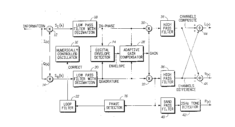
FIG. 1 illustrates an implementation of a "C-QUAM" stereo
receiver system 10 having a base band processor in accordance
30 with the present invention. The base band processor includes an
adaptive gain compensator 28, a multiplier 30, a multiplier 32, a
high pass filter 34, and a high pass filter 36. In addition to the
components of the base band processor, "C-QUAM" stereo receiver
system 10 also has a multiplier 12, a multiplier 14, a numerically
3 5 controlled oscillator 16, a first low pass filter with decimation
18, a second low pass filter with decimation 20, a loop filter 22, a
(6)
~0~739
(7)
digital envelope detector 24, a phase detector 26, a band pass
filter 40, a 25Hz tone detector 42, a first adder 44, and a second
adder 48. In the implementation described herein, loop filter 22,
phase detector 26, and numerically c,ontrolled oscillator 16 are
5 used to digitally correct the phase error component of the
modulated information signal.
A digital, modulated information signal labeled "Information"
is provided to the receiver system 10. The Information signal is
typically an analog signal which has been translated to lower
10 frequency, converted by an analog to digital converter (not shown)
to a digital signal, and has been transmitted by a "C-QUAM"
transmitter (not shown) to receiver system 10.
The Information signal is provided to a first input of both
multiplier 12 and multiplier 14. A cosine value of a phase
15 corrected intermediate frequency (IF) signal is labeled "I(k)" and is
provided to a second input of multiplier 12. Similarly, a sine value
of the phase corrected intermediate frequency signal is labeled
"Q(k)" and is provided to a second input of multiplier 14.
An output of multiplier 12 is labeled Sl(k) and provides an in-
20 phase component of the modulated information signal as an input tothe low pass filter with decimation 18. Low pass filter 18 filters
and decimates the Sl(k) signal to provide an output signal labeled
"In-phase." The In-phase signal is provided as a first input to each
of digital envelope detector 24, adaptive gain compensator 28, and
2 5 multiplier 30.
An output of multiplier 14 is labeled SQ(k) and provides a
quadrature component of the modulated information signal as an
input to the low pass filter with decimation 20. Low pass filter
20 filters and decimates the SQ(k) signal to provide an output
30 labeled "Quadrature." The Quadrature signal is provided as a second
input of digital envelope detector 24, a second input of adaptive
gain compensator 28, and a first input of multiplier 32.
Digital envelope detector 24 provides a signal labeled
"Envelope." The Envelope signal is provided as a third input to
35 adaptive gain compensator 28. An output of adaptive gain
compensator 28 is labeled "Gain" and provides a second input to
(7)
7 ~ 9
(8)
each of multiplier 30 and multiplier 32. An output of multiplier 30
is provided to high pass filter 34. High pass filter 34 filters the
output of multiplier 30 to provide a signal labeled "Channels
Composite." The Channels Composite signal is provided as a first
input to both adder 44 and adder 48.
An output of multiplier 32 is provided to high pass filter 36.
High pass filter 36 filters the output of multiplier 32 to provide a
signal labeled "Channels Difference." The Channels difference
signal is subsequently provided to a second input of both adder 44
1 0 and adder 48.
An output of adder 44 is a signal labeled "L(n)" and an output of
adder 48 is a signal labeled "R(n)." Both the L(n) and R(n) signals
are provided to an external user of "C-QUAM" receiver system 10.
The output of multiplier 32 is also provided to band pass filter
1 5 40 and phase detector 26. An output of band pass filter 40
provides an input to 25 Hz tone detector 42. An output of 25 Hz
tone detector 24 provides an output labeled "P(n)" to an external
user of "C-QUAM" receiver system 10.
An output of phase detector 26 is provided to an input of loop
filter 22. Loop filter 22 provides a signal labeled "Correct" to an
input of numerically controlled oscillator 16. Numerically
controlled oscillator 16 subsequently provides the l(k) signal
which reflects an adjusted phase error to the second input of
multiplier 12 and the Q(k) signal which also reflects the adjusted
phase error to the second input of multiplier 14.
During operation, multipliers 12 and 14 serve to digitally
frequency translate and demodulate the Information signal.
Similarly, adaptive gain compensator 28 and multipliers 30 and 32
collectively function to provide the Gain signal containing
3 0 information necessary to form the left and right channels of an
audio signal from the in-phase and quadrature components of the
Information signal. Additionally, loop filter 22 and numerically
controlled oscillator 16 collectively estimate and correct a phase
error of the Information signal.
3 5 A software program may be executed within a digital signal
processor (not shown) to provide a fully digital implementation of
(8)
20~7~9
"C-QUAM" digital signal receiver in accordance with the present
invention. In the example described herein, stereo receiver system
10 may be implemented using a digital signal processor such as a
Motorola DSP56001. Other digital signal processors currently
5 available may also be used to implement the stereo receiver
system 10, however.
During operation, a modulated digital signal labeled
"Information" is provided to the first input of both multiplier 12
and multiplier 14. The Information signal is typically
10 characterized by the following equation:
(1) Information = [C+L(k) +R(k)] cos(w--k + g(k) + fe(k)).
In equation (1), C is a constant value equal to a carrier magnitude
15 of the Information signal, L(k) indicates the magnitude of a left
audio channel signal at a predetermined dimensionless time index
(k), and R(k) indicates the magnitude of a right audio channel signal
at a same predetermined time index (k). An angular center
frequency of the Information signal is equal to wc and an angular
2 0 sampling frequency of the Information signal by the external
analog to digital converter (not shown) previously discussed is
equal to ws. The value (k) is also provided to indicate the time
index. A quadrature information signal is reflected in equation (1 )
by the term g(k), and a phase error information component is
25 represented by the fe term. The quadrature information term g (k)
is expressed in the following form:
~L(k) - R(k) + .05sin(f 2~k)l
(2) g(k) = tan -1 l C + L(k) + R(k) J'
30 where the term (.05sin(f 21lk)) is a 25 Hz pilot tone used as a
reference signal by any conventional AM stereo receiver.
During transmission, a phase angle of an analog signal is
altered by surrounding conditions. For example, atmospheric
(9)
2~9~7~
(1 o)
conditions and receiver equipment lirnitations may modify the
phase angle of the transmitted, digital signal. Any phase angle
modifications must be approximated and corrected befure the
signal is output to a user of the receiver, or the signal will sound
5 distorted. Therefore, to enable the receiver to provide a quality
audio sound, modifications to the phase angle of the analog signal
must be detected and corrected before being provided to the user.
Multipliers 12 and 14 demodulate the Information signal to
respectively provide the in-phase sampled output signal labeled
10 "Sl(k)" and the quadrature sampled output signal labeled "SQ(k)." To
provide the Sl(k) signal, the Information signal is multiplied with a
predetermined first output signal labeled "I(k)" provided by
numerically controlled oscillator 16. The l(k) signal typically has
the form of:
1 5
(3) I(k) = cos(w k + fe(k)) .
The fe(k) term of equation (2) provides a phase error correction
value necessary to enable receiver system 10 to provide a quality
2 0 audio signal. Therefore, when multiplier 12 multiplies the
Information signal and the Itk) signal, the result is the Sl(k) signal
in the form of:
(4) Sl(k) = [(C+L(k) +R(k)) cos(wc k + g(k) + fe(k))] x [cos(w--k +
25 fe(k))],
which simpllfies to equation (5):
(5) Sl(k) = 2 [(C+L(k) +R(k)) cos[(g(k) + (fe - fe)]] + D(k),
where D(k) is a double frequency term. Additionally, the term k is
dropped in the fe and fe terms as each varies very slowly with
ti me .
(1 o)
(11 ) 2~ ~ 73~
Similarly, to provide the SQ(k) signal, the Information signal
is multiplied with a predetermined second output signal labeled
"Q(k)" provided by numerically controlled oscillator 16. The Q(k)
signal typically has the form of:
( 6) Q(k) = -sin(wc k + fe(k))
Therefore, when multiplier 14 multiplies the Information signal to
the Q(k) signal, the result is the SQ(k) signal in the form of:
1 0
(7) SQ(k) = [(C+L(k) +R(k)) cos~ k + g(k) + fe(k))] x [-sin(wc k +
fe(k))] ~
which simplifies to equation (8):
1 5
(8) SQ(k) = 2 [C(1+L(k) +R(k))] sin [(g(k) + (fe - fe)] + D(k),
where D(k) is again the double frequency term.
The Sl(k) and SQ(k) signals are respectively a demodulated in-
20 phase component and a demodulated quadrature component of the
Information signal. The low pass filters with decimation 18 and
20 both remove the double frequency terms, D(k), and lower the
sampling frequency of each of the Sl(k) and SQ(k) signals.
In this example, low pass filters with decimation 18 and 20
2 5 filter the double frequency term, D(k) and subsequently decimate
the Sl(k) and SQ(k) input signals by four, respectively. During
decimation, the Sl(k) and SQ(k) input signals are sampled at a
frequency which is a fraction of the input frequency of the signals.
For example, when the low pass filter with decimation 18
30 decimates by four, the Sl(k) signal is sampled at a frequency which
is one-fourth the frequency at which the Sl(k) signal is input to the
low pass filter with decimation 18. Therefore, a signal output
from each one of the low pass fiiters with decimation 18 and 20
(1 1)
7 3 ~
(1 2)
has a sampling frequency which is one-fourth of the frequency at
which the signal was input.
Low pass filter with decimation 18 provides the In-phase
signal to an input of each of digital envelope detector 24, adaptive
5 gain compensator 28, and multiplier 30. The In-phase signal has
the form:
(9) In-phase = 2 [(C-~L(n) +R(n)) cos(g(n) + (fe - fê))]
10 As shown in equation (9), low pass filter with decimation 18
removes the double frequency term D(k) from the Sl(k) signal. As
well, the decimation is reflected by a new time index, n, where n is
equal to (4--). Therefore, the Sl(k) signal given by equation (5) is
provided without the double frequency term D(k) and at a lower
15 sampling frequency. Low pass filter with decimation 18 may be
implemented by using a standard low pass digital filter with a
decimation process. The standard low pass digital filter with the
decimation process may be digitally implemented as a series of
conventional software instructions which is executed in the data
2 0 processor.
Similarly, low pass filter with decimation 20 provides the
Quadrature signal to both an input of digital envelope detector 24,
adaptive gain compensator 28, and multiplier 32. The Quadrature
signal has the form:
(10) Quadrature = 2 [(C+L(n) +R(n)) sin (g(n) + (fe - fe))]
As shown in equation (10), low pass filter with decimation 20
removes the double frequency term D(k) from the SQ(k) signal. As
30 well, the decimation is also reflected by the new time index, n,
where n is equal to (4--). Therefore, the SQ(k) signal given by
equation (8) is provided without the double frequency term D(k) and
at a lower sampling frequency. Like low pass filter 18, low pass
( 1 2)
2~9~7~9
(1 3)
filter with decimation 20 may be implemented by using a standard
low pass digital filter with a decimation process. Similarly, the
standard low pass digital filter with the decimation process may
be digitally implemented as a series of software instructions
5 which is executed in the data processor.
The In-phase and the Quadrature signals respectively provide
demodulated decimated in-phase and quadrature signals to the
remaining portion of receiver system 10. In the example described
herein, the In-phase and Quadrature signals are obtained digitally.
10 However, both signals might also be the sampled inputs of an
analog receiver (not shown). Both signals are input to digital
envelope detector 24 to provide the Envelope signal. The value of
the Envelope signal is determined from both the In-phase and the
Quadrature signals and provides a signal indicating the value of the
15 envelope of the Information signal. The Envelope signal has the
form:
(1 1 ) Envelope = ~ In-phase2(n)+ Quadrature2(n).
2 0 By using commonly known trigonometric identities, equation (1 1 )
may be simplified to provide the "Envelope" signal with the form:
(12) Envelope = 2 (C + L(n) + R(n)).
2 5 Digital envelope detector 24 uses a conventional multiplier
circuit (not shown) to compute the square values of the In-phase
and the Quadrature signals, a conventional adder circuit (not
shown) to add the squares of the In-phase and the Quadrature
signals, and a conventional circuit to compute the square root of
the composite of the squares of the In-phase and the Quadrature
signals. The multiplier circuit, the adder, and the circuit to
compute the square root are typically resident in the data
processor, and therefore, a software program to enable the data
processor to execute the operation performed by the digital
envelope detector 24 may be easily implemented.
( 1 3 )
209~739
( 1 4 )
The output of the digital envelope detector 24, the Envelope
signal, is provided to adaptive gain compensator 28. Adaptive gain
compensator 28 provides a gain factor which may be used to form a
left and a right channel of audio information from each of the In-
5 phase and Quadrature signals . The gain factor is provided byadaptive gain compensator 28 as the Gain signal.
The Gain signal is provided using an iterative process which
approximates and corrects a value of the Gain signal. The iterative
process is given in the following equation:
1 0
(13) Gainj+1 = Gainj + D[s Envelope - Gainj- In-phase].
In equation (13), the subscript i refers to a point in time at
which the approximation is being generated. Therefore, when the
15 subscript i+1 is given, an approximation at a subsequent point in
time is executing. The "D" is a first scaling factor which is chosen
to correct a difference between an actual and theoretical value of
the Gainj signal. Additionally, the s is a second scaling factor
which is used to modify the Envelope signal to equal the product of
20 the Gain and In-phase signals. Both the D and s values are chosen
in accordance with characteristics of receiver system 10 and will
vary for each system used.
During operation, the iterative process of equation (13) is
complete when Gainj+1 equals Gainj. To achieve this equality, it is
25 necessary for the "s Envelope - Gainj- In-phase" portion of
equation (13) to converge to zero. By arithmetically manipulating
the aforesaid portion of equation (13), the following relationship
may be extracted:
30 (14) Gainj In-phase = In phaseP
Equation (14) may be further simplified by combining equation (9)
with equation (12) to provide the following relationship. Phase
error is considered to be negligible.
( 1 4)
20~739
(1 5)
(15) In-phase = Envelope ~ cos g (n)
When the relationship given in equation (15) is applied to equation
(14), the value of the Gain signal is expressed as:
(16) Gainj= s ( )
Therefore, by using multiplier 30 to multiply the In-phase and the
Gain signals, a resulting product has the form:
1 0
(17) Gainj In-phase= s Envelope
( 1 8 ) G ai n j I n-phase = 2 (C+L+R)
The in-phase component of the Information signal is
reflected in the composite of the left and right channels of the
audio signal. Next, to obtain quadrature information from the
Information signal input to receiver system 10, a signal containing
the difference between the left and right channels must be
2 0 extracted from the Information signal. As in the in-phase
component of the Information signal, equation (10) is combined
with equation (12) to provide the following relationship:
(19) Quadrature = Envelope sin g (n).
Subsequently, multiplier 32 is used to multiply the Quadrature
signal and the Gain signal with the following result:
(20) Quadrature Gain = (Envelope sin g (n))(COs g (n))
(21 ) Quadrature Gain = s Envelope tan g (n).
As was previously stated in equation (2):
(15)
~9~73~
( 1 6)
L-R+P
( 2 2 ) tan 9 (n) = C+L+R
as was shown in equation (12), Envelope is equal to "2 (C+L+R)".
Therefo re,
L-R+P
(23) tan g (n) = 2Envelope
By combining equations (20) and (23), the product of the Quadrature
and Gain signals is equal to:
1 0
(24) Quadrature Gain = 2 ( L-R).
Each of the outputs of multipliers 30 and 32 is then high pass
filtered by high pass filters 34 and 36, respectively. High pass
15 filter 34 removes the constant value "C" from the product provided
by multiplier 30 to provide the Channels Composite signal of the
form:
(25) Channels Composite = L + R.
Similarly, high pass filter 36 removes the pilot tone "P(n)"
from the product output by multiplier 32 to provide the Channels
Difference signal. The Channels Difference signal has the form:
25 (26) Channels Difference= L- R.
The Channels Difference signal is negated and added to the
Channels Composite signal by adder 48 to produce a signal labeled
"R(n)." The R(n) signal provides right stereophonic information to a
3 0 user of receiver 10. Similarly, the Channels Difference signal
provides a second input to adder 44. Adder 44 adds the Channels
Difference and Channels Composite signals to provide a signal
(1 6)
209~7~9
( 1 7)
labeled "L(n)." The L(n) signal provicles left stereophonic
information to the user of receiver system 10.
By allowing only frequencies within a predetermined range of
frequencies to be output from band pass filter 40, the in-phase and
5 quadrature information signals and the phase error information are
not output from band pass filter 40. Rather, band pass filter 40
allows only the pilot frequency signal P(n) to pass through and be
output to the 25 Hz Tone Detector 42. Upon receipt of the P(n)
signal, the 25 Hz Tone Detector 42 provides a signal to indicate
10 that the pilot signal P(n) is present.
The phase error which occurs during transmission of the
Information signal is typically due to time delay, atmospheric
conditions, or receiver non-linearities. Both atmospheric
conditions and receiver non-linearities generally modify the phase
15 of the Information signal with a low frequency signal. Therefore,
phase detector 26 is basically a low pass filter which detects the
phase error inherent in the Information signal. Detector 26 is a
conventional low pass digital filter circuit which is digitally
implemented as a software program executed by the data
20 processor. Phase detector 26 is connected to loop filter 22 to
provide an output which includes only phase error information. The
filtering operation executed by phase detector 26 may be executed
using standard and conventional logic circuitry controlled by a
predetermined software program. A sample of a predetermined
2 5 software program written for use with a Motorola DSP56001 is
provided in Appendix 1.
When the loop filter 22 receives the output of multiplier 32,
the Correct signal is provided. The Correct signal is then provided
to numerically controlled oscillator 16. Numerically controlled
30 oscillator 16 then uses the Correct signal to generate the l(k) and
Q(k) signals.
Operations executed by numerically controlled oscillator 16
may be executed using standard and conventional logic circuitry or
by a predetermined software program in a data processor. A next
3 5 sample of the Information signal is demodulated with the
multipliers 12 and 14, and the phase error of the signal is
( 1 7)
20.~073~
(1 8)
approximated by numerically controlled oscillator 16. Therefore,
the phase angle of the signal is approximated and iteratively
converged by calculating the sine and cosine of the phase error.
FIG. 2 provides a flow chart of the series of steps executed by
5 the base band processor described herein to separate the left and
right audio channels of the Information signal. As was previously
described, the base band processor includes adaptive gain
compensator 28, multipliers 30 and 32, and high pass filters 34
and 36. Each of the functions required to perform the operations
10 executed by the base band processor described herein may be
performed with a software program. An example of one software
implementation is provided in Appendix 1. The software program in
Appendix I is executed by a Motorola DSP56001 digital signal
processor.
15Referring to FIG. 2, the steps necessary to separate the
Information signal into a left and a right channel may be
summarized as follows:
1. Obtain In-phase and Quadrature signals;
2. Compute Envelope value (equations (11) and (12));
3. Concurrently, multiply the Envelope signal by s and
multiply the In-phase signal by the Gain signal;
4. Subtract the product of the In-phase and Gain signals
from the product of the Envelope signal and s
5. Compute the Gainj+1 value using the formula given in
equation (1 3)
6. Concurrently, multiply the In-phase signal by Gainj+
and multiply the Quadrature signal by Gainj+1; and
7. High pass filter each of the products formed in step 6 to
provide both a composite signal having both the left and
right channels of audio information, and a difference
signal which also has both the left and right channels of
audio information.
35In the base band processor described herein, the left and right
channels are balanced with respect to each other. The Gain signal
(18)
20~0739
(1 9)
is concurrently provided to both multiplier 30 and multiplier 32.
Additionally, high pass filter 34 and 36 are implemented
identically such that they are matched and provide outputs at the
same rate. Similarly, adders 44 and 48 receive and arithmetically
manipulate a Channels Composite signal and a Channels Difference
signal concurrently such that the left audio information
corresponds to the right audio information. Because the operations
performed on each of the in-phase and quadrature components of
the Information signal are executed concurrently and
symmetrically, the left and right audio signals are "naturally"
balanced by the design of the system and do not require
compensating circuitry as was previously required in analog
implementations of C-QUAM receivers. Therefore, the complexity
of the base band processor described herein is greatly simplified
by the symmetrical nature of both the circuit and method used to
produce the left and right channels of audio information.
Additionally, the implementation of the AM receiver described
herein may be fully implemented using digital, rather than analog
logic. Therefore, noise associated with the discrete components of
an analog solution is not present. However, an analog demodulator
may also be used to provide the In-phase and Quadrature signals to
the inputs of the base band processors. Additionally, by using a
digital solution, the left and right channels of audio information
may be generated exactly rather than approximated as was
performed by analog components. Subsequently, a clearer, more
accurate reproduction of the audio sound is generated. Receiver
system 10 is also able to provide better quality audio sound
because the adaptive gain compensator is multiplied by both the
In-phase signal and the Quadrature signal after each has been
filtered and decimated to a lower frequency. As was previously
stated, the gain factor may be generated more accurately at lower
frequencies. Additionally, the low pass filtering serves to remove
a substantial portion of the noise generated during transmission of
the Information signal.
Furthermore, each of the steps and functions performed by the
digital receiver described herein may be implemented as a
(1 9)
20~9~739
(20)
software program. The software program would be subsequently
executed by a digital data processor. In particular, current
hardware implementations of digital signal processor devices
would adequately support the requirements of the digital "C-QUAM"
stereo receiver system 10 described herein.
It should be well understood that the digital "C-QUAM" stereo
receiver system described herein provides a wide variety of sound
enhancements. The implementation of the invention described
herein is provided by way of example only, however, and many other
implementations may exist for executing the function described
herein. For example, a plurality of software programs may be
provided to respectively perform the arithmetic functions executed
by each of the components of the receiver system 10. The plurality
of software programs are provided by the user of the receiver
system 10 and may be executed on any one of a plurality of digital
data processors. Additionally, the plurality of software programs
may be slightly modified to enable each one of the plurality of
digital data processors to perform the arithmetic functions
described above.
Each one of the components of the receiver system 10 may be
digitally implemented in a software program and executed in a
digital data processing system. A series of software instructions
would enable a typical digital signal processor to execute each of
the functions performed by multiplier 12, multiplier 14,
numerically controlled oscillator 16, low pass filter with
decimation 18, low pass filter with decimation 20, loop filter 22,
digital envelope detector 24, phase detector 26, adaptive gain
compensator 28, multiplier 30, multiplier 32, high pass filter 34,
high pass filter 36, adder 44, adder 48, band pass filter 40, and 25
Hz tone detector 42. For example, a single general purpose
multiplier in the digital signal processor may be used to perform
each of the functions executed by multiplier 12, multiplier 14,
multiplier 30, and multiplier 32.
Additionally, the form and content of the software program is
dependent on the user of the receiver system 10. The circuitry
used to perform the mathematical computations required by the
(20)
2090739
(2 1 )
software programs is implemented in a conventional form.
Conventional adders, multipliers, and dividers are typically used to
implement a software program to perforrn the functions described
herein .
While there have been described herein the principles of the
invention, it is to be clearly understood to those skilled in the art
that this description is made only by way of example and not as a
limitation to the scope of the invention. Accordingly, it is
intended, by the appended claims, to cover all modifications of the
invention which fall within the true spirit and scope of the
invention .
(2 1 )
20~73~
(22)
Appendix I
This subroutine performs the function of determining tan (fe-
fe) with a low pass filter in a Motorola DSP56001 digital signal
5 processor. For further information on the software instructions
implemented within the subroutine, refer to "DSP56000/DSP56001
Digital Signal Processor User's Manual, (DSP56000UM/AD)"
published by Motorola Inc. in 1989. In FIG. 1, this subroutine is
represented by phase detector 26. The input to the detector is the
1 0 output of the quadrature channel manipulator 38. It is called qstar
in this program. The pointers r6 and r7 respectively point to the
previous input and output data of the phase detector 26. The terms
1 pfr6, 1 pfr7, 1 pfcddr, and nomod are labels which indicate offset
values determined by a user of the DSP56001. The pointer r2
1 5 points to coefficients of the low pass filter. The modulo addresses
m2, m6, and m7 are determined accordingly.
org p:$100
move y:qstar, y1 ;move the output of
;the quadrature
;channel manipulator
;38 into register yl
move x:1 pfr6,r6 ;move the location of
2 5 ;the previous input
;data into pointer r6
move x:1 pfr7,r7 ;move the location of
;the previous output
;data into pointer r7
move x:1pfcddr,r2 ;move the location of
;the filter
;coefficient into
;pointer r2
move #1,m6 ;set up modulo
3 5 ;addresses
move m6,m7
(22)
(23) 2~7~
move #nomod, m2
rnove x:(r2)+,xO ;move the first filter
;coefficient into
;register xO
The following five instructions perform the filter,
accumulating the result in a register a and incrementing through
the coefficients, the old input data and the old output data. On the
last instruction, the latest input data is stored to a memory
10 location for use when the next sample is filtered. The output of
the filter is moved to register x1, and will then become the input
to the loop filter 22.
mpy xO,yl,a x:(r2)+,xO y:(r6)+,yO
mac xO,yO,a x:(r2)+,xO y:(r6), yO
mac xO,yO,a x:(r2)+,xO y:(r7)+,yO
mac xO,yO,a x:(r2)+,xO y:(r7),yO
mac xO,yO,a yl,y:(r6)
20 The final line of code moves the filter to register x1 and moves the
new output into the new output memory for use on the next sample
to be filtered.
move a,xl a,y:(r7)
(23)
2~73~
(24)
Appendix ll
This subroutine performs the function of providing the Gain
signal as disclosed in the specification in a Motorola DSP56001
5 digital signal processor. For further information on the software
instructions implemented within the subroutine, refer to
"DSP56000/DSP56001 Digital Signal Processor User's Manual,
(DSP56000UM/AD)" published by Motorola Inc. in 1989. In FIG. 1,
this subroutine is represented by both digital envelope detector 24
1 0 and adaptive gain compensator 28. A first input to envelope
detector 24 is the In-Phase signal which is called "iin" in this
program . A second input to envelope detector 24 is the Quadrature
signal which is called "qin" in this program.
1 5 org p:start
move x:ichannel,xO ;move the output of
;the low pass filter
;with decimation 18
;into register xO-this
2 0 ;is the In-phase
;signal as shown in
;FIG.1
move y:qchannel,yO ;move the output of
;the low pass filter
2 5 ;with decimation 20
; i nto reg ister yO-th is
;is the Quadrature
;signal as shown in
;FIG.1
move xO,x:iin ;store the value
;transferred by the
;In-phase signal in a
;storage location
;specified by x:iin
3 5 move yO,y:qin ;store the value
;transferred by the
(24)
209~73~
(25)
;Quadrature signal in
;a storage location
;specified by y:qin
mpy xO,xO,a xO,b ;Square the value
;transmitted via the
;In-phase signal and
;store the results in
;register a
macr yO,yO,a b,x1 ;Square the value
;transmitted via the
;Quadrature signal
;and add the squared
;value to the square
;of the In-phase
;signal already
;stored in register a-
;Store the sum in
;register a
move a,xO ;move the contents of
2 O ;register a into
;register xO
jmp <sqrt ;Jump to a subroutine
;which executes a
;square root
;function-the result
;of the square root
;function is the
;output of digital
;envelope detector
;24, the Envelope
;signal which is
;stored in register b
rep # 3 ;arithmetically shift
;the Envelope signal
3 5 ;three times to the;right to effectively
(25)
2 ~ 3 ~
(26)
;multiply th0
;Envelope signal by
;s- in the example
;described herein,
;s= .125.
asr b
move x:iin,xO ;move the value
;transferred by the
;In-phase signal to
;register xO
move y:gainfactor,y1 ;move a previously
;stored value of the
;Gain signal to
;register y1
mpy xO,y1,a ;Multiply the value
;transferred by the
;In-phase signal and
;the value
;transferred by the
;previously stored
;Gain signal and store
;the results in
; reg iste r a
sub a,b #>bgainm1,yO ;Subtract the
2 5 ;contents of register
;a from the contents
;of register b
;(Envelope s- In-
;phase-Gain j)
3 0 c I r a b,x1 ;clear register a for
;subsequent
;operations
move y1,a ;move the previously
;stored value of the
;Gain signal to
;register a
(26)
(27) 20~73~
m
macr x1,yO,a y:qin, yO Gaini+1 = ~,x,
i =O
;where x =Gainj+
;D[s Envelope
;Gain;-ln-phase]
;store the result in
;register a
move a,y1 ;Move the contents of
;register a (the
;Gainj+1) into
;register y1
mpy y1,yO,a a,y:gainfactor ;Multiply the value
;transferred via the
;Quadrature signal
;times the value of
1 5 ;the Gainj+1 signal,
;store the result in
;the register a
mpy y1,xO,b ;Multiply the value
;transferred via the
2 O ;In-phase signal
;times the value of
;the Gainj+1 signal,
;store the result in
;the register b
Subsequently, the contents of each of registers a and b are filtered
by high pass filter 34 and high pass filter 36, respectively.
(27)