Note: Descriptions are shown in the official language in which they were submitted.
2 ~ 3 7
89R097
IMPROVED EFFICIENCY DRIVER SYSTEM FOR PIE70ELECTRICS
James R. Hall
BACKGROUND OF THE INVENTION
Field of the Invention
This invention relates to electric drives for piezoelectric actuators
and more particularly to energy transfer between two piezoelectric
elements for increasing -the system ef~iciency of operation.
Description of the Related Art
Piezoelectric actuators and other high-capacitive devices require
high Yoltage drive. Drivlng them linearly with a conventional ampliFier
requires a large reactive current and results in correspondingly high
losses.
.. - :~,~ . ,, ~,.
. . :: :: .. . :: :
; ~
,
:-.. . -~.
~:
2 ~
Improvements have been made such as in Skipper patent num~er
4,628,275 to provide efficient power amplifiers for such devices. ~owever
the capacitive energy stored -in the actuator which is recaptured and used
to reduce the energy requirements of the actuator systems is subject to
the same losses during recovery as during the charge portion of the cycle.
SUMMARY OF THE INVENTION
This invention uses the capacitive energy stored in an activated
piezoelectric actuator which is to be deactivated to activate a
piezoelectric actuator which has little or no capacitive energy stored in
it.
The energy of one capacitive actuator is switched through an inductor
to a second actuator. The timing of the switching and the rate of transfer
- of energy are tailored to the functional needs of the actuator. Energy is
added to the system from a voltage source to make up for the losses in the
system and for the work done by the actuators.
,:
' .
1 7
OBJECTS OF THE INVENTION
It is one object of the invention to increase the efficiency of a
piezoelectric actuator system by transferring capacitive energy from one
actuator to another directly rather than discharging an actuator and
sending the energy back to a power source energy store.
Other objects, advantages and novel features of the present invention
will become apparent from the following detailed description of the
invention when considered in conjunction with the accompanying drawings
BRIEF DESCRIPTION OF THE DRAWINGS
1~ Figure l is a schematic view of the related art having a piezoelectric
-actuator which returns its capacitive energy to the energy source.
Figure 2 is a schematic view of one embodiment of the invention where the
capacitive energy stored in one piezoelectric actuator is used to activate
a second piezoelectric actuator.
Figure 3 is a schematic of a second embodiment of the inventi~n.
' .- . - - ' ' ' , .: ' `
, ~ , : j ' ,, : ~ : ,
'
- ' L , ,: ~
2~3 ~ 7
Figure 4 is a schematic of a portion of the invention in which a non
linear inductor is used.
Figure 5 is a graph of the voltage and current of the circuit of figure 4.
Figure 6 is a schematic of a portion of the invention in which a linear
inductor is used.
Figure 7 is a graph of the voltage and current of the circuit of figure 6.
DETAILED DESCRIPTION OF THE PREFERRED EMBODIMENT
Electrodeformable materials such as piezoelectric material provide
sonversion of electrical energy to mechanical work. This work appears as
- electrical loads that are mainly capacitive in nature with the work energy
being a small resistive component to the driver circuit. Charge must be
transferred to the capacitor to produce motion resulting in work if the
motion drives a mechanical load. If there is no mechanical load the energy
from the charge transfer is stored in the capacitor to be recovered later
when the charge is removed and the motion is reversed. With no mechanical
load the losses are limited to the circuit losses plus the internal losses
of the piezoelectric element. The electrical equivalent is shown in the
figures wherein pie~oelectric actuators 5 and 6 have a capacitor
indicating that piezoelectric devices act as capacitors, a series variable
, : ~. ...... : , ,..... . . -
.-
. ' ' ~ ~ -
: :
2 ~ 7
resistance representing the mechanical load and a resistor to show a
minimum value of resistance representing internal losses.
Typically piezoelectric materials can transfer 2-13 % of the
electrical energy they receive to useful work. This results in a large
ratio of drive energy compared to wor~ energy, and therefore could result
in a very low efficiency system if great care is not exercised in the
energy transfer and recovery circuitry in the driver to recapture energy
stored in the material as capacitive energy.
As in all high efficiency capacitor charging systems the circuit must
have minimum resistive losses in the controlling switching elements and
the inductor.
A typical LC charging system is shown in Figure 1. Energy is
transferred from the energy source 1 to the actuator 5 through inductor 4
by moving switch Swl to position 1. Current magnitude and the resulting
charge rate is controlled by alternating Swl from position 1 to 3 so that
average applied voltage and average current produce the charge rate.
- -- When the desired charge voltage (or current time product) is achieved
the switch may be moved to position 2 to hold the charge.
To remove the charge, Swl can be moved to position ~ so that energy
recovery may be achieved by returning the stored energy to the source.
There are many variations of recovery circuits, all of which have to
overcome the problem where both the charge and recovery portions of the
cycle are subject to the loss of energy during transfer in the inductor
and switching elements.
,, : . . .
'
:.
2~9~7
A typical system consisting of an energy source, switch elements, and
transfer inductor might achieve efficiencies of 0.9 to 0.95 if carefully
designed. Assuming a piezoelectric transfer efficiency of .05 the overall
system efficiency nS may be calculated.
nS = Energy Load / (Energy loss ~ Energy Load)
Where Energy Load = EL = 0-05 Ec
Ec = Charge Energy
Energy loss = El = (l - 0.92) Ec
The energy loss occurs on both charge and recovery therefore
0-05 Ec
- - nS=
[2 (l - 0.092) Ec ~ 0-05 ~c]
= 0.05
(0 l6 + 0.05)
= 0.24
Thus with 92 percent e~ficient circuitry and a lossless piezo element
only 2~X system efficiency is realized because of the large circulating
energy which is subject to circuit losses.
.
~: ,' ' ~ ~ ':'
.
17
In some actuators layers of piezoelectric material are stacked and
each layer driven by a different wavP form such that mechanical summing of
the layers results in a desired actuator movement. For a complete
explanation see Rockwell International Corporation's copending patent
application serial number 07/743,069 filed August 9, l99l which is a
continuation of serial number 07J488,548 filed March 5 , l990 for an
Electrical Drive for a Segmented Transducer which is hereby rnade a part
hereof and incorporated herein by reference.
In some actuator designs such as those found in U.S. Patent
4,928,030, for a Piezoelectric Actuator issued May 22, l990, U.S. Patent
5,0l7,820 for a Piezoelectric Rotary Union System issued May 2l, l99l and
U.S. Patent 5,068,566 for an Electric Traction Motor issued November 26,
l99l all of which are made a part hereof and incorporated herein by
reference, multiple pairs of actuators operate in smooth walking motion to
alternately contact and move objects. These actuators are particularly
receptive of the present invention because one actuator is being
- discharged while an adjacent actuator is being charged.
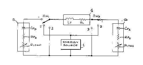
Figure 2 shows that a significant system efficiency improvement can
be achieved by having two or more actuators which work alternately so that
the energy from one actuator is transferred directly to a second actuator.
As an example, assume that in the initial condition piezoelectric
actuator 5 is fully charged and piezoelectric actuator 6 has zero charge.
Switch 2 is in position l connecting piezoelectric actuator 6 to the
transfer inductor 4 and switch l is alternated between position l and 3,
by a controller, to transfer energy ~rom piezoelectric actuator 5 through
- :
, , ~
.
1 7
transfer inductor 4 to piezoelectric actuator 6 at the desired rate. In
this configuration the energy transfer will allow the charges to equalize
the vol~age on the piezoelectric actuators.
If switch 2 remains in position l until the current rises in
sinusoidal manner to the peak value determined by
_V
~ ( L/C )
and decays to zero, all charge will transfer from piezoelectric actuator 5
to piezoelectric actuator 6. Switch 2 can then be moved to position 3 for
isolating the charge on piezoelectric actuator 6.
During this process piezoelectric actuator 5 moves to its rest state
and piezoelectric actuator 6 moves to its stressed state.
Since the transfer of energy results in some loss, and since
additional energy loss occurs if piezoelectric actuator 6 is doing some
work, the energy in the system would be depleted to zero after several
transfers. However additional energy may be added to the system by
utilizing position 2 of the control switches l and 2, to introduce
additional energy from the source to make up for the losses.
If the sinusoidal transfer of charge current is not desirable because
of the required motion of the piezoelectric actuators, an alternate
operating mode where both switch l and switch 2 alternately transfer
between positions l and 3, the energy will flow piece wise from
piezoelectric aetuator 5 to piezoelectric actuator 6 by moving from the
electrostatic field of the piezoelectric actuators to the electromagnetic
field of the inductor and then to the electrostatic field of the second
piezoelectric actuator.
-
,
.
2~ 17
The limitation of using identically reversed wave forms to charge anddischarge the piezoelectric actuator pairs has eliminated transferring all
of the recovered energy to the source and then to the other piezoelectric
actuator, and the transfer losses are approximately halved. The net
efficiency for the system is approximately
.S Ec
[(1 - 0.092)EC + 0~05EC]
= 0.05
(0.08+0.05)
= 0.38
which is l.6 times the previous value.
Many LC energy transfer configurations using both linear and non
linear inductive elements may be implemented, but the efficiency of the
system always improves if the circulating energy moves between the
piezoelectric actuators with the fewest intermediate energy storage
elements and switches.
In the embodiment shown in figure 3, current from the energy source l
charges the inductor 4, which is ~hen transferred to one or the other
piezoelectric actuators 5 or 6, until the desired charge (and charge rate
is achieved) then the energy is transferred from piezoelectric actuator 5
to piezoelectric actuator 6 and back as required, with occasional
supplements from the energy source to make up losses and supply the energy
required by the work being done.
"
".. ~
,
; ., : .,
.
; .
- :
~ : '
.
lo
Many inductor circuits may be used in the above design. By ~Jay of
example figures 4 and 6 show two inductor circuits which may be used
An example of a non linear inductor (saturable reactor) transfer
circuit which produces an oscillatory wave form which is a pseudo square
wave is shown in figure 4, where piezoelectric actuators 5 and 6 are of
equal capacitance and the transfer inductor 4 is a saturable inductor with
values of L unsaturated and L saturated.
As the chart in figure 5 shows, piezoelectric actuator 5 is charged
and piezoelectric actuator 6 is at zero charge when Switch l is closed to
start the cycle at time zero. Current slowly rises in inductor 4 until
current saturation, when the volt second rating of the inductor is
reached. When the inductor saturates the cirsuit impedance rapidly drops
to a new value determined by L saturation. A sinusoidal current then flows
from piezoelectric actuator 5 through the conductor to piezoelectric
actuator 6 during the period ~rom T to -r . When the current drops to
zero the inductor unsaturates During the period from T to T
- piezoeléctric actuator 6 is charged7 piezoelectric actuator 5 has zero
charge and the low frequency transfer of charge from piezoelectric
actuator 6 to piezoelectric actuator 5 begins. The current magnitude is
deter~ined by L unsaturated as is the oscillatory frequency. As the
current slowly increases the I saturation value is reached in V x t time,
the inductor saturates in the other end of the B H loop and rapid
retransf~r of the charge occurs. ~he transfer time is controlled by L
saturation and the hold time by L unsaturation. The rest of the hold time
can be extended by opening switch l when the current is at zero. The
' ~ '
~,
. ,
combination of the saturable inductor with a switch for controlled hold
times results in less stress on the switch compared to using a fixed
inductor and switch since the large value of L unsaturated reduces di/dt
after the switch closure and allows time to complete the switch closure
function before large current values flow. The fixed inductor circuit in
figure 6 does not have the slowly changing current (representing the
longer time constant of t=~L unsaturated x Cpz) between charge transfer
pulses as shown in figure 7.
Many other combinations of multiple switches, inductors, or nonlinear
inductors may be used to produce variations charging current wave forms to
produce desired motions of the piezoelectric actuators, but if the devices
are operated with complementary motions so that the energy stored in each
half of the system can be transferred to the other half without returning
it to the source the transfer losses can be minimized and higher system
efficiency will be achieved.
The controller for operating the switches can have sensors on the
- piezoelectric elements and on the inductor to tell the controller what the
state of the element or inductor is as well as providing information as to
the position of the act~ator.
Obviously, many modifications and variations of the present invention
are possible in light of the above teachings. It is therefore to be
understood that, within the scope of the appended claims, the invention
may be practiced otherwise than as specifically described.
,
, "