Note: Descriptions are shown in the official language in which they were submitted.
RPqgl4~ 03-LO-63$0
GEN 9254 PATENT
MULTIPARAMETER ECM AND
CONTFt~.7L TI~EFtE
~~ c~c~roull~ of t 'invention
This invention generally relates to electronically
controlled motors and to systems, such as heating, ventilat-
ing and/or air conditioning systems having motors therein
operating according to predetermined parameters which are
selected to correspond to the system in which the motor is
installed.
while conventional brush-commutated DC motors may
have advantageous characteristics, including convenience of
changing operation speeds, there may be disadvantages such
as brush wear, electrical loss, noise and radio frequency
interference caused by sparking between the brushes and the
segmented commutator, and overall material cost of the motor.
These disadvanfeages may limit the applicability of such
brash-commutated DC ~not~rs ia~ c~any fxeld~, including the
refrigeration, heating; ventilati.rig and/or air conditioning
~H~AC) fields. EleGtzonically commu'tated motors, such as
brushless DC motors arid permanent magnet motors with elec-
tronic come~autation, have now been developed and generally
are believed t~ have the advantageous characteristics of
brush-cQmmutated DC motors without many of the disadvantages
thereof while also having other important advantages. Such
electronically cammutat~d motors are disclosed in the lDavid
~9. Erdman U.S. Patent Nos. 4,015.12 and 4,459,519, for
instance. Such electronically commutated motors may be
advantageously employed, for instance, in HvAC systems which
employ variable sg~eed motors.
Present motors have a variety of features and
operational and system parameters which must be adjusted to
optimize performance by providing a proper speed-torque
1
;; 'y.: w ,y ~
RMH19~ 03-LO-630
GEN 9 2 5 4 P~.TENT
characteristic for a particular application. Further, in '
many system applications, the starting torque and/or speed-
torque characteristics of the motors must be predictable and
repeatable. In addition, it is desirable that motors be
operable at the highest reasonably achievable efficiency
consistent with mass production techniques. Known present
variable speed motors~cannot easily achieve this advantage
because it has traditionally been impractical or too costly
to minimize the variable effect on motor characteristics
caused by manufacturing tolerances of the internal components
of the motor. Present concepts and arrangements for adjust-
ing a motor for different applications require circuit
changes such as multiple variable resistors in the electronic
control for the motor or permanent software changes in an
electronic control microprocessor. Both of the aforemen-
tioned arrangements are disadvantageous because they require
a unique model to be built for calibratine~ a system which
cannot be easily changed and can be quite expensive.
In the specific case of I~T~,C systems. such systems
may include a variety of backup heat ratings~ operate in a
variety of modes, have variable capacities and be installed
in a ~rariety of environments. Both the speed and torque of
an electric motor. which affect air flow through the system,
are affected by the aforementioned variables. Interfacing a
control microprocessor with the necessary information to
make these changes often requises complex assemblies. creates
possible shock hazards and/or limits the number of available
variations.
~,mrnarw of the Inver~~ion
An object of the. present invention is the provision
of an improved central heating, air conditioning and
2
RI~9B148 03-LO-6380
GEI~i 9254 PATENT'
2fl~~~~~
ventilating system permitting defining operating parameters
based on the environment of the system.
Another object of the invention is to provide a
system which permits optimum airflow for ma~cimum comfort
andlor efficiency for varied system environments.
Still another object is to provide a system which
permits interfacing defined parameters or characteristics of
a motor with a memory associated with a control for an
electronically commutated motor.
Still another object is to provide a system w~xich
permits interfacing a system control signal, such as a
temperature signal from a thermostat, with a motor control
for the motor.
it is yet another object of this invention to
provide a system which permits calibrating a motor contro l
to actual characteristics or operating parameters of a motor
while driving a known load.
Yet ar~ottaer object is to provide a system which
permits calibrate:ng the motor to a known,load.
A still further abject is to provide a system
which permits calibrating a moto r control to .motor
characteristics under a no load condition.
Yet other objects are to control a motor by a
microprocessor via an application specific integrated
circuit.
Another object is to prAVide such a system which
permits sensang the position of a rotating assembly of the
motor far controlling torque and speed of the motor.
A still further object is to provide a system
which permits~sen~ing back electromotive force in a winding
of the motor for sensing the position of the rotating
assembly.
Yet another object is to provide such a system
which permits selecting varied frequencies of pulse width
modulation for controlling the motor.
3
ttr~t~leti 03-hO-6380
GhN 9 2 5 ~ 1?ATEPIT
2~~~~~~'
Still another object is to provide such a system
which permits limiting current in the windings of the motor
to a reference level.
Another object is to provide such a system in a
manner which is economically feasible and commercially
practical.
Briefly described, the system of the present
invention drives a component of a heating ventilating,
and/or air conditioning (IivAC) system ~in response to a
system control signal provided by a central means, such as a
temperature signal provided by a thermostat. The system
includes a motor, a memory, means for generating control
signals and an instruction memory. The orator has a
stationary assembly and a rotatable assembly in magnetic
coupling relation to tho stationary assembly, the rotatable
assembly in driving relation to the componena. The motor
drives the component in resgonse to a control signal. The
memory stores parameters representative of the system. The
means for gsneratinc~ control signals controls motor speed or
2Q torque and includes a microprocessor responsive to one or
more stored parameters ahd to the system control signal.
The -instruction memory stores instructions controlling the
operation of the microprocessor.
Alternatively, the system of the present invention
drives a component iaa response to a system control signal.
The system comprises a motor, a memory and means for generat-
ing control signals. The motor has a stationary assembly
and a rotatable assembly in magnetic coupling relation to
the stationary assembly, said rotatable assembly in driving
3Q relation to the component. The motor drives the component
in response to a control signal. 'The memory stores calibrat-
ing parameters representative of operation of the motor
driving a predetermined load. The means for generating
4
RM13148 03-LO-6380
GEN 9254 PATENT
~~~i~~~~
control signals controls motor speed ar torque in response
to the calibrating parameters and to the system control
signal.
Alternatively, the invention may comprise various
other systems and methods.
Other objects and features will be in part
apparent and in part pointed out hereinafter.
$.~.~.pf ~~S~riPtion of. thw'
Figure 1 is a block diagram of one preferred
embodiment of an EC~I drive system of the invention and
including an application specific integrated circuit (ASIC)..
Figure 2 i~ a partial schematic diagram of one
preferred embodiment of a parameter control signal interface
and various parameter control signals of the invention
1S generated by the interface.
Figure 3 is a partial schematic diagram of one
preferred embodiment of the system control signal interface.
Figure 4 is a schematic diagram of. one preferred
embodiment of portions of the block diagram of Figure 1.
Figure 5 is a block diagram of one preferred
embodiment of an application specific IC (ASIC) of the
invention.
Figure 6 is a block diagram of one preferred
embodiment o~ the current blanking circuit of the ASIC shown
in Fig~xre 5,
Figure ? is a block diagram of one preferred
embodiment of the reference current circuit of the ASIC
shown in Figure S.
Figure 8 zs a schematic diagram of one preferred
embodiment of the pseudo - randomrpulse width modulation
frequency generator of the ASIC show~a ire Figure 5.
S
a
RIe1B148 03--lL0-6380
PATFNT
GEid 9254
Figure 9 is a schematic diagram of one preferred
embodiment of the back FMF voltage sensing network shown in
Figure 4.
Figure 10 is a schematic diagram of one preferred
embodiment of the xera crossing detector, employing
synchronous sampling, of the ASIC shown in Figure 5.
Figures 12a to l:~d are a timing diagram
illustrating one preferred embodiment of a preferred
commutation strategy relating to zero crossings and
blanking.
Figures 12a to ltd are a timing diagram
illustrating one preferred embodiment of commutation
and sequencing of the invention.
Figures 13A-13~ illustrate one preferred
embodiment of a schematic diagram of the commutation logic
circuit and back ~lF decoder of the ASIC of Figure 5.
Figure 14 i.s a sclaer~atic diagram of one preferred
embodiment of an undervoltage detector of the ASIC of Figure
5.
Ffgure 15 is a schematic diagram of one preferred
embodiment of the level shifters of the ASIC of Figure 5.
Figure i~ is _ a schemat~.c diagram of one preferred
embodiment of the pseudo random FWWt~I frequency generator and
clock management of the ASIC of Figure 5.
Figure 17 is a sch~:matic diagram of one preferred
embodiment of the I'wM frequency selector of the ASIC of
Figure 5.
Figure 1~ is a schematic diagram of one preferred
embodiment of.the position sensing back E1~F multiplexes of
the ASIC of Figure 5.
Figure 19 is a schematic diagram of one preferred
embodiment of the drive watcta dog circuit of the ASIC of
Figure 5.
5
RMH148 U:i-LU-(~abU
GEN 9254 PATENT
2U~~'~~~
Figure 20 is a schematic diagram of one preferred
embodiment of the current regulation circuit of the ASIC of
Figure 5.
Figure 21 is a schematic diagram of one preferred
embodiment of the current blanking circuit of the ASIC of
Figure 5.
Figure 22 is a schematic diagram of one preferred
embodiment of the current reference generating circuit of
the ASIC of Figure 5.
Figure 23 is a schematic diagram of one preferred
embodiment of the zero cross~.ng counters, the commutation
and blanking counters and the underspeed detector circuit of
the ASIC of Figure 5.
Figure 24 is a schematic diagram oø one preferred
embodiment of the microcontroller ~ratch dog circuit of the
ASIC of Figure 5.
Figure 25 is a layout diagram of figures 25A-25C.
Figure 25A-25C are a schematic diagram of one
preferred embodiment of the zero crossing detector, flyback
voltage detector and adaptive blanltinc~ circuit of the ASIC
of Figure 5. .
Figure 26 is a schematic diagram of one preferred
embodiment of the gate drives to the pov~er switches of
Figure 1.
Corresponding reference characters indicate
correspo~ading parts throughout the drawrings.
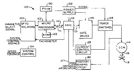
Refaxring to Figure l, a system 100, one preferred
embodiment of the present invention, wtaich is part of an
indoor unit (not shown):of a heating. venti3.ating or air
conditioning (I~tAC? system for mo~i~g air, is illustrated.
System 100 includes a microprocessor 102 for receiving via
7
..
RI~R148 03-LO-630
GEN 9254 PATENT
optical isolators 103 a temperature signal and/or other
system control signals generated by a system control 104. A
read only memory (ROM) 106 having software is used to '
control the operation of the microprocessor 102. ROM 106
S may be incorporated with microprocessor 102 embodied as a
microcontroller. Microprocessor 102 provides a set of motor
control signals (M.C.S.) via lane 110 to an application
specific integrated circuit (ASIC) 17.2. or universal electron-
ically commutated motor integrated circuit (tJECM IC, not
shown) for electronically controlling a plurality of gate
drives 130 (see Figure 26). The ASIC 17.2 provides informa-
tion to microprocessor 102 via line 7.7.1. The ASIC 112. pro-
vides level shifted gate drive signals via line 131. which'
have been shifted from 5 volts to 10 volts in; order to
provide enough voltage to swatch a plurality of power
switches 124 (see figure 26) . The power switches 124 are
use to control a motor such as a variable speed induction
motor, a switched reluctance motor or an electronically
commutated motor (ECPI) 114. For exampleo speed or torque of
the motor may be controlled by controlling the power
delivered to th.e load in order to control an air flow rate
of an N~AC which includes the syste~a 100. Electronically
commutated motor (ECM.) 114 lass a rotatable assembly (not
shown), or rotor, mechanically connected via a shaft 116 to
a particular device to be driven, such as a blower, a
compressor or a draft inducer (not shown) or a fan 118.
In addition. a programmable, non-volatile (PNV)
memory 120 may be provided for storing various system
parameters, as will be described below in greater detail,
which parameters are used by the microprocessor 102 to
determine operation of motor 114. PNV memory 120 may be an
electrically erasable programmable read only memory (EEPROM).
System 100 also includes a power supply 122 which provides
power to operate the microprocessor 102 and A~IC 112 which
8
RMB148 03-LO-6300
GEiV 9 2 5 4 PATEPlT
drives the associated power switches 124. Power supply 122
also provides high voltage d.c. (H.V.D.C.) to the power
switches 124 for driving the windings o~ the electronically
commutated motor 114.
Motor 114 may include means for sensing the
position of its rotatable assembly such as a position
sensing circuit 125 for sensing a back electromotive force
(BEMF) and which provides a zero crossing detector signal
via line 127 to which ASIC 112 is responsive. A BEMF
sensing circuit 126A (see Figure 4) includes a sensing
network and comparators. Microprocessor 102 may also
include an internal analog-to-digital converter (not shown)
fox converting incoming analog signals into digital signals
for further psocessi~g.
The ASIC 112 also responds to a current control
circuit 129 for detecting overcurrent conditions in the
windings of motor 114. The system of the invention includes
two overcurrent detecting circuits 129A (see Figure 4), both
of which provide signals to the ASIC 112, to provide redun-
dant overcurrent information. A current blanking scheme in
ASIC lI2 differ~ntzates between an actual overcuxrent signal
and a false one caused by noise in the circuit. In the
event of an overcurrent condition. the ASIC 112 removes the
power applied tn the motor 114 by turning off the gate drive
signals. Current control circuit 129 also includes a
current regulator 1298 (see Figure 4) providing a regulation
signal (IREG) t~ AS1C 11.2. The current control circuit 129
as well as the internal overcurrent protection of the ASIC
will be described in greater detail below.
The microprocessor 102 may be associated with
programmable nonvolatile (PtJV) memory 120 storing parameters
representative of the system such as time constants which
are a function of the thermal mass of the structure being
heated and/or cooled by the indoor unit of the HvAC.
9
RMH14$ ~l3-LO-630
GFN X254 PATEfiiT
~fl~~~~~
Alternatively. PNV memory 120 may store parameters represen-
tative of the system characteristics. The microprocessor
102 may by connected via optoisolators 103 to a keypad or
dip switches (not shown) responsive to operator input for
providing a parameter select signal by selecting at least
one of the stored parameters. The microprocessor lOZ
generates motor control signals (M.C.S.) via line 110 based
on the parameters stored in memory 120 and in response to
the parameter select signals thereby c~ntrolling the system
100. Alternatively, it is contemplated that the PN'J memory
120 may include a parameter stored therein which is repre-
sentative of the rotor magneti~atian level of the rotatable
assembly. As a result, the motor control signals generated
by the microprocessor 102 would be a function of the stored
parameter in addition to the control signal parameters.
The system 100 may also be responsive to a mode
signal provided to the microprocessor 102 via optoisolators
103 as a system control signal. For example, the mode
signal may determine whether system 100 operates in a
thermostat m~de os in a variable speed mode: A Pv~t mode
signal indicates variable sped or torque operation of the
motor ~rith the i3uty cycle of tae mode signal corresponding
to the desired motor speed or tongue. In this configura-
tion, microprocessor 102 detecting system control signals
via optoisolators 103 would constitute means for detecting
as a system control signal a mode signal having a particular
form and means for selecting parameters for use by tha
control signal generating means in response to the detected
mode signal.
Figure 1 illustrates system 100 according to the
invention for conditioning air in a space by moving the air
or by heating or cooling the air to change its temperature.
System control 10~. such as a conventional thermostat,
constitutes means for generating a system control signal
RMH148 03-LO-fi380
GEN 9254 FATENT
such as a temperature signal corresponding to the tempera-
tune of the air space as it .rises and falls. This system .
control signal is provided to microprocessor lOZ via optical
isolators 103.
For eRample. the EEPROM may have one or more of
the following parameters stared therein: speed or air flow
rate fox various operating modes such as a heating mode and
a cooling mode; speed or air flow rates for different system
capacities such as tons of cooling and 3cilowatts of heating;
parameters defining turn-on' and turn-off time delays;
parameters defining motor speed or torque changes over time;
parameters defining the relatianship between motor. torque
and air flow; parameters defining the relationship between
motor speed and ais flow: and parameters defining direction
of rotation; and wherein the control signals generated by
the microprocessor are a function of at least one of the
stored parameters. Alternatively, tlxe EEFROM may include a
' parameter stored therein which is representative of a
difference betc~een the actual power input into the system
and the escpect~d nominal pourer so than the control signals
generated by the microprocessor 102 are a functian of the
difference.
As shown in Figure 1, system 100 constitutes
variable speed motor 119 which has a rotatable assembly, or
rotor, in driving relation to the component such as fan
I18. System 100 is responsive to the system control signal
and has programmable nonvolatile (Pt~VV? memory i20 which
stores parameters representative of system 100. The motor
control signal provided by microprocessor 102 to ASZC 112
via line 110 is responsive to at least one of the stored
parameters plus the parameters selected in response to the
parameter select signal and to the system control signal.
System 100 provides the M.C.S. to ECM 1I4 to control its
speed or torque, ROM lOfi stores instructions which control
11
RME148 03-LO-6380
GEN 9254 PATENT
the operation of microprocessor 102. The microprocessor 102
constitutes means responsive to the system control signals
provided via optical isolators 103 by system control 109.
The microprocessor 102 receives the system control signals,
such as the temperature signal and monitors it to generate -
the motor control signal provided via line 110 as a function
of the system control~signal and the parameter select signal
as well as any stored parameters.
Various time constants may be stored in.PNV memory
120 which correspond to various parameters of various
environments. Microprocessor 102 may be programmed at the
factory or during field installation to select time constants
corresponding to the environments within which the indoor
unit including system 100 is being installed. The stared
parameters may correspond to a constant CFM calibration,
i.e., representative of a calibrated operation of the ECM
114 driving a predetermined, known Ioad so that micropro-
cessor 102 would be accurately responsive to the stared
parameters.
As part of the process of manufacture. system 100
is operated with a known calibratibn load. with a predeter-
mined current versus speed characteristic. This load, for
example, could be an ECM driving a blower wheel with a known
restriction to tie flow of air. It could also be an arti-
2~ ficial lead which electronically simulates the loading
characteristics and waveforms present at the terminals of
motor 114. The system 100 is calibrated by running it on
this calibration load and commanding it to deliver, in
sequence; one or more current levels to the load. For
example, it may first be commanded to provide the full or
maximum current level and then a relatively low current
level. In each case, the actual current delivered by the
system 100 is measured either directly or indirectly by
measuring the speed achieved on tka~ calibration load. Due
a
12
FtMB148 03-LU-6380
GEN 9254 PATE~7T
~Q~'~~.~~
to circuit tolerances within the particular system I00, the
actual current values may be somewhat different from the car-
rest or nominal values. This actual information generates a
current offset factor and a multiplier factor compensating
for the inaccuracies within the system I00. The compensation
factors are stored permanently in the PNV memory 120. In
this manner, tkie system 100 is calibrated to coe~pensate for
the tolerance variations of its internal components.
Alternatively. the parameters may be represents-
tive of a calibrated operation of ECM 114 driving no load so
that the microprocessor 102 is accurately responsive to such
stored parameters. In the case of ECM 1.14, an alternate
simplified method of calibration may be used. The system
100 is run at no load and the no load speed is measured. No
I5 load speed is a very good indicator of rotor magnetization
Ievel which is the predominant cause of torque variations .
Storing this information al.on~g with the previously obtained
control calibration information in an EEPRCM used as PNV
memory 120 allows subsequent compensation for most of such
tolerance variations. PJo load motor tests are much less
time consuming than load tests and do not require_a dyna-
mometer. As such. they are r~aatin~ly performed anywhere.
The built-in microprocessor lOZ in the control can by itself
measure the no load speed and store the data in the PNV
memory 120, requiring minimal external equipment.
Alternatively, the parameters stored in Pt~V memory
I20 may be representative of an operation of a particular
motor I19 in combination with a particular system 100 to
provide a represen~:ative operation of particular motor II4.
For example, the stored parameters may represent the differ-
ence between the act~.ial tordue generated by a particular
motor 114 and the nominal values thereby representing the
combined inaccuracies of the particular motor I14 in .
.. combination with the microprocessor 102. In a number of
13
RMH14~ 03-LO-6380
GIN 9 2 5 4 1'~T~HT
applications, the system 100 and the motor 114 are physically
attached together and distributed as a single unit. In such ,
cases, the system 100 would be programmed with not only its
own inaccuracies but also those of the motor 114 to which it
is attached.
Generallyo the system 100 without motor 114 is
first calibrated by one of the methods described above. The
calibrated system is then connected to the motor 114. T'he , ,
system and motor combination are then calibrated,. for
example, by running them an a loading/measuring device such
as a dynamometer. Certain torque levels) are commanded of
the system 100 and motor 114 and the resulting actual
torques are measured. The difference between the actual
torques and the correct or nominal values represents the
combined inaccuracy of the system and the motor. This
information is stored in the F1~V meanory 1~0 to enable the
microprocessor 102 to produce near-nomimal torque in the
actual operation by compensating for the tolerance
inaccuracies of both motor 114 and system 100.
This correlation bet~reen actual and nominal values
may be eztended beyend Bmproveanent of system and moto r
combinat~.on accuracy to calibration of variations in the
tasget system. ~ typical application for variable speed
motors is driving blower wheels in gas furnaces or indoor
fan coil units of central heat~.ng and air conditioning
systems. The key performance parameter is blower air flow
which depends on motor speed-torque characteristics,
restriction lave? (static pressure) in an installation, and
physical characteristics of the blower wheel such as blade
pitch, etc. Methods have been previously devised to gener-
ally compensate for the static pressure variations, making
the air flow somewhat independent of a~nstallatzon. However.
to achieve the best air flow accuracy. unit to unit varia-
tions due to blower wheel characterista,cs need to be
14
uM~s~a us-i,o-b3~u
GEN 9254 PATENT
calibrated out. This can be accomplished in the following
manner. A calibrated system and motor combination is
installed in the particular blower wheel of a furnace or fan
coil unit. The inlet and outlet openings of the unit are
kept at a predetermined level, including completely open,
thus, ensuring a known restriction level. Operation of the
motor 114 with a certain system control signal provided to
the control should then result in a predictable nominal
blower speed or power. The actual blower speed or power is
measured and ate deviation from nominal represents the
inaccuracy of tk~e blower wheel. This information is stored
in the PI~1V' memory 120 so that microprocessor 102 can
compensate in actual operation.
rn one preferred embodiment, memory 120 comprises
an EEPROM having one or more of the following parameters ,
stored therein: speed or air flow rate for various operating
modes such as a heating mode and a cooling mode; speed or
air flow rates for different system capacities such as tons
of cooling or kilowatts of heating;, parameters defining
turn-on and turn-off time delays; and parameters defining
direction of rotation. Each pafameter may also differ
depending on the mode of operation. For example, the
following modes may be used: heat pump, backup heat.
emergency heating, dehumidifier, fan only, or other modes.
As a result, the motor control signals generated by micro-
processor 102 and provided via line 110 would be a function
of at least one or more of the stored parameters.
As noted above, it is also contemplated that the
memory 120 may include a correction factor (such as a
current offset or a multiplier) for tolerance inaccuracies
of the any one or more portions of the system. For example,
the memory 120 may include a parameter stored therein which
is representative of the difference between the actual
current being delivered to the motor 114 and the expected
RMB148 03-LO-6380
GEN 9254 PATENT
nominal current. As a result, the motor control signals
provided by microprocessor 102 via line 110 would be a .
function of this stored correction factor parameter.
The parameters stored in the memory may also be
representative of the difference between the actual speed of
the component being driven by the motor or the actual power
input (watts} into the motor 114 and the expected nominal
speed or input power sp that the motor control signal
generated by the microprocessor 102 would be a function of
this stored parameter.
In accordance with one feature of the invention,
Figure 2 illustrates means for providing parameter select
signals to the microprocessor 102. The ECM 114 of the
system 100 may be configured for driving fans, such as fan
118. far a variety of I~iVAC system having different heat pump
cagacities and backup heat ratings. Further, the fans may
operate in a variety of modes such as cooling. dehumidifica-
tion, fan only, heating and the like. The ECM 114 can
provide optimum air flow in etch case for maximum comfort
and/or efficienby. Tn accordance With the present invention,
the microprocessor 1Q2 controls the ECM 114 in r.esponsa to
selected parameters corresponding to a set of operating
parameters selected at a.nstallation in the field including
fan speedy CompresS~r speed, heat output and the like.
Selecting the parameters is referred to as the field
selection process.
In a preferred embodiment, the system 100 directly
interfaces the microprocessor 102 with parameter select
signals by diode duplexing. As shown in figure 2, a 24 volt
alternating current (24vAC? supply voltage 200,is applied to
a positively biased diode 202 which rectifies the AC voltage
and provides a positive half wave output signal 204. A
negatively biased diode 206 similarly rectifies the 24vAC
signal and provides a negative half wave output signal 208.
16
RMB148 03-LO-6380
GEN 9 2 54 FATEI3T
The rectified half wave signals are selectively ,
connected to the microprocessor 102 through optical isolators
103 as parameter select signals as either the full cycle
24VAG supply voltage 200, the positive half wave output
signal 204, the negative half wave output signal 208 or no
signal is interfaced with the microprocessor 102. Thus,
field selection consists of connecting each of four of the
optical isolators 103 to one of four field select lines 210,
212, 214. 216 to provide one of the above four signals as an
input to microprocessor 102 via the optical isolators 103.
This is eduivalent to having four selection switches, each
with four positions.
The pt~ memory 120 stores at a particular address
a set of operating parameters for the system 100 correspond
ing to a defined air flow rate. The microprocessor 102
reads the particular address in tine PIE memory 120 corre-
sponding to the air flow rate sele~:ted by the parameter
select signals. The operating parameters stored at the
particular address are used by the microprocessor 102 to
control fan speed i.n r~spons~ to compressor speed and
desired 11e8t ~LbtpLit. DI3.CroprOC~SSOr 1~2, thLtS, -CalCUlates
appropriate air flow rates for given configurations of
system i00 from the parameter select signals.
Figure 3 shows a preferred embodiment of circuit
for providing the system control signals to microprocessor
102 according to the present invention. The microprocessor
102 controls the ECM 114 zn response to a number of system
control signals provided by system control 104 such as a
temperature signal provided by a thermostat. ~?ther system
control signals include a blower activating command, an
electric beet command, fizst and second stage compressor
commands, a reversing valve command and a humidistat low .
humidity signal. The microprocessor 102 defines an
operating mode for the ECM 114 in response to the system
17
~MHl4s o3-~o-63aoa
GEN 9254 PATENT
control signal. The ASIC 112 executes system control
commands. In one embodiment, the ECM I14 can respond to six
24 volt AC signals. Six system interface lines (not shown)
may be connected directly to a low voltage terminal board
S (aot shown) of the indoor unit. A variation of the "diode
duplexing°' concept used in field selection is implemented
with the ECM 114 for providing the system control signals to
the microprocessor 102.
A number of diodes, such as diodes 301 and 303 are
configured in bipolar diode pairs, such as pair 304, as shown
iia Figure 3. and a low voltage alternating current (AC)
supply voltage is selectively applied to the diodes.301 and
303. Each bipolar diode pair 304 grovides a composite
output signal froe~ node 305 to the optical isolators 103,
1~ the outgut of. which is directly presented to microprocessor
102. The composite output signal is a half wave signal only
when either diode 301 or diode 303 of the pair 304 receives
the AC supply voltage and is a full wave signal when both
diodes 301 and 303 of tlxe pair 304 receive the AC supply
voltage.
An operator may selectively apply the AC reference
voltage by mechanically opening or closing switches 307 and
309, such as in a thermostat, connected in series with
diodes 301 and 303, respectively. Alternatively. switches
307, 309 may be electronically controlled by system control
104. Table 1 shows the composite output signal which would
be provided to the microprocessor for different configura-
tions of switches 30'~ and 309.
TA~L~1
3 0 ~ ~ ~9.~. COMPOS'~~'~
Open Open No signal
Open Closed Negative Half-wave
Closed Open Positive Half-wave
Closed Closed Full Cycle
18
,; ;~ . ' ,. ;, r .. , ;
..:
~Jd-LU-6380
H (~'A1i 1 ~4 ti
GIN 9254
~ 0 ~ ~ ~ ~ ~ PAx~NT
Resistors 311 and 313 may be placed in series with
diodes 301 and 303, respectively, to limit power dissipation
by limiting current in diodes 301 and 303.
Figure 4 shows a schematic of portions of the
block diagram of Figure 1. Microprocessor 102 receives via
optical isolators 103 the system control and parameter select
signals. P~iV memory 120 stores various system parameters
which are used by microprocessor 102 to determine operation
of motor 114. In one preferred embodiment, power switches
124 are illustrated as an inverter bridge having a positive
bus 402 and a negative bus 404 supplied by a power supply
(not shown). Preferably. power switches 124 are activated
in pairs; one switch is closed for each winding of motor 114
to be energized. Power switches 406 and 40'7 correspond to
1S phase A. Power switches 408 and 409 correspond to phase ~.
Power switches 410 and 411 correspond to phase C. Power
switches 406--411 are driven by drivers 416-421 (see Figure
' 26), respectively, in response to drive signals provided by
ASIC 112. '~Yae excitation scheme for ECM 114 in~rolves
three-phase excitation with trapezoidal current excitation.
This may invblv~ the use of a three-stage full-bridge
inverter empl~ying six switches, such as power switches
406-411, and a flyback diode coupled in an anti-parallel
relationship with eadh switch of switches 406-411. In the
2S preferred embodiment, the anti-parallel diodes (not shown)
are included in switches 406-411. 3'wo switches are commanded
on during each motoring.interval, one prom the upper set of
switches 406, 406. 410 and one from the lower set of
switches 407, 409, 411. Current flows in only two of the
three motor phases during each excitation interval.
As illustrated in Figure 4, current control
circuit 129 includes overcurrent protection circuit 129A,
wtxich provides input signals to Tooth microprocessor 102 and
.. ASIC 112. and current regulator 129H providing an I~2EG
19
R~B14~ o3-.LO-630
GEN 9254 PATENT
signal to ASIC 112 in response to a current reference signal
(IREF) provided by ASIC 112 and a signal representing motor
phase current sensed in a resistive shunt 430 having
resistors Rshl and Rsh2 and providing outputs S0. S1 and
S S2. A back EMF sensing network 126A is part of position
sensing network 126 shown in Figure 1. The position sensing
and current control features are described below.
The ASIC 112 also provides voltage signals shifted
from 5 volts to 10 volts for driving the power switches
406-411. In the preferred embodiment illustrated, the
plurality of gate drives 416-421 drive the gates of the
power switches 406-411. Gate drives 416-421 condition the
signals provided vfa line 131 from ASIC 112 for optimal
operation of switches 406-411 by adjusting their switching
speed:
Phase currents of the ECM 114 can be sensed using
shunt resistors, current transfoxmers, Mall--effect current
sensors or ether sensors ar circuits. In the embodiment
illustrated, a shunt resistor 930 is placed on the negative
t7C bus 404 which supglies the power switches 406-411.
Referring to P'xgur~ 4, motor phase GUrrents are~sensed by
shunt resister 430 and only flaw through the resistor 430
when gower is being exchanged from the supply 402 to motor
114 and vice versa. The shunt 430 does not detect
circulating currents involving more than one motor phase.
Current in the windings of ECM 114 is compared to
a reference current signal (IREF) provided by ASIC 112. The
comparison results in a signal being input to ASIC 112 to
execute current regulation. In a preferred embodiment,
cycle-to-cycle current regulation is utilised by circuit
129B. Circuit 1298 provides a frequency determined by the
ASIC 112 during the current regulation cycle. Gate drives
416-421 energize two of the power switches 406-411, such as
switches 416 and 419, at the beginning of a Ptat~i cycle. This
RDi8148 03--LU-6380
GEN 9254 PATENT
2~~~~~
allows the current in the windings of motor 1'14 to increase
until reaching a threshold value set by the reference
current (IREF}. At this instant. one or both of the power
switches 416, 419, for example. are turned off causing motor
phase current to decay. Such switches remain off until the
beginning of the following PWM cycle, thus, completing one
regulation cycle. In~particular, ASIC 112 defines reference
current (IREF} which is input via line 429 to a comparator
432. The reference current is first converted from a
digital signal to an analog signal by a I7dA converter 435.
Comparator 432 compares the motor phase current sensed on
the shunt 430 via line 438 with the analog of the reference
current provided by line 429; the output of comparator 432
is logic level low when motor current~exceeds reference
current. Since motor torque is proportional to current, the
ASIC 112 controls the torque of the motor 114 in response to
the difference between the detected motor phase current and
the reference current.
Referring to the block diagram of the ASIC 12
illustrated in Figure 5. ASIC 112 controls the ECM 114 for
air moving applidations. ASIC 112, among other things,
senses the rotor position of the ECM 1I4, controls targue by
a motor phase current control and provides high level
voltage gate drive signals to control power switching
devices.
A master oscillator 502 (shown in more detail in
Figure 16} generates a clock signal which synchronizes fhe
timing of the op~e~ation of the various portions of the ASIC
112. ASIC 112 provides the clock signal to microprocessor
102. Further, an interface between the ASIC 112 and the
micropracessor 102 consists of several input/output data
lines shown in the black diagram of Figure 5. In the pre~-
ferred embodiment, three input lines form a serial interface y
., with ASIC 112. The interface provides seria l communication
21
.u....a'au VJ-LV-OJC9U
GEM 9254 PATENT
to the ASIC 112 of a current reference signal (IREF), a
direction of rotation command (FR), a blanking signal (IHLFC)
and a frequency selection signal (FS). Other signals
include an angle advance (ADV), a fastfslow commutation PWM
mode (F'M) and an overcurrent reset signal (RS). Register
504 stores data serially loaded in the microprocessor 102.
The ASIC 112 also provides data to the
microprocessor 102. The ASIC 112 resets microprocessor 102
when the clock signal (DATA-CLK) from the microprocessor 102
is absent for a predetermined interval of time. This is
accomplished by a microcontroller watchdog circuit 507
(shown in more detail in Fig~xre 24). The ASIC 112 provides
a reset signal to microprocessor 102 during system power
up. Also, ASIC 112 provides an ovescusrent latch output
which can be read by microprocessor 102 to determine whether
an overcurrerit condition exists. ASIC 13.2 also provides a
motor speed signal via line 554 to microprocessor 102.
ASIC 112 also includes varzous control circuits. '
A current reference circuit 510 (shown in more detail in
Figure 22) associated with the current reference signal
(IREF) from microprocessor 302. An overcurrent protection
limit 515 (shown in more detail in Figure 20 as a trip
latch) for detecting current conditions above a certain
limit and an undervoltage detector 513 (shown in more detail
2S in Figure 14) for detecting undervo3tage conditions may also
be a part of ASIC 112. In one preferred embodiment, an
undervoltage condition is defined as less than 8.5 volts in
a drive circuit having an input voltage supply of 10 volts
and a stable regulated output of 5 volts. In the event of
an undervoltage condition occurring for a predetermined
interval of time, ~:hp ASIC 112 resets the mie:roprocessor
302. Overcurrent protection circuit 129A and overcurrent
limit 515 provide~the drive circuit with redundant over-
current information. In the event of an overcurrent
22
RMH148 03-LO-6380
GFH 9254 PATRNT
condition, the ASIC 112 disables the motor 114. ASIC 112
also includes a level shifter circuit 518 (shown in more
detail in Figure 15) and a current blanking circuit 516
(shown in more detail in Figure 21) which allow micropro-
cessor 102 to differentiate an actual overcurrent signal
from a false one caused by noise in the circuit.
A PWi~i frequency selector 519 (shown in greater
detail in Figure 17) selects the freqraency at which FCM 114
is pulse width modulated. Selector 519 is responsive to the
frequency select (FS) signal provided via line 521 which
selects a pseudo-random PtNM frequency generator 524 (shown
in more detail in Figure 16) which provides a PWM signal via
line 529. In the preferred embodiment, four frequencies are
available: f8 = 18.6 kHz, f8e3 = 6.2 kHz. f10 = 4.6 kHz and
FR = pseudo random frequency. Selector 519 controls opera-
tion of the motor 114 by selecting a frequency of madulation
for the pulse width modulating of the voltage applied to the
motor 114. Relatively low P~VM frequencies (e. g., frequencies
less than 20 kHz) tendl to generate acoustic noise audible by
humans due to the natural resonant frequency of the various
components of system 100. Higher PPrIM frequencies, however,
cause greater heat dissipation problems in inverter power ',
switches 124. Excessive heating is especially a problem in
compact drives. The pseudo random PGIM frequency generator
524 reduces the effect of acoustic noise generated by the
FCM 114 allowing operation at lower PWM frequencies. The
ASIC 112 continuously and pseudo-randomly varies the PWi~t
frequency within a predefined range to reduce the annoying
effects of single tone acoustic noise. In one preferred °
embodiment of the invention. the Pwr1 frequency signal
produced by selector 513 via Line 529 is controlled by the
frequency select signal (FS) provided-by microprocessor 102
via line .521 and by a random sequence of numbers provided by
generator 524 vi.a line 526. As a result, the Pt~t~i frequency
23
RMB148 03-LO-6380
GEN 9254 PATENT
can be controlled from a frequency select signal provided by
microprocessor 102. Data stored in PNVM 120 determined
whether the PWM frequency is a fixed frequency or a variable
frequency from a pseudo random sequence of numbers from
generator 524.
Selector 519 may be a multiplexer circuit as
described below. The'function of the selector 519 can be
expressed by the following equation:
fRND a fi*(N/16) (N m 0, 15)
where fRND, is the PWM frequency, fi is the input frequency
to a binary rate multiplier (see Fig. 8), and N is binary
number generated in a pseudo random manner. The selector '
53.9 selects a PwM frequency from four available frquencies
(f8, f8.3, f10, fR). A two bit signal (FS) is used to
select frequency. The pseudo random frequency (fRND) is .
generated by a random number generator and the binary rate
multiplier.
Referring to Fagtare 5, roto r position sensing
circuit 530 includes a bacDc EMF' selector circuit 541 (shown
in more detail ~n Figure 18) for selecting the motor phase
voltage to be ~analy~ed according to the state of the power
switches 124. Selector 541 responds to the zero crossing
detector signal provided via lines 12°7 by the position .
sensing circuit 126 (Fig. 1) such as back EMF sensing
network 126A (Fig. 4). The digital signal representing
selected motor phase voltage is provided to a flyback
voltage detector 53S (see Figure 25C) which detects the
proximity of a zero crossing. Detector 535 enables a back
EMF sampling circuit. such es zero crossing signal detector
538 (see Figures 25A and 25H), to initiate the Tero crossing
detection.
ASIC 112 includes a current regulating circuit
(see Figure 20), a commutation logic circuit (including a ,
bidirectional state machine) and back EMF decoder 51? (see
24
At'lt7t~0 va-uv-~~uv
GEN 9254 PATENT
2~~~~~
Figure 13) which is a circuit for generating the commutation
logic for the system 100. The commutation logic consists of
a state machine which operates in response to the direction
of rotation command (FR). The states are incremented or
S decremented in response to a commutation signal (CMM) which
is generated by a commutation instant estimator circuit 550
(see Figure 25C) zesponsive to the zero crossings detected
by detector 538. The commutation signal (CMM) indicates the
time instant for commutation of a motor phase. The back EMF
decoder indicates ttae pair of the power switches 124 which
are active during each state. Thus. two of the three phases
of the motor 114 are aetive at any given time according to
the state of sensed back EMF voltage. In one preferred
embodiment, the circuit 517 has eight states and is deigned
in such a way that two of its eight possible states are
forbidden (0 and 7) . I~ these states are preseaat when the
system 100 is activated, it forces itself immediately to
W state one. Each state is decoded by the back emf decoder ,
circuit. Two of t3xe sip power swatclxes 124 are associated
with each state so that at any dime instant only two of
power switches 124 are commanded on causing the energization
of two of the three motor 114 phases.
The rotor position sensing circuit 530 of ASIC 112
also includes a drive watch dog or underspeed detector 532
(shown in more detail in Figure 1~). Detector 532 constantly
monitors the ECM 114 rotor speed within each commutation
interval and disables the motor I14 when rotor speed falls
below a thresh~ld speed. 5inee motor speed is compared to a
threshold during every commutation interval, detector 532
also functions as stall detection circuitry.
The commutation instant estimator circuit 550 and
an adaptive blanking circuit 553 (see Figures 23 arid 25C) ,
which is also a part of the rotor position sensing circuit
w 530, will be discussed in more detail below.
RME148 03-LO-6360
GEN 9254 PATENT
One aspect of ASIC 112 is shown in greater detail
in Figure 6. Figure 6 illustrates a block diagram of the
current blanking circuit 516 (shown in greater detail in
Figure 21). The diode recovery current, present after one
of the power switching devices 124 is commanded on, causes
erroneous current information in the current regulator '
comparator 432 in the~form of a current spike. The ampli-
tude of this current spike can be several times higher than
the current level to be regulated. Flanking ignores the
erroneous current information from current comparator 432
caused by the diode recovery current. A high to low
transition of the current comparator 432 output reflects the
presence of current spikes triggering a blanking time
interval block 601. The wadth of the interval is selectable
1S by input N via line 604. The generated blanking interval is
propagated through a gate G1 if its occurrence is within a
time interval, or window, of duration W as indicated by
reference character 60'1. The window 60? is initiated at the
beginning of the regulation cycle when the switches 124 are
turned on. A gate G2 modifies the information from current
comparator 432 by preventing the propagation of the low
state of comparator 432 when the blanking signal from the
blanking time interval block 601 and the window time interval
signal 607 are present. The high to low transition of the
output of gate G2 via line 610 during a window interval
represents a true overcurrent signal and terminates the PwM
current regulation cycle.
If the current regulate signal (low state) via
line 609 occurs after the window interval of 607, then the
signal is interpreted as a true current regulate signal and
no blanking interval is generated. The action taken by an
ASIC 112 current regulator in the presence of a current
regulate signal via line 610 is to immediately terminate the
PWM cycle.
26
GEC 9254 E'ATEP1T
The present invention includes blanking means
rather than using filters to reduce the effects of erroneous
information from the current comparatar 432. Turning on and
turning off events of power switches 124 cause current
spikes due to the nature of semiconductor devices. Conven-
tional techniques to reduce the effect of the current spikes
require the use of low pass filter arrangements. The
filtering of the current information from the shunt 430 is
usually done befare it is compared against the current
reference by comparator 432. The time constant associated
with a filter reduces the performance of the current
comparator circuit 129B, particularly at low current levels.
Without blanking, a pasitive current spike at
turn-on of switches 124 causes erroneous infarmatian about
the motor phase current which prematurely terminates the
current regulatian PWfI cycle, thus, causing a drug in phase
current and a drop in torque. Blanking ignores the
erroneous current information from current comgarator 432
caused by the diade reca~rery current. A negative current
spike at turn-off has no effect in this embodiment of the
present invention since by the time of its occurrence, the
PWT~ regulation cycle i,s already terminated.
Referring to Figure 7, one aspect of the ASZC 112
is shown in greater detail in block diagram form. The
reference current circuit 510 generates a digital signal
representing a reference current of constant frequency and
variably duty cycle generated by digital comparator 701 and
flip flop 704 having a clock signal via line 710. In one
preferred embodiment of the invention, digital comparator
701 may campr_ise ten exclusive i30R gates (see Figure 22).
One input signal to each XNOR gate is a bit from a ten-bit
binary number representative of a desired maximum current
magnitude. The binary number corresponds to a signal of a
particular duty cycle, of which the analog equivalent is
z7
Rl~lti 14 8 03-LO-63 80
GEN 9254 PATENT
compared to phase current. The other input signal to each
XNOR gate is one of ten signals o~ different frequencies. A ;
logic level high output szgnal from the XNOR gates indicates
that both input levels are the same. The outputs of each
XNOR gate are connected to a HAND gate. the output signal of
which is at a low level when the state of all individual
comparatars (i.e., each XNOR gate) is at logic level high
indicating the occurrence of a match. The output of the
multiple input NAND gate is connected to the reset input of
flip flop 704 via line 707. thus. causing flip flop 704 to
go to a low level until the next clock signal via line 710.
The output signal of flip flop 701 is of constant frequency,
as determined by the frequency o~ the clock signal via line
710, and of variable duty cycle, as determined by which
10-bit binary number is selected.
The PWNi current reference signal is passed through
a D/A convene r 435 functioning as a lour pass filter
' (outside the ASIC 112) and its output voltage is fed into
analog comparator 432 far comparison with the voltage
developed across shunt 430 (set Figure 4).
The variable duty cycle signal generated by
digital comparator 701 can also be used to synchronize new
data that has previously been loaded into ASIC 7.12 from
microprocessor 102.
Referring to Figure 8, pseudo random number
generator 524 (see Figure 16) of ASIC 11.2 is shown in
greater detail in block diagram form. Random number
generator 524 may consist of a 1S-bit closed loop shift
register shown as integrated circuit blocks IC6 and IC7.
The shift register is advanced. or clocked at an input
f requency fSI3IFT. Gates IC4 and ICS provide feedback and
initialization of the shift register 5241.
A fear-bit binary rate multiplier 5191 may be
commanded by 16 possible binary combinations of N. Four
23
RMB148 03-LO-6380
GEN 9254 ~ ~ ~ ~ ~ ~ PATENT
binary numbers (corresponding to 0 through 3) are forbidden.
Thus, ASIC 112 implements a mapping circuit in the form of
IC2 and IC3 to provide the following relationship:
S A ~ A' , B $ B' , C = C' and D ~ (C' '~ D' ) + D'
where A', 8', C' and D' are outputs of the shift register
circuit IC6 and IC7 and A, B, C and D are inputs to the
binary rate multiplier 5191.
The mapping prevents the PWM frequency from being
too low causing substantial loss in current which would
result in a loss in torque and possibly a loss of rotor
synchronism.
Referring to Figure 9, the system 100 includes
means ~or sensing the position of the rotatable assembly of
1S the motor 114 such as a back EMP' sensing network 126A. The
position sensing network 126A senses the back EMF to provide
a zero crossing detector signal (2CA, ZCB, ZCC~ to which ASIC
112 responds. The network 1Z6A senses rotor position as ~a
function of zero crossings ~f the difference between the back
EM!F voltage of windings of the motor 114 as compared to a
reference level Yn' developed by a resistive network function-
ing as a voltage divider. ASIA 112 generates power switching
control signals for power switches l24 in response to such
position sensing.
In one preferred embodiment, the ECM 114 rotor
position sensing network 126A is employed with a motor with
star conaxected windings and with 120 degree conduction
intervals. Two o~ the three motor windings are energized at
any given time developing torque. The third winding is used
for position sensing by observing the motor phase back EMF
Waves when current in the selected phase teas decayed to zero.
The back EMS' voltage waves are conditioned to a
signal level using a voltage divider network as shown in
Figure 9. Back EMF sensing network 126A conditions the motor
29
R~IB148 03-LO-6380
GEN 9254 PATENT
phase voltages va, vb, and vc to signals va' , vb' , and vc'
for phases A, H, and C, respectively. A conditioned signal
for the~motor neutral voltage (vn') is artificially generated
as a reference level as a function of the conditioned signals
of phases A, B, and C. zf a neutral voltage (vn) is avail-
able, its conditioned signal may be obtained in similar
fashion to the other motor ghases. Signals va', vb', and vc'
are compared against signal vn' by comparators CA, CB and CC,
respectively. Digital level high at the output of. the com-
parators indicates that a phase's back EhiF voltage magnitude
is less than the neutral voltage. Conversely, a low level
indicates that a phase's voltage magnitude is greater than
the neutral voltage. The digital representation of back EMF
voltages at the output of the comparators CA, CB or CC which
indicates the polarity of the back Efi2F voltages is shown in
Figure 9 as ZCA, ZCB, and ZCC for phase A. phase B. and phase
C, respectively. xn the absence of pulse width modulation in
the inverter power switches 124, the signals from the compara-
tors CA, CB and CC are square waves except for a short time
interval after each commutation. In presence of a PWM signal,
noise generated during switching events of the power switches
124 deteriorates the signal from comparators CA, CH and CG to
the eactent that it cannot be used without further processing.
If low pass filters are used to eliminate the noise effects
generated by the PVC action, however, the motor 114 high
speed performance deteriorates because the filter time
constant affect the angle at which commutation takes place.
Detecting the time instants of the zero crossing of
the back EP~° waves consists of sampling the back EMF voltage
waves during periods when the noise generated by turning on
and turning off events of the enabled power switches 124 is
at a minimum. Turning power switches l24 on or off generates
current spikes by the recovery of semiconductor switching
devices. The transient voltages generated by these spikes
~.
~r~Bl4a o3-~c~-fi3ao
GEN 9 2 5 4 PATE1~IT
cause erroneous information on the conditioned signals Va',
vb' , Vc' and Vn' as well as on the zero crossing detection.
The system 100 samples the comparator CA, CB or CC output of
the selected motor phase. A, B or C, before the turning on
event takes place. There is a time delay from the instant
one of the power switches 124 is commanded on to the instant
the switch actually turns on. When pulse width modulation is
being executed, the back EMF sampling instances coincide with
the beginning of the PW23 cycle. If the PWM frequencies are
synchronized, the sampling frequency may be selected to be
the same for all the PwM frequency modes of the motor 114.
The turning off effect of power switches ,124 is
eliminated by disregarding the sample of back EP4F' which is
sampled at the time a pair of dower switches 124 is turned
off or during an interval irnmeziiately after the turn off
occurrence. This interval is long enough for the effect of
the turning off to be extinguished. Circuit lZfiA detects the
change in state of the sampled values of the back EMF. This
change of state represents the zero crossing of the phase
back ER~IF. At turn off. a time interval (OCY~) is initiated.
If the back EI~IF from comparator CA, CB or CC is sampled
during this time interval, then. the sampled information is
ignored.
The voltage of the selected motor phase back EN~F
immediately after the motor 114 winding is commutated off is
referred to as a flyback voltage. The output of the flyback
voltage Circuit 535 is kept at a defined level for the
duration of a blanking interval. As soon as the output of a
comparator CA, CB or CC of the selected back EMF phase
indicates a positive transition (indicating the proximity to
a zero crossing and the output (low level) of flyback
detector circuit 535 changes state enabling the zero cross
sampling circuit 538. High level output of circuit 535 keeps
the sampling circuit 538 in a reset state, thus, allowing
31
U~-LCD~63E~0
(~EP~ 9254 PATENT
back EME sampling only in an interval near the zero crossing
occurrence. This helps eliminate the effect of noise when a
zero crossing is not expected.
Figure 10 shows a schematic of a zero crossing
detection circuit 538 (shown in more detail in Figures 25A
and 25B) of ASIC 112 employing synchronous sampling. The
back EMF selector 541. embodied as a multiplexer (N~UX) (see
Figure 18) takes information from the zero cross comparators
CA, CH or CC and selects the phase of motor 114 of which the
zero cross signal's proximity to zero is expected as indi-
cated by signals SA. SN, SC provided ~by decoder 517 (see
Figure 13). Selector 541 ensures that the polarity of the
selected zero crossing signal is always the same regardless
of the transition to zero of the back EMF graves. lElip-flop
IC 1005 samples this signal via line 1008 provided that a
blanking signal (BLK) is logic level low to indicate that it
is not a blanking interval. At the positive going transition
of the sampling frequency (fS). the information sampled arid
saved in IC 1005 is transferred to IC 1011. At the following
cycle, new information is sampled and stored in IC 1005. If .
this new information is different from the previous sample
stored in IC 1011, gate 1014 changes its state indicating the
occurrence of a zero crossings a.f not, the sampling process
continues. If the selected zero crossing signal is sampled
within the interval in which the overcurrent window (OCw)
signal is at low level the sampled information is ignored by
copying the information stored in IC 1011 to IC 1005. This
prevents. the zero crossing detection gate 1014 from being
activated in presence of information that may be erroneous.
The occurrence of the zero crossing initiates a
counter (shown in more detail in Figure 23) for measuring the
elapsed time between zero crossings. The ASIC 112 controls
commutation as a function of the elapsed time. The signals
from the back ~iF comparators CA, CB and CC (ACA, ZCB, and
32
RMB148 03-LO-6360
GEN 9254 PATENT
ZCC) are combined into one signal representing the composite
back EMF signal for the three phases. Back emf selector 541
(see Figure 18) selects the motor phase voltage to be
analyzed according to the state of the power switches 124 as
commanded by the commutation logic output of decoder 517 in
Figure 13. The motor phase to be analyzed is the one that is
not producing torque, i.e., is not conducting current.
The commutation instances of a motor li4 phase are
determined from the information from the zero crossings of
that phase. Torque production in a phase of motor 114 is
determined by the current circulating in .that motor phase.
At low speeds, for example, it is convenient to energize a
winding of motor 114 when it is experiencing maximum rotor.
flux. That is, the motor i14 phase must be energized 3Q
electrical degrees after the zero crossing. At high sgeeds~,
it is convenient to energize the motor 114 before the
particular winding is exposed to the maximum rotor flux.
This permits phase current to build up in the presence of
higher motor impedance and higher opposing Jbac~ EMF.
Referring to F'agure 11, commutation consists of
determining the time interval between two consecutive zero
crossings of the motor back EP2F waves grad the time instant a
motor phase is commutated. Figure 11 depicts a preferred
commutation strategy. The zero crossings ZC at intervals
N-1, N, N~1 and N+2 of Figure 11(x) as detected by the zero
crossing signal detector circuit 538 are indicated as narrow
digital level signals. Figure 11(b) indicates the analog
equivalent output of zero crossing counters starting from
zero count at the beginning of a zero cross signal ~C(Nl) at
time (N-1) and ending at the occurrence of another zero cross
signal ZC(N) at time (N). The state of the counters at this
instance CNT(N) indicates the time interval between two
consecutive zero crossings of the back EMF waves. This time
interval is equivalent to the angular position of 60
33
m~iDS~eo U3-LU-638U
GEN 9254 FATENT
a
electrical degrees. The commutation instant CMM(N) of figure
11(d) is estimated by circuit SSO which uses the time
interval of the immediate past zero crossing interval CNT(N)
as follows. At the time of the occurrence of ZC(N), the
S information between the two consecutive zero crossings CNT(N)
is saved and the counters are reset to zero to start measuring
the following zero crossing interval ZC(f1+1). The saved
information is loaded into a set of binary counters which
count down starting from the loaded couint down towards zero
count. The frequency a~ the down counters is variable and
higher than that of the incrementally counting zero cross
counters. The first zero count of the down counters indi-
cates the commutation instant time CPiM(i~) . The angular
distance from the occurrence of the zero crossing to the time
the newt commutatioh takes place is re~erre~3 to here as
commutation angle. This angle is determined by the initial .
count and the frequency at which the down counters are
clocked. The fle~i.bility in changing the commutata.on angle
allows optimum commutation of the motor phases. Four bits
loaded serially from microproc~ssvr lOZ select the angle by
selecting a frequency at which the down counters_ operate.
Changing the commutation angle according to changes in moto r
speed optimizes the drive performance of ECM 114. After the
commutation. the down couaaters are loaded again with the same
zero cross interval count previously saved. The time interval
between the time a commutation takes place and the time
instant the last down count of the down counters reaches zero
is the blanking interval (BLE)> Reloading of the down
counters may occur several times for larger blanking
intervals as referred to as adaptive blanking 553. figure
11(c) shows blanking intervals (i.e., BL7C1, BLK2...) which
are made from various reloading of the down counters. The
blanking interval grevents the use of information from the
zero crossing comparators CA, CB and CC immediately after a
34
RiH&148 03-LO-6380
GEN 9254 PATENT
2~~~~~
motor 114 winding is commutated and the inductive current in
this phase is decaying to zero. The system 100 can provide a
blanking interval which adapts inversely progortional to the
advance angle. Thereto r , microprocessor 102 constitutes
means for blanking as a function of the interval between zero
crossings and commutation with zero crossings in the interval
following commutation being ignored. Microprocessor 102 may
vary the length of the blanking interval.
At standstill, where there is no back EMF voltage
available, an open loop stepping sequence which sequentially
steps the commutation logic 517 in the selected direction of
rotation is initiated. Two of the three phases of 114 motor
are energized at each time interval and the logic 517 is
rotated at a fixed frequency set by the overflow of the zero
cross counters {15 RPM for a 12 pole ECM). As soon as the-
rotor of shaft 116 moves in response to the stepping action,
the zero crossing detection circuit 538 starts observing the
zero crossing of the back EMF waves. If a zero crossing is
found, the open loop sequence is automatically overridden so
that the back EMF sensing scheme smoothly takes over control
of the power switches 124 commutation sequenc3ng._ If no zero
crossing is found. the open loop sequence continues rotating
the state machine of commutation logic 517 at the same speed
until a zero crossing is found. Further, the stepping action
is accompanied lby a linear increase, or ramp, in the current
reference. The minimum and maximum values of the current
reference and the duration of the ramp are a gredetermined
function of the inertia of the load and the acceleration
required. Large inertia loads may require a different
current profile while stepping action is executed.
Referring to Figure 12, commutation is shown in the
form of a timing diagram far the forward sequence. Figure
12{a) shows an idealized representation EA, EE and EC of the
back EMF voltages tar phases A, E and C of motor 114. Figure
RP'IH148 03-LO--6380
GEN 9254 PATENT
2~~~~~
12(b) shows the outputs of comparators CA, CH and CC. Slow
and fast commutation schemes ace used in the preferred
embodiment of the invention. Slow commutation, where only
one of power switches 124 executes PWM at any given instant,
is shown in Figure 12(c) by the states of gate drives 130. A
high logic level indicates that the corresponding power
devices 124 are on (closed switch) and a low logic level
indicates that the corresponding power, devices 124 are off
(open switch). Figure 12(c) also indicates which motor
phases are energized and which phase i.s being used to detect
back EMF for rotor position sensing. Additionally, Figure
12(c) shows the relationship between the commutation and the
states of commutation logic 517. Figure 12(d) shows the
digital signals used to select the proper back EMF signal for
sensing including the composite back EMF output signal (CMP)
for obtaining zero crossings, the polarity adjustment signal
R and the zero cross signal. Signal CMP at the position
sensing MUX 541 represents the selected back EMF signal being
observed (ZCA, ZCH; ZCC).
Referring to Figure 12(c), at 0°. reference
character 1201 indicates that the n phase. of motor 114 is
conducting as gate drive 918 is driving power swatch 408.
Switch 408 is execut~.ng PV~A. At 1204 the C phase is
energized by driver 421 driving switch 411. T'he A phase is
used for back EMF sensing at this time. The C phase is
opened at reference 1207 and the A phase is closed at
reference character 1210: PWM is now being executed on .
switch 407 and no longer on switch 408. From 0° to 60°
indicates state 5 of the state machine of commutation logic
517. With the A phase energized: the H phase is opened at
1213 and the C phase energized at 1216. Note that two phases
are energized at each instant.
36
R~R1Q8 o3~Lp~680
GEN 9254 PATENT
2~~2~~~
In view of the above, it will be seen that the
a
several objects of the invention are achieved and other
advantageous results attained.
As various changes could be made in the above
constructions without departing from the scope of the
invention, it is intended that all matter contained in the
above description or shown in the accompanying drawings .shall
he interpreted as illustrative and not in a limiting sense.
3~