Note: Descriptions are shown in the official language in which they were submitted.
' ~ 4 ~i
TRIGGER SIGNAL GENERATING CIRCUIT
The present invention relates to a circuit for geneldli"g a trigger
signal, and more particularly to a trigger signal generating circuit capable of
controlling a timing of a trigger signal generation by a pdldlllt~ l set output
from a central pruces~i"g unit.
In Figure 1, there is shown a conventional trigger signal
generating circuit which comprises a CPU (central pruct:ssi"g unit) 1, a latch
circuit 2 and a counter 3. The counter 3 counts input clock pulses (CLK)
and, when the counter 3 counts up to a predetermined number of pulses, it
outputs a trigger signal 6. This trigger signal 6 is input to a reset terminal R1û of the latch circuit 2 as a reset signal and a load terminal L of the counter 3
as an initial value read-in signal. In response to a trigger signal generation
request output from the CPU 1 via an address bus 7 and a data bus 8, the
latch circuit 2 outputs a count start signal 9 to the counter 3.
In this trigger signal y~ne~dlillg circuit, during normal operation,
the counter 3 counts the clock pulses at each input thereof, and, when the
counter 3 counts up to a pr~d~L~Il"i"ed number of pulses, the counter 3
outputs the trigger signal 6. The trigger signal 6 becomes not only a trigger
for generating another timing signal but also the initial value read-in signal of
the counter 3 for a next count start. After reading in the initial value read-in2û signal, the counter 3 counts clock pulses again. Also, while the trigger signal
6 loads the initial value to the counter 3, the trigger signal 6 becomes the
reset signal for resetting the content of the latch circuit 2. In this normal
operation, the output timing of the trigger signal 6 from the counter 3 is fixed.
4 ~
When the gene,dlio,1 timing of the trigger signal 6 is
accelerated, the CPU 1 outputs a timing change request of a trigger signal
generation to the latch circuit 2 via the address bus 7 and the data bus 8 so
as to set a value of at least "1" in the latch circuit 2. Thus, the trigger signal
is generated from the counter 3, the value of at least "1" as the initial value is
input to the counter 3, and hence the time until the counter 3 counts the
pl~d~:L~""i"ed number of pulses is shortened. As a result, the generation
timing of the trigger signal 6 is accel~,dled.
Figure 2 shows waveforms of a clock pulse (CLK) input to the
counter 3 and a trigger signal 6 output therefrom. In the conventional trigger
signal generating circuit, when the timing of the trigger signal generation is
delayed, the CPU 1 determines a somewhat smaller p,~d~l~ll"i,led value
such as 97 than a p,~d~l~u"i"ed count value such as 100 of the counter 3 in
the latch circuit 2. Accordingly, as shown in Figure 2, the counter 3 counts
up to the 97th clock pulse from a trigger signal A and then generates a next
trigger signal B to start counting again from "0" to "100", and then the
counter 3 counts up to the 1 00th clock pulse and then generates a next
trigger signal C. In this case, two trigger signals B, C are generated from the
counter 3, wherein trigger signal B is superfluous.
It is therefore an object of the present invention to provide a
trigger signal y~n~dLi"g circuit which is capable of generating a delayed
trigger signal depend;"g on a delay time determined by a central processing
unit without outputting a superfluous trigger signal.
;, '~
. .
In accordance with one aspect of the present invention, there is
provided a trigger signal genel~li"g circuit, co",~ i"g a counter for counting
input clock pulses to output a trigger signal when the counter has reached a
predetermined value; a latch circuit for outputting a count start signal to the
5 counter and inputting the trigger signal as a reset signal; a signal generation
timing change means for outputting a timing change request of a trigger
signal generation and a mask request of a first trigger signal output from the
counter; and a trigger signal mask means for masking the first trigger signal
when the signal generation timing change means outputs the mask request.
More specifically, the trigger signal mask means includes a first
flip-flop for storing the mask request output from the signal generation timing
change means and outputting a normal output signal; a second flip-flop for
latching the normal output signal output from the first flip-flop by using the
trigger signal as a clock input and outputting an inversion output signal as a
15 clear signal of the mask request to the first flip-flop; and an AND circuit for
masking the first trigger signal depending on the mask request by using the
trigger signal output from the counter and the inversion output signal output
from the second flip-flop.
In the trigger signal g~n~l~li"g circuit of the invention, when the
20 signal generation timing change means outputs a count start command and
the mask request to the latch circuit and the first flip-flop, the latch circuit
outputs the count start signal to the counter. Thus, the counter counts clock
pulses in synchrony with the clock input, and when the counter counts up to
a ~ d~l~ll"i"ed value, the counter outputs the trigger signal to one input
terminal of the AND circuit. On the other hand the mask request output from
the signal generation timing change means is stored in the first flip-flop and
its normal output signal is fed to the second flip-flop for latching. The
inversion output signal of the second flip-flop is input to another input
terminal of the AND circuit. In the AND circuit a logical sum of the two input
signals and a first trigger signal output from the counter is masked. Also
since the inversion output signal of the second flip-flop is supplied to the
reset terminal of the first flip-flop the normal output signal of the first flip-flop
and the inversion output signal of the second flip-flop are inverted and the
mask request is released to output the trigger signal through the AND circuit.
Embodiments of the invention will now be described by way of
example with reference to the ac~ o",j,a"ying drawings in which:
Figure 1 is a block diagram of a conventional trigger signal
gene, ~lil Ig circuit;
Figure 2 is a timing chart showing an operation of the trigger
signal gent:,~li"g circuit shown in Figure 1 when the timing of a trigger signalg~ liol1 is delayed;
Figure 3 is a block diagram of a trigger signal generating circuit
according to the present invention; and
Figure 4 is a timing chart showing an operation of the trigger
signal generating circuit shown in Figure 3.
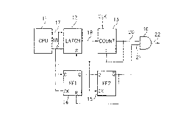
Referring now to the drawings there is shown in Figure 3 an
bodi~e~l of a trigger signal generating circuit according to the present
invention .
4 ~'
As shown in Figure 3, in the trigger signal generating circuit, a
counter 13 counts input clock pulses (CLK), and when the counter 13 counts
up to a pn:dt:l~""i"ed value, the counter 13 outputs a trigger signal 20. This
trigger signal 20 is input to a reset terminal R of a latch circuit 12 as a reset
5 signal and a load terminal L of the counter 13 as an initial value read-in
signal. In response to a trigger signal gt:nerdliol1 request output from a CPU
11 via an address bus 17 and a data bus 18, the latch circuit 12 outputs a
count start signal 19 to the counter 13. The CPU 11 is further adapted to
output a timing change request of a trigger signal geneldliol1 and a mask
10 request of the first trigger signal. The mask request output from the CPU 11
is also supplied to a data input terminal D and a clock input terminal CK of a
first flip-flop (FF1) 14 via the address bus 17 and the data bus 18. A normal
output signal of the first flip-flop 14 is supplied from a normal output terminal
Q of the hrst flip-flop 14 to a data input terminal D of a second flip-flop (FF2)
15. The trigger signal 20 output from the counter 13 is also input to a clock
input terminal CK of the second flip-flop 15. The second flip-flop 15 latches
the signal input to the data input terminal D and outputs an inverted output
signal as a mask request signal 21 from output terminal Q to one input
terminal of an AND circuit 16. The second flip-flop 15 also outputs the
20 inverted output signal as a clear signal to a reset terminal R of the first flip-
flop 14. The trigger signal 20 output from the counter 13 is also input to
another input terminal of the AND circuit 16. The AND circuit 16 calculates a
logical sum of the trigger signal 20 and the mask request signal 21 and
outputs the trigger signal 20 as a trigger signal 22 only when the mask
request signal 21 is a high level. The AND circuit 16 masks the trigger signal
20 when the mask request signal 21 is at a low level.
The operation of the trigger signal generating circuit described
above when the trigger signal generation timing is delayed will now be
5 described in detail in connection with Figure 4 which shows the waveforms of
the clock pulses (CLK) and the output signals of the counter 13, the hrst flip-
flop 14, the second flip-flop 15 and the AND circuit 16.
When the timing of the trigger signal generation is delayed, the
CPU 11 outputs a set signal of a smaller value than a normal predetermined
10 count value such as "100" as the timing change request of the trigger signal
generation as well as the mask request to the latch circuit 12 and the hrst
flip-flop 14 via the address bus 17 and the data bus 18. The latch circuit 12
outputs this set signal to the counter 13. In response to the set signal, the
counter 13 counts up to the smaller predetermined number of clock pulses
15 from a trigger signal A and generates a next trigger signal B to start counting
again from "0" to "100". The counter 13 then counts up to the 100th clock
pulse before generating a next trigger signal C in the same manner as the
conventional trigger signal generating circuit. In this case, when the counter
13 counts up to the predetermined number of clock pulses, the trigger signal
20 20 is supplied to a terminal of the AND circuit 16 and the load terminal of the
counter 13. Hence, the counter 13 starts to count clock pulses again from
"0". The trigger signal 20 is also supplied to the clock input terminal CK of
the second flip-flop 15.
On the other hand, in the first flip-flop 14, a high level signal "H"
is output from the normal output terminal Q for every clock pulse input via
the data bus 18, and the high level signal "H" is fed to the data input terminal
of the second flip-flop 15. In the second flip-flop 15, when the trigger signal
5 B is supplied from the counter 13 to the clock input terminal, a low level
signal "L" is output from the inversion output terminal Q to another input
terminal of the AND circuit 16. As a result, the AND circuit 16 outputs a low
level signal "L". That is, the first trigger signal B output from the counter 13
can be masked.
Further, the low level signal "L" output from the inversion output
terminal Q of the second flip-flop 15 is supplied to the reset terminal of the
first flip-flop 14 as the reset signal to reset the first flip-flop 14. Hence, the
first flip-flop 14 outputs a low level signal "L" from the normal output terminal
Q to the data input terminal of the second flip-flop 15. As a result, the
second flip-flop 15 outputs a high level signal "H" from the inversion output
terminal Q, to the AND circuit 16, and thus the AND circuit 16 outputs a high
level signal "H" as the trigger signal 22. That is, the second trigger signal C
output from the counter 13 is not masked and is output from the AND circuit
16
In the trigger signal y~n~ lg circuit of this embodiment, as
described above, owing to the mask request output from the CPU 11, the
first trigger signal B is masked and the second trigger signal C is output at
the delayed timing of the trigger signal generation.
As described above, according to the present invention, in the
trigger signal ye~ g circuit, since a trigger signal mask means for
masking the first trigger signal output from the counter is provided, even
when the timing of the trigger signal generation is delayed, a superfluous
5 trigger signal can be masked and thus the trigger signal can be generated
depend;"g on a pr~dt~ r~ ed delay time without outputting the superfluous
trigger signal.