Note: Descriptions are shown in the official language in which they were submitted.
WO92/07721 PCT/US91/059~8
2093003
THERMOGRAPHIC ELEMENTS
This invention relates to thermographic sheets
for direct thermal imaging and thermal transfer
imaging processes. In another aspect, this invention
relates to the use of antistick coatings in
thermographic sheets and a method of thermal transfer
imaging.
In thermal imaging or printing, images are
formed by heating heat-activatable materials in an
imagewise manner. Such heating is commonly conducted
by means of a thermal printhead, which consists of an
array of electrically heatable elements, each of which
is preferably activated by a computer in a time
sequence designed to produce imagewise heating. The
most common forms of thermal imaging are direct
thermal imaging and thermal transfer imaging.
In thermal transfer imaging processes, an image
is formed on a thermographic sheet known as a receptor
sheet by selectively transferring an image forming
material to the receptor sheet from another
thermographic sheet, known as the donor sheet, using a
thermal printhead. The three broad classes of thermal
transfer imaging processes are described in U.S.
Patent No. 4,853,365 (Jongewaard et al). Typically,
the donor sheet has a dye-donor layer disposed upon a
thin, flexible substrate such as paper or polymeric
film. Depending upon the type of thermal transfer
imaging process desired, the dye-donor layer may take
one of several forms, such as a meltable colored wax,
a diffusing dye, or heat-activatable reactants which,
when combined with other reactants incorporated into
the receptor sheet, form a colored compound.
Generally, in direct thermal imaging processes
a thermographic sheet having a dye-containing layer
containing colorless forms of heat-activatable dyes
and polymeric binder is heated in an imagewise manner
' '
.
.' , ,
w092/0772,1 ~g 3ù~ ~ PCT/US9l/0594~
by a thermal printhead. Upon application of heat, th~
colorless forms of the dyes are converted to their
colored forms so that an image is formed in the
dye-containing layer. Preferably, the thermal
printhead directlv contacts the dye-containing layer,
however, many of the dye-containing layers contain
compounds, such as the polymeric binder compounds,
which soften or melt and stick to the printhead
reducing printhead life and image quality.
Various materials have been described as being
useful as substrates for thermographic sheets. For
example, white-filled or transparent films of
polyester (e.g., polyethylene terephthalate (PET)),
polyethylene naphthalate, polysulphone, polystyrene,
polycarbonate, polyimide, polyamide, cellulose ester
(e.g., cellulose acetate and cellulose butyrate),
polyvinyl chloride and paper have been described as
useful. However, all of these materials have one or
more disadvantages which reduce their suitability as
substrates for thermographic sheets. For example, some
of the materials have glass transition temperatures
(Te) or melting temperatures (Tm) which are lower than
the temperature to which substrates would be heated
during thermal imaging processes, resulting in image
distortion. Some of the materials have poor optical
properties (e.g., high coefficient of birefringence,
high ~ haze or are inherently colored) rendering them
- unsuitable as substrates for certain thermal imaging
applications, some have poor film properties (e.g.,
poor tensile strength and elongation at break), some
have poor chemical resistance and some are
- hygroscopic.
Polyethylene terephthalate (PET) film has been
preferred for use as substrates in thermographic
sheets because it is a relatively low cost material,
it is available in various thicknesses and it provides
` relatively good optical clarity and tensile strength.
However, donor sheets made using P~T Eilm substrates
have a tendency to soften or melt and stick on the
. . .
WO92/07721 PCT/~S91/05948
3 2093003
thermal printhead, and friction between the PET film
and the prlnthead can result in reduced printhead life
and poor image quality. Generally, PET film of 4.5 to
6 micron thickness is used in donor sheets, but ~ET
film of such thickness tends to dimensionally distort
from the heat imparted by the printhead. Thus, donor
sheets made using PET film cannot easily be reused or
recycled, for example in thermal dye transfer
- processes. Since PET films of less than 4.5 micron
thickness tend to wrinkle and tear during the
thermographic element manufacturing process, e.g., on
coating lines, very thin films (i.e., less than 4.5
microns) are not particularly practical for use in
thermographic sheets.
One means of preventing sticking of the donor
sheet to the printhead has been to select substrate
materials which have softening temperatures higher
than those encountered by the donor sheet in the
printing process. For example, Japanese Patent
application No. J6 1246-093-A, describes the use of
copolymers containing acrylonitrile. However, none of
the proposed materials have displaced PET film as the
commercially preferred polymeric material for donor
sheets.
In order to reduce sticking of thermographic
sheets to the thermal printhead, antistick layers have
been applied to the surface of the donor sheet
contacting the thermal printhead and to the surface of
the heat-activatable dye layer on thermographic sheets
used in direct thermal imaging processes. For
example, low surface energy compounds, such as
fluoropolymers, silicones, waxes, fatty acids, and
metal stearates, have been described as antistick
coatings. Antistick compositions containing a low
surface energy compound and a polymeric binder having
a sufficiently high Ts so the binder does not soften
during the thermal imaging process have also been
described.
, ., ,: ~ . '
wo 92/0772 1 ~ `3, ~ . 4 PCT/US91/05948
One problem associated with the use of known
antistick compounds or compositions is that many of
the antistick compounds or compositions are not
readily soluble or dispersible in commonly used
organic solvents rendering such compounds or
compositions difficult to use. Although some
antistick compounds may be soluble in organic solvents
; and at the same time may exhibit antisticX behavior
(e.g., polymeric silicones), they may be very
migratory, i.e., they spontaneously spread along
surfaces for long distances, thereby contaminating
large areas of the coating facilities, as well as the
image-forming material and thermal imaging equipment.
Further, when donor sheets are stored in roll form,
some silicones may migrate from the side of the sheet
to which they have been applied to its opposite side,
where they may interfere with the thermal imaging
- process. Crosslinking or high degrees of
polymerization of silicone polymers may be helpful in
reducing migration, but because even small amounts of
uncrosslinked silicones can have a significant
negative effect upon imaging, it is difficult to
achieve sufficient crosslinking. Waxes may easily be
applied to the thermographic sheet, but they generally
contaminate printheads to an unacceptable deg~ee. One
additional disadvantage of using an antistick layer in
a thermographic sheet is that the application of such
a layer requires an additional coating step.
Thus, it would be desirable to use a material
as a donor sheet substrate which does not stick to the
thermal printhead or dimensionally distort upon
heating. However, such a material should also perform
about as well as PET film in donor sheets. It would
also be desirable to use, as an antistick layer, a
composition possessing antistick properties which does
not have the disadvantages of some of the compositions
described in the art.
.'`'
~ W092tO7721 PCT/US91/05948
~ 5 2C~3~3
In one aspect, this invention provides a
thermographic element (e.g., sheet or ribbon)
comprising at least two layers, wherein:
at least one of the layers comprises polymer
(hereinafter, for brevity, occasionally referred to as
FPE polymer), the polymer consisting or consisting
essentially of, repeating, interpolymerized units
derived from 9,9-bis-(4-hydroxyphenyl)-fluorene and
isophthalic acid, terephthalic acid or mixtures
thereof, the polymer being sufficiently low in
oligomer (i.e., chemical species having molecular
weights of about 8000 or less) content to allow
formatlon of uniform film; and
at least one of the layers is an imaging layer,
that is, a dye-donor layer, an image-receiving layer
or a heat-activatable imaging layer. Preferably the
FPE polymer has a narrow molecular weight distribu,ion
as measured by a polydispersition between 2 and 4.
In another aspect, this invention provides a
thermographic element useful as a donor element,
having a substrate layer comprising the FPE polymer,
and disposed on one of the major surfaces of the
substrate layer, a dye-donor layer, the dye-donor
layer being selected from any of those compositions
described as useful for dye-donor layers in thermal
transfer chemical reaction systems, thermal mass
transfer systems and thermal dye transfer systems.
In another aspect, this invention provides a
thermographic element useful as a donor element having
a substrate layer comprising material selected from
the group of materials consisting of paper and filled
or transparent films comprising polyester (other than
FPE polymer, for example, polyethylene terepthalate),
polysulphone, polystyrene, polycarbonate, polyimide,
polyamide, cellulose ester, and polyvinyl chloride
film, having disposed on one of the major surfaces of
the substrate layer, a dye-donor layer, the dye-donor
layer being selected from any of those compositions
~ .
.
~.
W092/07721 ~ PCT/US91/0~948
~e~cribed as useful for dye-donor layers in thermal
transfer chemical reaction systems, thermal mass
transfer systems and thermal dye transfer systems, and
having disposed on the other major surface of the
substrate layer, an antistick layer comprising the FPE
polymer.
In yet another aspect, this invention provides
a thermographic element useful in thermal transfer
printing processes as a receptor element, the element
comprising a substrate layer comprising the FPE
polymer and, having disposed on one of the major
surfaces of the substrate layer, an image-receiving
layer, the image-receiving layer being selected from
any of those compositions described as useful for
image-receiving layers in thermal transfer chemical
reaction systems and thermal dye transfer systems.
In yet another aspect, this invention provides
a thermographic element useful in direct thermal
printing processes, the element comprising a substrate
layer comprising the FPE polymer, and having disposed
on one of the major surfaces of the substrate layer, a
heat-activatable imaging layer. The heat-activatable
imaging layer may be selected from the group
consisting of any of those compositions described as
useful for heat-activatable imaging layers in direct
thermal imaging processes. In one preferred
embodiment of the thermographic element, the element
comprises a substrate layer comprising the FPE
polymer, having disposed on one of the major surfaces
of the substrate layer, a heat-activatable imaging
layer, and disposed upon the exposed surface of the
heat-activatable imaging layer, an antistick layer
comprising the FPE polymer.
When the dye-donor, image-receiving or
heat-activatable image layer is prepared from a
composition containing one or more compounds which can
act as solvents for the FPE substrate (e.g.,
tetrahydrofuran), the elements described above
optionally further comprise a protective layer
~, ,
..- -
,.
, . .
WO92/07721 7 2 ~ 9 3 ~ ~ ~ PCT/~S9l/0s948
disposed directly on the surface of the substrate
layer between the dye-donor, image-receiving or
heat-activatable imaging layer and the substrate
layer.
In yet another aspect, this invention provides
a method of thermal transfer imaging, the process
comprising the step of selectively transferring in an
imagewise manner an image-forming material from a dye
donor element (sheet or ribbon) to a receptor element,
the receptor element consisting of a film or sheet
comprising the FPE polymer.
In so far as is known, this invention is the
first to use the FPE polymer in thermographic elements
and imaging processes such as those described above,
and is the first to employ the many useful properties
of the FPE polymer (even when formed into very thin
films) in thermographic elements. Through this
invention thermographic elements have been prepared
using the FPE polymer which have advantages over
thermographic elements prepared from conventional
materials. It has now been found that the FPE polymer
can be used to prepare antistick compositions useful
for thermographic elements, and that such compositions
do not require additional low surface energy compounds
such as those described above. It has also been found
that an FPE film or sheet that is laminated or simply
laid upon the surface of a thermographic element is an
effective antistick layer. Such a construction has
the further advantage that if the FPE film is only
temporarily laminated or laid upon the element it may
be removed after imaging and reused. Representative
values of some of the useful physical and chemical
properties of the FPE polymer are summarized in
TABLE-l.
- : .
~, ' - ' : .
, ~ .
PCT/I,IS91/05948
WO92/07721
TABLE-1
COMPARATIVE ~ ES
PROPER~Y VAL~E
FPE _ _ PET
Tm ~C) None 260
ASTMD-793
T~ (C) 330 80
Shrinkage Q200C (%) <0.2 4.3-8.0
. Moisture coefficient
of expansion
(m/m/% R.H.) 0.8 x 10⁵ 1.3 x 10⁵
Heat of distortion (%)
ASTMD-1637 <<0.1 (21-300C) N/A
for 50 psi load
, 1.0 (21-300C)
!~ 25 for 300 psi load
Coefficient of friction (%)
ASTMD-1894
~ /~, (starting) 0.4-0.6 0.4-0.6-
- 30 ~y (kinetic) 0.4-0.6 0.4-0.6--
.,
Coefficient birefringence- 0.0003 0.01-0.1
Haze (%) 0.1 0.4-0.8
~s~D-1003
' WO92/07721 2 o 9 3 o o 3 PCTIUS91/05948
*Data is not available for PET because the polymer
melts at a temperature within the test range.
Film contained no slip agents.
Film contained slip agents, without slip agents may
have coefficients of friction of 2 or more.
' Measured using a Gaetner Babinet compensator.
.. : .
~ . '-~ ' - - ~
WO92/07721 ~3~U; lo PCT/US91/05948
The invention is described in detail
hereinafter with reference to the accompanying
drawings in which:
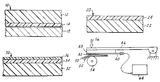
FIG. l is a cross-sectional view of one
embodiment of a donor element of the present
invention.
FIG. 2 is a cross-sectional view of one
embodiment of a receptor element which may be employed
in the present invention.
i 10 FIG. 3 is a cross-sectional view of one
embodiment of a thermographic element of the present
invention used ~or direct thermal printing.
FIG. 4 illustrates one method by which a
receptor element can be imaged and by which the
materials of the present invention can be tested.
FIG. 1 depicts a donor element 10 suitable for
use in a thermal transfer printing process. Donor
element 10 comprises a substrate layer 12, comprising
the FP~ polymer. Optionally, the substrate layer 12
further comprises a small amount (e.g., 5 weight
percent or less) of a slip compound such as silicon
dioxide, aluminum silicate, aluminum oxide, calcium
carbonate or fused silica. The substrate layer 12
may, if desired, also further comprise white or
colored fillers. Many of such fillers known in the
art are useful in this invention. The substrate layer
12 may be used in a sheet size embodiment or in a
continuous roll form such as a continuous web or
ribbon. A dye-donor layer 14 comprising any of the
image-forming compositions described as useful for
thermal transfer chemical reaction, dye transfer or
mass transfer imaging processes is disposed on one of
the major surfaces of the substrate layer 12.
Hereinafter, the major surface of the substrate layer
12 carrying the dye-donor layer 14 will be called the
front side of the donor element 10. The opposite
major surface of the substrate layer 12 will
hereinafter be oalled the baok side of donor element
:' ,
.
- WO92/07721 PCT/~'S91/0~948
lO. Because of the high T~ and excel~ent surface
properties (e.g., low coefficient of friction) of the
substrate layer 12, no antistick layer need be applied
to the back side of the donor element 10 to prevent
sticking of the donor element 10 to a thermal
printhead.
- Typically, the substrate layer 12 is in the
form of a film comprising FPE polymer. The film
generally has a thickness of less than about 20
microns, preferably 6 microns or less, and most
; preferably 4.5 microns or less. Since thinner donor
elements generally result in higher thermal transfer
imaging process efficiencies, very thin donor films
(e.g., 1.5 to 3 microns in thickness) are generally
very desirable. In contrast, many of the polymeric
films which have been described as useful for
thermographic elements are not currently available-in
thicknesses of less than 6 microns, and those which
are available have other disadvantages which render
them less desirable for use in donor elements than FPE
film. For example, 4.5 micron PET film is generally
difficult to handle on thermal transfer imaging
equipment because it can tear, dimensionally distort
upon application of heat from the printhead, or melt
and stick to the printhead in the absence of an
antistick layer.
The composition of the dye-donor layer 14 will
depend upon the thermal transfer imaging process
desired, and many of the compositions known in the art
may be used in this invention (e.g., U.S. Patent Nos.
4,853,365 ~Jongewaard et al.), 4,847,238 (Jongewaard
et al.), 4,822,643 (Hsin-Hsin et al.) and 4,839,224
(Hsin-Hsin et al.). Briefly described, the dye-donor
layer 14 typically comprises a meltable wax or
meltable polymeric material, to which colorants and
other additives to improve transferability have been
added. Suitable colorants and additives are well
known to one of ordinary skill in the art.
Alternatively, the dye-donor layer 14 can comprise a
W092/07721 ~J~ 12 PCT/US9l/05948
sublimable dye or other colorant which is transferabl~
upon applicatior, of heat. Alternatively, the
dye-donor layer 14 can comprise at least one chemical
substance which, upon application of heat, is
transferred to a receptor sheet 18 and reacts with
other ~aterials contained on the receptor sheet 18 to
form a colored compound, which colored compound is
then retained on the receptor sheet 18 forming an
image. Examples of this mode of image formation
include systems in which the leuco form of a dye is
incorporated into the receptor sheet 18, and a
phenolic compound is incorporated into the dye-donor
layer 14. Upon heating, the phenolic compound
diffuses into the receptor sheet 18, and converts the
1~ leuco form of the dye to its colored form to create an
image. Alternatively, the leuco form of the dye can
be contained in the dye-donor layer 14, from which it
then diffuses, upon heating, into the receptor sheet
18, to react with an activating agent contained
therein.
The dye-donor layer 14 can comprise two or more
distinct layers, for example, the layer nearest the
substrate layer 12 can be a heat-activated release
layer, the next layer can contain a colorant, and the
outermost layer may be formulated to improve adhesion
of the colorant to the receptor.
.
:
W092/0772l 13 2 ~ `9 ~ ~ ~P3CTtUS91/05948
! The dye-donor layer 14 is generally applied to
the substrate layer 12 in the form of a solution or
dispersion of the components of the dye-donor layer in
an organic solvent. If the solution or dispersion
applied to the substrate layer 12 contains one or more
compounds which act as solvents for the FPE polymer
(e.g., tetrahydrofuran (THF), 1,2-dichloroethane
(DCE), N-methylpyrrolidone (NMP), cyclohexanone and
methylene chloride), a protective layer (not shown) is
preferably provided between the dye-donor layer 14 and
the substrate layer 12. The protective layer is
chemically resistant to the compounds acting as
solvents for the FPE polymer and may be provided by
any process render ng the surface of the FPE substrate
layer 12 chemically resistant to the solvent(s). For
example the surface of substrate layer 12 can be
coated with a chemically resistant coating or it can
be otherwise treated to render it chemically
resistant. One chemically resistant coating
composition comprises certain branched acrylic
monomers which are "graft-polymerized" to the FPE
substrate layer using actinic radiation. Some of the
branched acrylic monomers can be selected from the
group consisting of trimethylolpropanetriacrylate
(TMPTA), pentaerythritoltetraacrylate (PET4A),
dipentaerythritolhydroxypentaacrylate (DPOPA),
N,N-dimethylacrylamide (DMA), and
tetraethyleneglycoldiacrylate (T4EGDA). Typically, the
chemically resistant coatings are one micron or less
in thickness, more preferably, these coatings are 0.5
micron or less in thickness, e.g., 0.3 to 0.5 ~icron.
Alternatively, the protective layer may result from a
surface treatment of the substrate layer 12 rendering
it more chemically resistant, e.g., by cross-linking
or crystallizing molecules located at the surfaces of
the substrate layer. For example, controlled exposure
of the surface of the FPE substrate layer to actinic
radiation, e.g., using an electron-beam, laser or W
lamps can render the surface more chemically
W092/0772l Q3 PCT/US91/05948
re~ ~ant Processes useful to treat the surface of
the FPE substrate layer to render it more chemically
resistant to solvents are described in U.S. Patent
Nos. 4,879,176 (Ouderkirk et al), 4,822,451 (Ouderkirk
; 5 et al), and 4,~02,378 (Ouderkirk et al).
In another embodiment of a donor element of
this invention, instead of FPE polymer, the substrate
layer 12 comprises one of the materials described in
; the art as useful for this purpose. Representative
examples of such materials include films of
transparent or filled polymers such as polyester
other than the FPE polymer, polyethylene napthalate,
polysulfone, polycarbonate, polyimide, polyamide,
cellulose ester and paper. Since such a substrate
layer 12 would not possess the high T~ and low
coefficient of friction of an FPE substrate layer, an
antistick layer (not shown) comprising FPE polymer is
disposed on the back side of the substrate layer 12.
The antisticX layer may be a film or sheet
comprising or consisting essentially of FPE polymer.
Optionally, the film or sheet may further comprise a
slip compound such as those described above. The film
or sheet may be permanently or temporarily laminated
together with the remaining portion of the donor
element, for example, by using an adhesive, preferably
: a pressure sensitive adhesive or a compatible
polymeric binder, which will remain flexible and
provide adhesion even at imaging temperatures.
Examples of compatible polymeric binders may include
polyvinylacetate, cellulose derivative, cellulose
acetate butyrates, polyvinyl butyrates, vinyl polymers
and vinyl copolymers. Alternatively, the layers may
be held together using a mechanical fixture, or by
heating the donor substrate layer to its softening
temperature, laminating the FPE film to the substrate
layer and cooling the construction.
The antistick layer can also comprise FPE
polymer and a~ least one binder polymer. In this
instance, the antistick layer is applied to the
'~ '
- WO92/07721 2 ~ 3 ~ ~ ~ 3 PcT/us91/05948
surface of the donor substrate layer by cooling a
solution or dispersion of the component of the
antistick layer in an organic solvent and drying the
coating. The blnder polymer must not adversely affect
S the antistick properties of the FPE polymer, must
improve the adhesion of the antistick layer to the
donor element, and must not scratch, erode,
contaminate, or otherwise damage printheads, or harm
image quality. Both the FPE polymer and binder
polymer must be soluble or dispersible in a common
solvent or dispersing agent. Examples of such
solvents include, but are not limited to THF, DCE,
methylene chloride, cyclohexanone, NMP, and blends of
such solvents with other common organic solvents such
as methyl ethyl ketone (MEK). Many of the blnder
polymers described as useful in antistick compositions
are also useful in this invention. For example,
polymethacrylates, polyvinyl stearates, polyesters,
chlorinated polyvinyl chlorides, acrylonitriles,
styrenes, styrene-butadiene elastomers,
ethylene-propylene elastomers, poly(vinyl
alcohol-co-butyrol), poly(vinyl alcohol-co-acetal),
polyvinyl acetate, cellulose acetate butyrate,
cellulose acetate and ethyl cellulose are useful in
2 3 this invention.
Generally, the FPE polymer comprises lO to 100%
by weight of the antistick layer. If the antistick
layer further comprises one or more binder polymers,
then the antistick layer preferably comprises at least
50 weight percent FPE polymer. The amount of binder
polymer used in the antistick must be sufficient to
result in adhesion of the antistick layer to the
substrate layer 12, but typically, the binder polymer
will be employed at levels of 90 to 10% by weight of
the antistick layer. If the binder polymer has a
sufficiently high T~ not to soften or melt at thermal
imaging process temperatures, a somewhat larger amount
of binder polymer can be used in the antistick layer.
For example, in some cases, up to a 2 to l weight
.:. :
.~
WO92/07721 ~b~ ' 16 PCT/~'S91/0594X
ratio of FPE polymer to binder polymer can be employe~
in the antistick layer. Examples of binder polymers
which may be employed at these higher levels include
polyvinylstearates, acrylonitriles and
ethylene-propylene elastomers.
: The antistick layer may additionally contain
filler materials and other additives, provided such
materials do not inhibit the antistick features of the
antistick layer, and further provided that such
materials do not scratch, erode, contaminate, or
otherwise damage printheads, or harm image quality.
It is preferred that the concentration of such fillers
and other additives be kept below about 5% by weight,
though the maximum permissible concentration depends
upon the particular filler used. Fillers suitable for
the antistick layer of this invention include
crystalline polymeric particulate material,
crosslinked polymeric particulate material,
non-migratory polymeric particulate material having
low surface energy, and non-abrasive inorganic
materials. Fillers that are particularly suitable in
this regard include amorphous fumed silica (e.g.,
"SYLOID", available from W.R. Grace & Co.) and
urea-formaldehyde particles of submicron size
agglomerated into particles of about 5 to 6 micron
diameter (e.g., "PERGOPA~ M2", available from
Ciba-Geigy), and submicron-sized aluminum oxide
particles. Addition of such particulate materials has
the desirable effect of reducing the coefficient of
- 30 friction of the antistick layer.
Non-particulate additives suitable for the
antistick layer of this invention include surfactants,
antistatic agents, lubricants, plasticizers, and other
modifiers, provided that such additives do not
contaminate or damage the printhead and do not have a
deleterious effect upon the imaging capabilities of
the donor element l0 or receptor sheet 18.
FIG. 2 depicts one embodiment of a receptor
element which may be used in this invention. The
WO92/07721 17 2 ~ 3 3 ~ o 3PCT/US91/0s948
receptor element 20 comprises a substrate layer 22,
having disposed on one of its major surfaces,
image-receiving layer 24.
The substrate layer 22 can comprise FPE
polymer, generally in the form of a sheet or film,
which optionally may contain a small amount (e.g., 5
weight percent or less~ of one of the slip compounds
described above and white or colored fillers. The
substrate layer 22 may be used in a sheet size
embodiment or in a continuous roll form such as a
continuous web or ribbon, however, for most
applications, a sheet size embodiment is preferred.
Typically, the substrate layer 22 has a thickness of
0.05 to 5 mm (2 to 200 mils), however, because of the
excellent strength of the FPE polymer film, the
substrate layer 22 can be less than 0.05 ~m (2 mils)
thick, may be less than 6 microns thick, and even `ess
than 3 microns thick. The FPE film provides
advantages over materials currently used as receptor
element substrate layers because it possesses a low
birefringence coefficient, low percent haze, is
colorless, relatively unreactive with compounds
comprlsing the dye-receiving layer and nonhygroscopic.
Thus, it provides advantages when employed in receptor
elements requiring transparent substrates, such as
receptor elements used as overhead transparencies
after they have been imaged. It also has low
reactivity with components of any image-receiving
layer and low hygroscopicity resulting in longer
- 30 receptor element shelf life. The composition of
the image-receiving layer 24 will depend upon the
thermal transfer imaging process selected and the
chemical composition of the dye-donor layer of the
donor element used in conjunction with the receptor
element in the thermal transfer imaging process. Many
of the compositions ~nown in the art are suitable in
this invention (e.g., U.S. Patent No. 4,853,365
(Jongewaard et al.) incorporated herein by re~erence).
The image-receiving layer 24 of the receptor element
; WO92/07721 q ~33~ 18 PCT/~S91/05948
20 can comprise at least one chemical substance which,
reacts with other materials transferred upon
application of heat from the dye-donor layer of a
donor element to form a colored compound, which
colored compound is then retained on the receptor
element 20 forming an image such as the leuco dye and
phenolic-compound system described hereinabove.
When the composition used to prepare the
image-receiving layer 24 contains one or more
compounds which also act as solvents for the FPE
polymer a protective layer (not shown), as described
above, preferably is provided between the
image-receiving layer 24 and the substrate layer 22.
If the substrate layer is selected from the group
consisting of materials described in the art as useful
for this purpose (c.g., paper and filled or
transparent film of polyester (other than FPE polymer) -
polyethylene naphthalate, polysulfone, polycarbonate,
polyimide, polyamides and cellulose ester), then the
image-receiving layer 24 comprises in addition to the
other ingredient commonly used in compositions for
thermal dye transfer, thermal chemical reaction and
thermal transfer systems up to about 50 weight percent
FPE polymer. The FPE polymer then provides improved
slip or antistick properties to the image-receiving
layer and may improve the adhesion of the dye or
pigment to the receptor element.
FIG. 3 depicts one embodiment of a
thermographic element of this invention which is
; 30 useful in direct thermal imaging processes. This
thermographic element 30 comprises a substrate layer
32, having disposed on one major surface a
heat-activatable image-forming layer 34. Optionally,
an antistick layer 36 may be disposed on the exposed
surface of the image-forming layer 34. Substrate
layer 32 can be selected from materials from the group
consisting of paper and, transparent or filled, films
of polyester (other than FPE polymer~, polyethylene
napthalate, polysulfone, polycarbonate, polyimide,
::
"0-
:. ' -:.
,
WO92/07721 PCT/~'S91/059~8
- 19 2as3~
polyamide and cellulose ester, but preferably,
substrate layer 32 comprises FPE polymer. Optionally,
the substrate layer 32 may further comprise a small
amount (e.g., 5 weight percent or less) of one of the
slip compounds described above, or, if desired, white
or colored fillers. The substrate layer 32 may be
used in a sheet size embodiment or in a continuous
roll form such as a continuous web or ribbon, however,
for most applications, a sheet size embodiment is
preferred. Generally, the thickness of the substrate
layer 32 will vary depending upon how the
thermographic element 30 will be used after imaging.
Typically, the substrate layer 32 comprises FPE film
having a thic~ness of 0.05 to 5 mm (2 to 200 mils),
however, because of the strength of FPE film, the
substrate layer 32 can be less than 0.05 mm (2 mils)
thick, may be less than 6 microns thick, and even less
than 3 microns thick. The FPE film has advantages
over materials currently used in thermographic
elements used in direct thermal printing because it
possesses a low birefringence coefficient, low percent
haze and it is colorless. Thus, it provides
advantages over conventional substrate materials when
employed in applications requiring transparent
substrates, e.g., overhead transparencies. The FPE
film is also relatively unreactive with compounds
comprising the heat-activatable imaging layer and is
nonhygroscopic. Thus, it also provides advantages
over conventional substrate materials even in
;~ 30 applications that do not require transparent
substrates because the low reactivity and low
hygroscopicity of the FPE film can result in longer
element shelf life.
Heat-activatable imaging layer 34 may comprise
any thermally sensitive image-forming composition
useful in direct thermal imaging processes. Many
compositions described as useful for this purpose can
be used in this invention (e.g., U.S. Patent Nos.
4,910,186 (Whitcomb) and 4,808,565 ~Whitcomb et al).
.
:
,... .. ". ~ , - . .
;. '
`~ - , ' :
'
- wog2/07721 ~S~39 20 PCT/US91/0594X
Some useful compositions comprise a polymeric binder,
a leuco dye and a heat activatable color developing
agent, such as, for example, an acid-sensitive leuco
dye and a thermally releasable acid.
The antistick layer 36 may comprise any of the
antistick compositions described as useful in direct
thermal transfer or thermal transfer imaging processes
(e.g., Japanese Kokai No. 7467/1980 and 49638/1989,
U.S. Patent Nos. 4,592,945 and 4,572,860 U.S. Patent
Application Serial No. 326,300 and Japanese Patent
Application No. 60-22~794A2). However, preferably the
antistick layer 36 comprises FPE polymer as described
above. However, if an FPE film is used as an antistick
layer, any adhesive or compatible polymeric binder
used to laminate the FPE film to the heat-activatable
imaging layer must permit the FPE film to adhere to
the dye layer either permanently or temporarily as
desired and must not react with the dye layer. Heat
could also be used to laminate the FPE film to the dye
layer, for example by heating the thermographic
element until one or more of the binder polymers in
the dye layer softens, laminating the film together
with the element and cooling the element.
The dye-donor, image-receiving,
heat-activatable imaging, protective, and antistick
layers described above can be applied to the
thermographic elements by means known to one of
ordinary skill in the art. A particularly useful
method of applying such layers involves the steps of
dissolving or dispersing the components of the
particular layer in a suitable organic solvent, or if
appropriate, in water, and applying the resulting
solution or dispersion to the element by means of a
- conventional solution coating apparatus, such as a
wire-wound rod (Mayer rod), knife coater, extrusion
coater, rotogravure coater, dip coater, electro-spray
coater, kiss coater or other conventional coater,
followed by drying the applied coating with heated air
in a controlled manner to minimize curling of the
.
'~ ' ' . .
W092/07721 2 o ~ 3 ~ PcT/~ls9l/0s948
thermographic element. The thickness of the resulting
coating can be controlled by controlling the viscosity
of the solution or dispersion, and by controlling the
amount of the solution or dispersion applied to the
S element. Typically, antistick coatings are less than
2 microns thick after drying, and preferably are less
than one micron thick. Dye-donor, dye-receiving and
heat-activatable dye layers are generally less than
0.025 mm (1 mil) in thickness after drying. As stated
above, the protective layer is generally 1 micron or
less in thickness.
The FPE polymer useful in this invention is
described and can be prepared using the method
described in U.S. Patent No. 4,967,306. FPE polymer
used to prepare the thermographic elements and the
antistick layers described above generally have a
weight-average molecular weight of at least 500,000
and preferably about 700,000 or 900,000 or higher.
Preferably the FPE polymer used in this
invention has a narrow molecular weight distribution,
is measured by polydispersivities of 2 to 4. The
polymer is preferably prepared from
9,9-bis(4-hydroxyphenyl)fluorene and a mixture of the
isophthalic or terephthalic acid chlorides. The
isophth21ic and terephthalic acid chloride are
preferably employed in a ratio of 70 to 30 parts by
weight of terephthalyl chloride to 30 to 70 parts by
weight of isophthalyl chloride. Most preferably, an
equimolar mixture of terephthalyl chloride and
isophthalyl chloride is employed in this invention.
Briefly, the FPE copolymer can be prepared by
preparing a mixture of
9,9-bis-(4-hydroxy-phenyl)-fluorene (at least 99.8
pure), an alkaline metal hydroxide such as sodium
- 35 hydroxide, distilled water, and an organic cosolvent
such as dioxane or acetone. A 2.3 to 1 molar ratio of
sodium hydroxide to 9,9-bis-(4-hydroxyphenyl)-fluorene
is generally employed. The organic cosolvent need not
be anhydrous, however if dioxane is used, preferably
.
.: . .
?~ ~
W092/07721 q ~ ~ 22 PCTtUS91/05948
it should be stripped of peroxide compounds (e.g.,
passing it through a molecular sieve). The resulting
mixture is heated to its boiling point (or preferably
simply stirred), cooled to room temperature, and
charged into an appropriate reaction vessel equipped
with a high speed stirrer and thermometer. Preferably
the reaction vessel is equipped with a cooling jacket.
With stirring, a -oom temperature solution of a phase
transfer catalyst, preferably benzyl triethyl ammonium
chloride, dissolved in distilled water is added,
followed by a chilled, organic solvent such as
l,2-dichloroethane or methylene chloride. It is
advantageous to chill the organic solvent. To the
stirred mixture, another mixture containing an
equimolar amount of isophthalyl chloride and
terephthalyl chloride in an anhydrous, organic solvent
such as l,2-dichloroethane is added. Stirring is
continued while the reaction proceeds. When the
reaction has reached the desired degree of completion,
the pH of the reaction mixture may be adjusted such
that it is acidic, preferably to a pH of about 3 to 4.
Alternatively, the reaction mixture may be allowed to
separate into an aqueous phase and an organic phase,
the aqueous phase is decanted and the pH of the
organic phase adjusted as described above. The
organic phase contains the FPE polymer. If necessary,
~ additional l,2-dichloroethane may be added to the
- organic phase to reduce the solution viscosity to
allow stirring. The resulting organic phase is then
mixed with approximately an equal volume of deionized
water to extract water soluble impurities, such as
ionic impurities, from the organic phase. The water
and dissolved impurities are allowed to separate from
the organic phase and are decanted. This procedure is
repeated until the conductivity of the decanted water
is 20 ~mho or less. After the final washing step, the
- FPE polymer is precipitated from the organic phase by
stirring into the organic phase an excess
(approximately two times the organic phase volume) of
WO92/07721 23 2 ~ 9 $ ~ ~ ~PCT/US91/05948
an organic solvent with selective solubility, that is,
an organic solvent in which the oligomeric species are
soluble but the ~olymer is not soluble. The preferred
organic solvents for precipitation are the lower
ketones containing 3 to 10 carbon atoms, more
preferred are those containing 3 to 5 carbon atoms
such as methyl ethyl ketone. The most preferred
organic solvent for precipitation is acetone.
Optionally, the precipitated polymer may be washed
with distilled water.
Substrate layers 12, 22 and 32 comprising FPE
polymer are prepared by casting FPE polymer dissolved
in a suitable organic solvent onto a suitable casting
substrate (e.g., a stainless steel belt) using any of
the solution coating methods described above,
evaporating the solvent and removing the resulting
film from the casting substrate. The thickness of.the
resulting film can be controlled by controlling the
viscosity of the FPE polymer solution and the amount
of the solution applied to the casting substrate.
Optionally, a small amount (i.e., less than about 5
weight percent of the casting solution and preferably
less than about 2.5 weight percent of the casting
solution) of a slip compound, such as those described
above, may be added to the casting solution. Suitable
organic solvents for the preparation of FPE polymer
films include, but are not limited to, cyclohexanone,
methylene chloride, and 1,2-dichloroethane. NMP is
not ~a preferred solvent because FPE films cast from
solutions made using NMP are somewhat hazy.
As stated above, the unique properties of the
FPE films permit the use of thinner films in donor,
receptor and direct thermal imaging elements than
could have been achieved using conventional materials.
FPE films as thin as 3.0 microns can be transported
through direct thermal and thermal transfer printers
without tearing, curling, sticking or jamming.
- The following non-limiting examples are
provided to further illustrate the invention.
;
,,. -.. .
, .
' ' ' '
WO9~/07721 ~3~ 24 PCT/~591/03948
EXAMPLES
In the following Examples, thermographic
elements are evaluated using an apparatus, such as
that depicted in FIG. 4, which approximates the
conditions encountered in commercially available
thermal transfer printing machines. The apparatus
consists of the following elements
1. Thermal printhead 40, having heated
printing elements 42, of a type used in commercially
available thermal printing machines.
2. Electronic circuitry 44, capable of driving
thermal printhead 40 in the manner prescribed by the
1~ printhead manufacturer, with the additional capability
of varying the voltage driving the printing elements
42 of thermal printhead 40. The circuitry also
includes means provided for measuring the voltage
provided to printhead 40.
3. Mechanical fixture 46 and heat sink 48 for
holding thermal printhead 40 in such a position that
printing elements 42 remain in contact with donor 50
and receptor 52 during the printing process.
. Drive roll 54 for advancing the
image-forming materials past the printhead as printing
takes place.
: The printhead 40 is held against rubber drive
roll 54 having a Shore hardness of 40 to 50, as shown
in FIG. 4. Imaging pressure is determined by the
force applied in holding printhead 40 against rubber
drive roll 54, represented by weight 56. Donor 50 and
receptor 52 were sandwiched together and driven past
printhead 40 by rotation of drive roll 54. Electronic
circuitry 44 supplying the imaging signal to the
printhead 40 provides a square wave pulse signal known
as the burn profile of the imaging signal. The height
of the square wave pulses, hereinafter called the
pulse voltage, is adjustable to values both above and
` below a nominal value.
. . .
- WO92/07721 25 2 ~ 9 3 ~ o ~CT/US91/0594
-``` Fixture 46 for holding the printhead during
use, and the apparatus for transporting donor 50 past
printing elements 42 are constructed in accordance
with the specifications provided by the printhead
manufacturers to closely approximate the conditions
encountered in commercial applications of the
printhead.
The following Examples employ a Kyocera model
KMT-128-8MPD4-CP raised glaze thin film thermal
printhead, having 8 dots/mm and 0.3 watts/dot. The
imaging pressure of the thermal printhead is 2.0 Kg
distributed over the 128 mm printhead width unless
stated otherwise.
EXAMPLES 1 to 4 and COMPARATIVE EXAMPLE lC
These Examples illustrate the effectiveness of
~ antistick layers comprising FPE polymer.
; Mixtures are prepared of the formulations
described in TABLE-2. The mixtures are then coated
onto one side of 6 micron Teijin Type F24G PET film
(available from Teijin) to a wet coated thickness of
about 18 microns (0.,72 mil) using a number 8 Mayer
bar. The coated films are then dried by means of
forced heated air.
; The films, now coated on one side, are each
transported through the test apparatus with a receptor
sheet of thermal dye transfer paper commercially
available from DaiNippon Printing Company. The
printhead is operated for each antistick coating at a
series of predetermined head voltages and a 23
millisecond pulse rate. The printhead is initially
run at low voltages, and then at successively
increasing voltages, while applying print signals to
all the segments of the printhead at the rate used to
print solid coverage of the receptor. These
conditions are used because sticking is most severe
when the printhead is printing a solid bar running the
full width of the printhead and every element of the
:
" ~ :
W092/0772l ~93~ 26 PCT/~'S91/05948
printhead is activated at every position on the sheet -
to be imaged. In these examples, the head voltage is
varied from 9 to 20 volts. This approximately
corresponds to energies of 4.0 to 18.6 Joules/cm2.
Performance of the antistick coatings is
evaluated by noting (a) smoothness of transport
through the test apparatus, including degree of
tearlng or ripping, (b) noise level during transport,
and (c) contamination of the printhead. High noise
levels are taken to be an indication of partial
sticking, which indicates that the level of
performance is unacceptable. In order to be judged
' acceptable, the donor and receptor sheets must
I transport through the test apparatus without noise at
least up to a 16V (13.21 Joules/cm2) head voltage
level.
The antistick layers made using the
compositions of Examples 1 to 4 transport smoothly
through the test apparatus, producing minimal or no
noise at head voltages of 16V or more, without causing
stoppage, jamming, tearing, or ripping of the film in
the apparatus, and with minimal or no contamination of
the printhead at all of the energy levels applied by
the printhead indicating that all of the compositions
comprising FPE polymer and a binder polymer perform
effectively as antistick compositions.
The film coated with the antistick composition
lC (described in TABLE-2) flakes off when passed
through the test apparatus indicating poor adhesion of
the antistick layer to the PET film.
The test compositions and the maximum head
voltages producing minimal or no noise are summarized
in TABLE-2.
'"
., .
W092/0~21 2 0 ~ 3 PCT/~S91/05948
TABLE-2
ANTISTICK COATING COMPOSITIONS
EXAMPLE COMPOU.ND~ AMOUNT VOLT
(q) (V~
lC FPE polymer 5
Tetrahydrofuran 100 _ '
1 FPE polymer 4.0
VitelTM PE 200 1.0 18
Tetrahydrofuran 195
2 FPE polymer 4.0
; Polysar~M 346~ 0.6
Toluene 19.4 20
. Tetrahydrofuran 76.0
:
3 FPE polymer 4.0
VitelTM PE 200' 0.5
: PolysarrM 346b 0.9 20
. Toluene 29.1
Tetrahydrofuran 135.5
` 4 FPE polymer 4.0
VitelTM PE 200' 1.0
PolysarTM 346b 0.9 18
Toluene 29.1
Tetr-hydrofuran 195.0
.
~.
. .~ .
'
WO92~07721 ~ 28 PCT/US91/05948
^ VitelTM PE 200 is a polyester resin available
from Goodyear Chemical Corporation.
b PolysarT~ is a random copolymer of ethylene
and propylene, and is available from Polysar
International.
c Voltage was not measured due to poor adhesion.
0 d FPE polymer having a polydispersity of 2.2 is
used in Examples l to 4 and Cl.
,~
,;
, . .
:,
,,-~
- .
-
- WO92/07721 PCT/~'S91/05948
20930~
EXAMPLES 5-6
The following Examples illustrate the antistick
effectiveness of FPE film with slip agents. Two
casting solutions containing FPE polymer and silicon
dioxide are prepared. Both casting solutions are
prepared using FPE polymer having a polydispersivity
of 2.9. Film A is cast using a solution containing 3.5
weight percent FPE polymer, 2.5 weight percent silicon
dioxide and the remainder, methylene chloride. Film B
is cast using a solution containing 3.5 weight percent
FPE polymer, 5 weight percent silicon dioxide and
methylene chloride. The casting solutions are hand
cast using a knife coater and dried using hot forced
air. The dried thickness of film A and film B is
nominally 8 microns.
Films A and B are each transported through the
test apparatus with a receptor sheet of thermal dye
transfer paper used as a support and aid in feeding
the thin film through the test apparatus. The thermal
transfer paper is commercially available from
DaiNippon Printing Company. The printhead is operated
in accordance with the procedure described in Examples
1 to 4 except that 5Kg imaging pressure is used. The
DaiNippon paper is generally imaged at 16V (13.21
Joules/cm2).
Both FPE films transport smoothly through the
: test apparatus, producing minimal or no noise at head
voltages of 16V or more (in fact film A only starts to
produce a minor amount of noise at 20V and film B
produces no noise at 20V), without causing stoppage,
jamming, tearing, or ripping of the film in the
apparatus, and with minimal or no contamination of the
printhead at all of the energy levels applied by the
printhead. These results indicate that the FPE films
have antistick properties and perform effectively as
donor element substrate layers without requiring an
antistick layer.
.
. .
~ '' ~ ' '" .
:: :
- W O 92/~7721 PCT/US91/05948
3 EXPiMPLE 7
A 10 microns thick film is prepared by casting
a 4.5 weight percent solution of FPE polymer (having a
weight average molecular weight of 727,000 and a
polydispersivity of 2.2) in methylene chloride and
drying the casting. The film is then coated with a
coating consisting of 25 weight percent
trimethylolpropanetriacrylate dissolved in acetone by
wiping a thin coating of the solution on both sides of
i the film. After air drying, each side of the film is
passed under 2 W lamps under a nitrogen at~osphere at
a rate of 50 ft/min. The wattage of the W lamps is
200 watts/in.
- 15 Donor elements are prepared from the coated
film by applying a composition comprising the
components of a dye-donor layer which are dissolved or
dispersed in organic solvent. The composition used to
prepare the dye-donor layer is summarized in Table II.
The composition is applied to one side of each element
using a number 8 Mayer bar. The wet thickness of each
of the coatings is 1. 8 X 103 cm (0.72 mil). The
coated elements are then dried using forced hot air.
, One of the donor element is placed in contact
- 25 with a commercially available base receptor sheet from
DaiNippon. The thermal printhead described above is
operated in accordance with the procedure described in
Examples 1 to 4. The other donor element is placed in
contact with a receptor sheet, the receptor sheet
being prepared by coating a 1.8 x 10⁻³ cm (0.72 mil)
coating of the image-receiving composition (summarized
in Table III) onto one surface of a 0.01 cm (4 mi~)
thicX PET film using a number 8 Mayer bar and forced
air drying the resulting coating.
Each of the donor elements are passed through
the thermal transfer printing apparatus. Both donor
elements transport smoothly through the test
apparatus, producing minimal or no noise at head
voltages of at least 21 volts, causing no stoppage,
-
~ . :: `,
.~
W092/07721 2 PcT/uSgl/0s94~
jamming, tearing, or ripping of the film in the
apparatus, and with minimal or no contamination of the
printhead at all of the energy levels applied by the
; printhead. However, the image transfer density of
each of the formed iinages was low. This is probably
due to the thickness of the FPE film. These results
indicate that the FPE films are useful as donor
~lement substrates in thermal transfer imaging
processes.
:' ' ~ ' ' : '' ' -
...
.
WO92/07721 PCT/US91/05948
32
TABLE II
DYE-DONOR LAYER
Ingredients Amount
(g)
, Anthraquinone dye' 6.0
Azo dyeb 0.9
Temprite~ 663x612' 2.5
60/40 blend of octadecyl
acrylate and acrylic acid 1.0
Methyl ethyl ketone 208
Tetrahydrofuran 47.5
' Having the general structure
O NHR
: 20 ~
O NHR
where R is C(CH3)H~CH2)4CH3
e 25 b Having the general structure
CH3\ ~ ~
' Chlorinated polyvinylchloride, chlorine content 70
welght percent, commercially available from B.F.
,
: WO92/07721 PCT/US91/05948
2~3003
TABLE III
DYE-RECEIVING LAYER
Ingredients Amount
(g)
AtlacTM 382ES' 24.8
TempriteTM 674X571b 20.0
AtlacT 386 5
Piccolastic E125C 2
Polyethylene glycold 2
Uvinol N539' 5
FluoradT~ FC740f 0.36
Methyl ethyl ketone 323
Tetrahydrofuran 380
__________________________
20 ' Bisphenol A fumaric acid polyesters available
commercially from Reichold Chemical, Inc.
.' b Chlorinated polyvinyl chloride, chlorine
content 67.3 weight percent, available
; commercially from B.F. Goodrich.
25 ' Low molecular weight polystyrene commercially
available from Hercules Chemical Company.
d Molecular weight 1000 commercially available
from Aldrich Chemical Company.
' W stabilizer commercially available from BASF.
30 ~ Fluorocarbon surfactant commercially available
from 3M.
:
~: - . ~.
- :
- ' ~
:
W092/07~21 ,~3 PCT/~'S91tO5948
EXAMPLE 8
This example illustrates the use of the
FPE film as the substrate layer of a donor element.
The 10 micron FPE film as descrlbed in
Example 7 is placed against a DaiNippon commerclally
available white thermal transfer receptor and run on
a thermal printer using the Kyocera printhead
described above. The printhead is operated as
- 10 described in Examples 1 to 4 except that the imaging
pressure is 5 Kg, and the head voltage is varied
from 10 to 18 volts. This approximately corresponds
to energies of 5.16 to 16.72 Joules/cm2. Many
commercially available donor sheets are imaged at 10
volts or more (5.16 Joules/cm2) depending upon the
thermal transfer process used.
The film and thermal paper transport
smoothly through the test apparatus, producing
-minimal or no noise at any of the head voltages up
- 20 to 18V without causing stoppage, jamming, tearing,
or ripping of the film in the apparatus, and with
minimal or no contamination of the printhead. These
results indicate that the FPE film will perform
effecti.vely as the substrate layer of a donor
element.
EXAMPLE 9
This example illustrates the use of FPE
film as a receptor element.
A casting solution containing 5 weight
percent of FPE polymer (having a polydispersivity of
2.3 and a weight average molecular weight of
720,000) dissolved in methylene chloride is
prepared. The casting solution is hand cast using a
knife coater and dried using hot forced air. The
:
'
-:
.
WO92/07721 2 ~ ~ ~ o o ~ PCT/USg1~0s948
dried thickness of the resulting film is nominally
50 microns.
The 50 micron FPE film is placed against a
commercially available Fuji KK three color thermal
ink sheet and run on a thermal printer using the
Kyocera printhead described above. The printhead is
operated at an imaging pressure of 5 Kg and a head
voltage of 10 volts (5.16 Joules/cm2). Commercially
available Fuji KK films are generally imaged at 5.16
Joules/cm~.
After imaging, the Fuji KK sheet is
separated from the FPE film and the image is
evaluated. The pigment and binder from the Fuji KK
sheet is cleanly transferred to the FPE film and the
image is sharp, clear, transparent and adheres to
the FPE film.
This result indicates that the FPE film
functions effectively as a receptor element.
EXAMPLE 10
:,
This example illustrates the use of an FPE
film as an antistick layer. A ten micron thick FPE
film similar to that described in Example 8 is laid
on the surface of a sheet of Hewlett Packard thermal
paper (part No. 9270-0605) which carries the
heat-activatable dye layer. The construction is
; then imaged using the test apparatus described above
at the conditions described in Example 9. The FPE
film is removed from the thermal paper after
imaging. The resulting image is black as expected
with only a slight density loss which is probably
due to FPE film thickness. The construction did not
stick, tear, rip, jam or adherP to and contaminate
- 3S the thermal printhead. After imaging the FPE film
is removed and since it is not dimensionally
distorted it can be reused.
This use of an FPE antistick layer is
particularly useful in applications in which
. .
'~ :
- W092tO7721 ~93~ 36 PCT/~IS91/05948
application of a solution or dispersion of the
components of the antistick layer would adversely
affect the chemistry of the heat-activatable dye
layer.
Various modifications and alterations of
this invention will become apparent to those skilled
in the art without departing from the scope and
spirit of this invention, and it should be
understood that this invention is not limited to the
illustrative embodiments set forth herein.
'
' :
~; '