Note: Descriptions are shown in the official language in which they were submitted.
2~931Gl
WIDEBAND ARRAYABT~ PLANAR RADIATOR
RA~KGv~.D OF Tu~ TNV~NTTON
1. Technical Fiel~
The present invention relates generally to an
antenna radiating device, and ~ore particularly, to a dual
flared slotline antenna radiating device incorporating a
wide bandwidth in an arrayabl~ configuration.
2. Discussion
Antenna radiating device~, particularly driven at
microwave freguencie~, are reguired in certain systems
such as radar and electronic warfare systems. Due to a
variety of obvious as well as complicated factors, it is
highly desirablQ to provide all of these radar and
electronic warfare runctions on a single, low-profile
sy~tem. Because of thi~, ~any constraint~ on an antenna
radiating device il. o~o~ted in the low-profile 4ystem,
such a~ wide bandwidth, small size, polarization diversity
and conformality, are required in order to realize a
system which meets all of the reguirements of each
different function. FurthermorQ, it is nececs~ry that low
radar cross section charactQristic~ are also naintained.
The success of such systems havQ heretofore been limited
in attempting to devQlop a low-profile ~ystem which
adequately meets all these characteristics at a high level
of effectiveness.
2 2~3~61
Presently, the most commonly used antenna element
in these multifunctional systems is the so-called cross
flared notch antenna, known in the art. See for example,
Povinelli, Design and Performance of wi~eh~n~ Dual
S Polariz~ Stripline Notch ~rr~ys, 1988 IEEE AP-S
International Symposium, Volume I, "Antennas and
Propagation,~ June 6-10, 1988. However, cross flared,
notched ante~na~ have the disadvantage of ineffective
conformality. In other words, the depth dimension of the
10 antenna i8 siqnificant eno~h to ~everely limit its
ability to conform to desirable structures. Further,
reducing the depth dimension of the antenna will result in
li~iting the impe~-r-e match to free ~pace at the low
frequency end of the operatinq band.
A B~t. ~n~ desiqn attempting to satisfy the
characteristics of the abv~a de-cribed functions is the
dual flared slotline antenna. See for example, Povinelli,
Further Characterizat~on of a Wideband Dual Polarized
Microstri~ FlarP~ Slot ~t~n~a, 1988 IEEE AP-5
International Symposium Volume II, "Antenn~s and
Propagation,~ June 6-10, 1988. Altho~h the dual flared
slotline antenna i8 low-profil- and arrayable, its
impedance bandwidth i~ limited by its conventional
transition to slotlinQ. In addition, it does not ~atisfy
many size con~traints and has four feed points per antenna
element which nece6sitates the use of two driver networks.
What is needed th-n i8 an arrayable antenna which
includes the characteristics of vide bandwidth, small
size, polarization diver~ity and conformality in order to
provide the n~: 3~-ry requirement~ for multifunctional
systems, and further, has a reduction in the number of
feed points per antenna element required over the prior
art systems. It i~ therefore an ob~ective of the present
invention to provide such an antenna.
3 2~93161
SU~MARY OF T~ INV~NTION
Disclosed i8 an antenna incorporating a radiating
element having a number of desirable characteristics
including a wide bandwidth, ~mall size, polarization
diversity and conformality. The radiating element is
configured in a dual flared, slotline configuration in
which specially 6~pe~ conAucting patche~ form the flared
slotlines and are excited from a co~on feedpoint. The
flaring of the slotlines in the radiating element allows
a smooth impedance transmission between an input line and
the slotline, a~ well as a wide input impe~Ance match
between the slotline and free space. In one preferred
embodiment, the input line i~ a single co~Y1Al input line
connected to each conductive patch of the radiating
element proximate the center of the flared region. In
this manner an outer con~ tor of the coaxial input line
is connected to one of the conducting patches and an inner
conductor of the coaY~l input line i~ connected to the
other conducting patch. Other feed lines, such as
microstrips, slotlines, coplanar waveguides, and two- or
three-wire transmission lines are also applicable. A
signal on the input line creates an electric field acro~s
the slotline which generates an electromagnetic wave
polarized in a direction substantially perpendicular to
the ~lotline.
A plurality of p -~ped conA~lstive patches can
be combined on a common substrate to for~ an antenna array
incorporating a design which would be more functionally
practicable. In an arrayed configuration, adjacent
conductive patches forming each flared slotline will be
fed by a common feedline producing polarization in a
direction perpendicular to the axis of the slotline. In
addition, by incorporating co.~h,~ive patches in
prearranged rows ~nd columns, it i~ possible to generate
an electromagnetic wave which i8 polarized in more than
one direction.
3a ~ 3 ~ 6 1
Other aspects of this invention are as follows:
An antenna radiating device comprlsing:
a dielectric substrate having a first side and a
second side;
a first conductive patch position on the first side
of the dielectric substrate;
a second conductive patch positioned on the second
side of the dielectric substrate, wherein the first and
second conductive patches are positioned relative to
lo each other such that the shape of the first and second
conductive patches are substantially circular and form a
dual flared slotline antenna element and wherein the
first and second conductive patches are substantially
tangential to each other as viewed from a direction
perpendicular to the plane of the substrate; and
feeder means for providing a signal to both the
first and second conductive patches, connected to the
conductive patches at a region where the slotline is the
narrowest, wherein the signal generates an electric
field across the slotline which drives the conductive
patches to radiate an electromagnetic signal into free
space.
A method of generating an electromagnetic signal
comprising the steps of:
disposing a first conductive patch on a first side
of a dielectric substrate;
shaping the first and second conductive patch into
substantially circular shapes;
disposing the second conductive patch on a second
side of the dielectric substrate, wherein the first and
second conductive patches are positioned relative to
each other such that the shape of the first and second
conductive patches form a dual flared slotline antenna
element and wherein the first and second conductive
3b
patches are substantially tangential to each other as
viewed from a direction perpendicular to the plane of
the substrate; and
electrically connecting a signal feeding device to
both the first and second conductive patches at a region
where the slotline is the narrowest in order to produce
the electromagnetic signal.
~,
4 2093161
Additional ob~ect~, advantages and features of
the present invention will become apparent from reading
the following description and appended claims taken in
conjunction with the accompanying drawings.
BRIEF D~-CCRIPTTON OF TU~ DRAWTNGS
FIG. l(a) is a top view of a dual flared slotline
antenna radiating element according to one preferred
embodiment of the present invention;
FIG. l(b) i5 a ~ide view of the antenna radiating
element of FIG. l(a);
FIG. 2 is a side view of the antenna radiating
element of FIG. l(b) incorporating a reflective
~oul.dplane;
FIG. 3 is an array of dual flared slotline
radiating elements according to another preferred
embodiment of the present invention; and
FIG. 4 i~ an array of dual flared slotline
radiators according to yet ~nother preferred emho~iment of
the present invention.
DETAIT~n n~CRIPTTON OF TH~ ~ r~ l ~RnDIMENT
The following description of the preferred
embodiment~ concerning an~Q~nA~ and antenna arrays is
merely exemplary in nature and is in no way intended to
limit the invention or its application or uses.
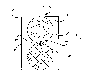
Fir~t turning to FIG. 1, an antenna radiating
system 10 i~ shown in a top view in FIG. l(a) and a ~ide
view in FIG. l(b). Radiating system 10 includes an
antenna element 12 for generating electro~agnetic waves,
generally at a mi~ e freguency. Antenna element 12
includes a dielectric substratQ 14, an upper conducting
patch 16 and a lower conducting patch 18. As is apparent
from the figures, upper conductive patch 16 is generally
circular in nature and is formed on a top portion of one
side of dielectric substrate 14. Conducting patch 18 is
Z393161
also generally circular in nature and is formed at a lower
portion of dielectric substrate 14 on an opposite side
from conductive patch 16. The conducting patches 16 and
18 are an appropriate conductive material, such as copper,
s and are adhered or printed to dielectric substrate 14 by
an applicable method such as vapor deposition or a rolling
process as are known in the art. The F~p9~ of conducting
patches 16 and 18 can be formed by an etch~nq process as
is also known in the art.
In this embodiment, the generally circular
conducting patche~ 16 and 18 are tangential to each other
with r~pect to the top view. r~w-ver~ by viewing the
side view of FIG. l(b) it is apparent that the spacing
between the bottom portion of conductive p~tch 16 and the
upper portion of ~Q~ ctive patch 18 for~s a slotline
portion through the dielectric substrate 14. Furthermore,
the arcuate shape of both con~l~cting patches 16 and 18
for~ a dual flared region at the slotline location
generally depicted by reference numeral 20. Consequently,
there are two region~ which fl~re inward~ towards the
center of the slotlinQ to form the dual flared slotline.
Conducting patches 16 and 18 are excited by a
coaxial feedline 22. CO~Y1A1 feedline 22 includes an
inner conductor 24 and an outer con~ctor 26, and a
connecting device 28 to connect coaxial feedline 22 to an
appropriate driving device (not shown). Inner conductor
24 transverses and i8 insulated fro~ the lower conducting
patch 18, and is electrically conr~cted to the upper
conducting patch 16, a~ ~hown. Outer conductor 26 is
electrically co.u e~ted to the lower con~l~ting patch 18,
as shown. Co ~eguently, a sinqle feedline 22 excites the
conductive patches 16 and 18 of antenna element 12. In
this manner, an appropriate, alternating excitation signal
at a desirable freguency applied to coaY~1 feedline 22
excites the conducting patches 16 and 18, which in turn
produces an electric field across the ~lotline region 20
209316:1
separating the two conducting patches 16 and 18. Because
the slotline region 20 i8 flared, the electric field will
be ~h~pe~ and have different electric ~ield strengths and
resist~es according to the distance between the
conductive patches 16 and 18. Also, other inputs, such as
mi~G~~rips, slotlines, coplanar wa~e~uides, and two- or
three-wire trans~ission line~ known to those skilled in
the art, would also be applicable.
The electric field across the slotline generates
radiating electromagnetic waves at a frequency set by the
parameters of the freguency of the input signal, the
dimension of the slotline and the size, shape and material
of the con~llcting patches 16 and 18. The ma~ority of the
generated waves propagate perpendicular to the plane of
lS the antenna element 12. The axi~ along the length of the
slotline determines at what orientation the electric field
will be relative to the propagation of the waves. For the
orientation of the slotline defined by ~o..~ ing patches
16 and 18 of the embodiment of ~IG. 1, the electric field
of the propagating waves will be oriented as shown,
perpendicular to the slotline in the plane of the paper.
Because the generatQd electro~agnetic waves
propagate substantially perpendicular to the plane of the
antenna element 12, it i~ generally desirable to provide
a ~o~A~lane which rQflects the portion of the
electromagnetic wave~ traveling in one direction in order
to rever~e its propagation direction, and thus enable
substantially all of the power ou~u~ of the antenna
radiating system 10 to be in one direction. This concept
is shown in FIG. 2, where a ~o~.~lane 30, shown in cross
section, is positioned relative to antenna element 12 by
appropriate means. The distance between the surface of
dielectric substrate 14 and the ~urface of ~o~l-d~lane 30
i~ selected to be a quarter-wavelength derivative of the
frequency of the generated waves in order to reflect the
waves in pha~e with the wave~ propagating from the other
2~93:~61
side of the antenna system 10, as ~hown. Consequently,
the majority of the electromagnetic intensity produced is
channeled in a ~ingle direction.
The antenna radiating system 10 discussed above
gives a number of desirable characteristics for use in a
multifunctional, low-profile radiating system which
includes wide bandwidth, ~mall ~ize, polarization
diversity and conformality. In addition, in certain radar
applications, system 10 should al o have low radar cross
section (RCS) characteristics in that it reduces the
probability that the system will be detected by radar.
Of all of the desirable characteristics mentioned
above, the most important feature for ~ost applications
would probably be in that sy~tem 10 exhibits excellent
impedance match~ng to the input signal and a wide
impedance bandwidth to free spacQ. This characteristic is
provided by the flared lotline being fed by a single
feeding device at the center of the slotline where the
slotline is the na~owe_~. This na~o~r~-~ dimension of
the slotline is selected to provide the desirable
impeA~ncs match~ng between the input line and the
slotline. In addition, the variable distancQ between the
two conducting patches 16 and 18 provided by the flared
slotline give~ a wide range of imFe~-ncs~ which enable the
electric field created acro~s the ~lotline to be matched
to the impeA~nce of free space.
The relatively small size of the different
conducting element~ and the thic~ness of the antenna
element 12 itself enables the radiating ~ystem 10 to be
easily implemented in many different multifunctional
systems, and to be -~pe~ to different structures, such as
curved surfaces. In one example, each of the conducting
patches 16 and 18 ha~ a diameter of approximately 0.325n.
The dielectric substrate 14 is positioned ~t approximately
0.25" from ~ro~ lane 30. Since the ~o~....... dplane 30,
substrate 14 and conducting patches 16 and 18 are
2~9316~
relatively very thin, the total thickness of the antenna
element 12 is also approximately 0.25", thus providing a
flexible structure to be shaped as desired. A system with
this dimen~ion performed well over 5-18 GHz with good
5 voltage standing wave ratio (VSWR) and radiation patterns.
The system as described above has its greatest
application in an arrayed configuration of antenna
elements. Now turning to FIG. 3, a top view of a
radiating system 32 including an array of antenna elements
10 34 is shown in a specialized configuration to demonstrate
the multifunctional capabllitie~. The array of antenna
element~ 34 are depicted in which preshaped metalized
patches on one side of a dielectric substrate and
preshaped metalized patches on the other side of the
15 dielectric ~ubstrate foml a plurality of consecutive dual
flared slotlines. Nore particularly, first preshaped
conductive patche6 40 on one side of a dielectric
substrate 36 are aligned with second prech~ped conductive
patches 42 on an oppo~ite side of the dielectric substrate
20 36 to for~ a series o~ dual flared slotlines represented
by regions 38. A8 i~ apparent, the edges of each
conductive patch 40 and 42 which are ad~acent on the
opposite sides of the dielectric substrate 36, are ~
in a wave-like fashion to form the slotline regions 38.
25 In thi~ embodiment, each of the conductive patches 40 and
42 are connected to a coAY~l feedline comprising an outer
conductor 44 and an inner conductor 46 proximate the
na~owc_l region of each slotline 38, a~ ~hown. As above,
each of the inner conductor~ 46 are connected to
30 conductive patches 42 and each of the outer conductors are
connected to co~ Gtive patche~ 40. Each of the coaxial
feedlines are driven separately at a common frequency and
selected phase to produce electromagnetic waves radiating
from system 32 with a coherent phase front. In array
35 system 32, the polarization is again aligned along the
orientation of the slotlines 38 ~uch that the
2093161
electromagnetic wave is polarized in the direction
perpendicular to the slotlines 38.
Now turning to FIG. 4, a radiating system 50
incorporating a second array of antenna elements 52 is
S shown. ~n this embodiment, the shapes of the different
conductive patches are more akin to those of the
conductive patches 16 and 18 of FIG. 1. More
particularly, the array of antenna elements 52 includes
three rows and three column~ of substantially circular
conductive patches in an alternating configuration where
conductive patches 56 on one side of a dielectric
substrate 54 alternate with conductive patches 58 on the
opposite side of dielectric ~ub~trate 54, as shown. In
other word~, a Co~ ctivQ patch on one side of the
substrate 54 will b4 ad~acent to conductive patches on the
opposite side of ~ubstrate 54. Con~equently, two columns
and rows of three commonly polarized dual flared slotlines
are formed, one of which i8 depicted by reference numeral
62. By incorporating coaYl~l fee~ng devices 60 at each
slotline location, as with FIG. 1, it is possible to
produce a ~ource of electro~agnetic radiation which is
polarized in two orthogonal directions. More
particularly, the slotlines which are ~ligned in the rows
will have a polarization in one direction and the
slotlines which are aligned in the columns will have a
polarization in a direction perpendicular to the
polarization of the other direction. Conseguently,
polarization diversity can be achieved for a wide variety
of applications.
The foregoing A~-r~-7ion discloses and describes
merely exemplary embodiment~ of the present invention.
One skilled in the art will readily reco~n~ze from such
discussion, and from the accompanying drawing~ and claims,
that various changes, ~odification~ and variations can be
made therein without departing from the spirit and scope
of the invention as defined by the following claims.