Note: Descriptions are shown in the official language in which they were submitted.
CA 02093635 2000-08-14
- 1 -
MAGNETRON SPUTTER COATING METHOD AND
APPARATUS WITH ROTATING MAGNET CATHODE
5 Field of the Invention
The present invention relates to
sputter coating and more particularly to
magnetron enhanced sputter coating processes
10 and apparatus employing magnets which are
movable with respect to a sputtering cathode
target.
Background of the Invention
15
Sputter coating is a process carried
out in a vacuum chamber which is filled with a
20
,r
W~ 92!07970 PCT/US91/07683
~a
s~' 936~5
rs ~fl
_ 2 _
generally cheanically inert gas in which a substrate
is coated with a material from a target of
sputtering material subjected to a negative
electrical potential with respect to the chamber.
wall or other anode. The potential gradient
adjacent the target surface causes electrons to be
emitted from the target which, on their way to the
chamber anode which is usually formed in part by
the grounded chamber wall, strike and ionize some
l0 of the inert gas. The positive ions formed are
. then. attracted to the negative target which they
strike, transferring momentum to the target
material, and ejecting particles of the material
from the target surface. The substrate to be
coated, which is positioned in the chamber usually
with its surface facing the target, receives some
of the ejected particles which adhere to and coat
the substrate surface.
With magnetron sputtering, a magnetic
field is farmed over the target surface, usually
including magnetic field lines parallel to the
target surface, and, in many applications, in the
form of a closed magnetic tunnel. The magnetic
field causes the electrons emitted to move in .,
curved spiral paths which trap them in regions
proximate the target surface enclosed by the field,
thereby increasing the rate of electron collisions
CA 02093635 2000-08-14
- 3 -
5 with gas atoms, which in turn increase the
ionization of the gas and the efficiency of
the sputtering process.
In applicant's U.S. Patent No.
4,957,605, issued September 18, 1990, a
10 sputter coating apparatus and method are
disclosed in which a concave annular target is
provided with concentric annular
electro_~agnets which cause the formation of a
pair of concentric plasma rings. The plasma
15 rings are alternately energized by alternately
supplying current to energize the magnet coils
while the target power level is switched in
synchronization with the switching of the
current to the magnetic coils. This causes
20 different rates of sputtering from inner and
outer concentric regions of the target
surface, with the sputtering from each region
causing different distribution characteristics
of the sputtered material deposited on the
25 substrate or wafer being coated. Varying the
relative parameters affecting the energization
of the two target regions provides control of.
coating uniformity on the substrate surfaces,
which is especially important on the
30 differently facing surfaces of stepped
CA 02093635 2000-08-14
- 4 -
5 semiconductor wafers. The aforereferenced
patent particularly describes effects on the
coating caused by the target geometry and by
the electrical parameters relating to the
energization of the target and plasmas.
10 In magnetron sputter coating
processes, the sputtering of materials from
the sputtering target occurs most rapidly into
regions of the target where the plasma trapped
by the :magnetic field is the most dense. This
15 causes the proportionate consumption or
erosion of the sputtering material from the
target surface. The erosion of sputtering
material from other portions of the sputtering
target surface generally occurs at a rate
20 which varies in proportion to the strength
and/or duration of the plasma over that
portion of the target surface.
In the prior art it has been
proposed in certain applications to move the
25 magnetic field in relation to the sputtering
target surface either by movement of the
target or movement of the magnetic field. A
purpose of the relative movement of the target
or magnetic field with respect to each other
30 is, in many cases, to provide a more uniform
erosion or consumption of the sputtering
target
t.;i
iii..
i;~. i
W~ 92!07970 PCT/US91/07683 ,
~2~93
material over the surface of the target. Such
devices have for many reasons been unsatisfactory.
In sputtering from a sputtering target
while moving the target with respect to the
magnetic field, a desirable erosion pattern is
sometimes achieved for purposes of uniformly
consuming the target material, but often such a
pattern does not provide the proper or desired
distribution of sputter coating material onto the
surface of the substrate being coated.
Furthermore, such devices of the prior art have
insufficiently controlled the distribution of the
plasma or the duration of the moving plasma with
respect to the target surface so as to affect a
desired non-uniform erosion pattern.
In addition, rotating magnet devices of
the prior art have not effectively provided for the
sputtering of the entire surface of the target. It
has been found that the absence of at least some
sputtering from any given region of the target may
cause redeposition.of the material sputtering from
elsewhere on the target onto those regions where no
sputtering is occurring. This causes a build-up of
.'..:,. sputtering material which is undesirable.
Accordingly, there is a need to provide a
method and apparatus for sputter coating substrates
which employs a magnet which is movable relative to
r 9~'~ 92/07970 PGT/~JS91/07683
..
zu~ ~~3~
:, _6_
the sputtering target and which is capable of
precisely controlling the distribution of
sputtering on the target surface in its entirety. .
When the magnet structure and target are
rotated relative to each other, the prior art
devices have failed to provide for sufficient
sputtering from certain regions of the target
surface, such as the center and edge regions of the
target, and further have failed to effectively
distribute the sputtering across the target surface
in a manner which is effective to produce the
desired erosion pattern to yield the proper coating
uniformity on the substrate.
Summary of the Invention
;,.,
Tt is an objective of the present
invention to provide a sputtering coating method
and apparatus in which a magnet, positioned behind
a sputtering target opposite the sputtering surface
to generate a plasma trapping closed magnetic field
or tunnel over the sputtering target surface, is
shaped and rotated so as to produce a desired
average sputtering distribution across the surface
of the target.
xt is a more particular objective of the ,
present invention to provide a rotating magnet
magnetron sputtering apparatus that avoids
unsputtered areas of the target, and thus avoids a
6
.., ., ,.i ,. " .,~.~ . ~,...;.... ..,.~;-..'~.. . , ~~ .
:~e:
'~i W~ 92107970 P~f/US91/076~~
::; ,:r,,' 3~3~
_~_
buildup by redeposition of sputtered material on
the target.
It is another objective of the present
invention to provide a rotating magnet sputtering
target apparatus and method having a magnet
structure which is configurable to produce a
desired coating deposition on the substrate when
the magnet structure is rotated during sputtering.
It~is a further objective of the present
invention to provide the rotating magnet structure
in a sputter coating apparatus wherein the rotating
magnet structure facilitates the circulation of
cooling fluid for the sputtering cathode assembly.
According to the principles of the
present invention there is provided a sputter
coating apparatus having a sputtering target
' included in a cathode assembly with a magnet
located behind the sputtering target so as to
produce a closed magnetic field over the target
surface. The magnet is rotatably mounted so as to
rotate the magnetic field over the surface of the
sputtering target. The magnet is configured with
' respect to the target to cause sputtering from the w
,, center of the target to the outer rim of the target
at a rate which varies with the radius from the
center in a desired manner.
dV0 92/07970 PCTJiJS91/07683
y0936'~~
In the preferred and illustrated
embodiment of the present invention, the magnet is
preferably a permanent magnet which includes a ,
closed loop of magnetic material formed of a
flexible magnetic strip. The strip has its poles
spaced transversely across the strip, preferably
generally in the plane in which the closed loop
lies. The magnet, which is formed of flexible ,
laminated strips of magnet impregnated plastic, is
arranged on a rotating plate behind the sputtering
target in a shape having a plurality of curves
including a plurality of outwardly convex curves,
some near the outer rim of the target, and at least
one point at which the strip passes near, but not .
through, the target center. The magnet is shaped
in such a way that the plasma trapped by the
magnetic field will be present over various
portions of the sputtering target at various radii
from the center for predetermined amounts of time
so as to provide a desired erosion pattern on the . '
target surface.
According to the preferred embodiment of
the present invention, the magnet is polarized in
such a way that one pole faces the outer edge of ,
the rotating plate while the other pole faces the
axis of rotation so that, particularly at the outer
edge, the field emerges from the magnet and
~J
~S
;gym W~ 92/0797 , , PCT/U~9i/07683
.
;~u .;a~'~~
'
,. , r.
'- 9
;i;,. 2093a3~
surrounds the outer rim of the target to facilitate
sputtering from the target rim, without the need to
provide an enlarged magnet structure extending
beyond the target outer rim.
In addition, according to a preferred
embodiment of the present invention, fixed lumped
magnets of different magnetic material are
positioned at various points along the magnetic
loop so as to selectively influence portions of the
1p magnetic field to provide certain desired field
shapes. Particularly, according to certain
preferred embodiments of the present invention, the
lumped magnets are oriented with one pole toward
the~target and one away from the target so that the
magnetic fields produced by the lumped magnets
cooperate with the field provided by the magnetic
loop to sharpen the field at various points.
Particularly, certain of the lumped magnets are
provided opposite the axis of rotation from the
point of the loop where the magnet most closely
approaches the axis. In this way, a small portion
of the magnetic field, which does not otherwise ,
extend across the central portion of the target, is
drawn across the center to provide some degree of
erosion to, and sputtering from, the central
portion of the target. In addition, in accordance
with certain embodiments of the present invention,
:%$q
WO 92/07970 PCT/U~91/07683
.>rt
'~~
2~936
.
z
_ 1~ _
the lumped magnets are provided at the outermost
reaches of the loop near the edge of the target to
shape the field more precisely in these regions. .,.'.
In accordance with further objectives of
the presewt invention, the target itself is shaped
in a way to cooperate with the sputtering pattern
,.. created by the magnetic configuration so as to
provide for a maximum utilization of the target
material. In this respect, the target is of non-
uniform thickness and is, for example, in the
illustrated embodiment, more particularly thicker
at the outer regions near the outer edge thereof.
In alternative embodiments, particularly
where there may be some advantage to varying or
adjusting the magnetic field strength, any of the
magnets, and particularly the closed loop magnet,
may be electromagnets.
In acco~:dance with further objectives of
the present invention, the target is banded or
otherwise secured in intimate heat conducting
contact with a target nest. A closed cavity is
provided behind the target nest enclosing the
rotating magnet. A turbulent layer of water or
other cooling fluid is maintained by injecting ,
cooling water into the cavity behind the nest. The'
fluid is injected into the space near the center of
the target assembly near the axis of rotation of
,,:,
W~ 92/07970 PCT/'US91/07~~3
2~~3~~3
- 1 1~ -
' the magnet so as to flow through a narrow space
between the rotating magnet and the back surface of
the target nest. In this space, the cooling fluid
is propelled along the back surface of the nest and
outwardly by the rotation of the magnet structure,
and more particularly by the raised surface of the
magnets themselves, so as to provide a turbulent ,
skin of cooling water adjacent the surface of the
nest improving the flow of the water and the
cooling effect thereof.
These and other objectives and advantages
of the present invention will be more readily
apparent from the following detailed description'of
the drawings in which:
Brief Description ~f the Drawings
Fig. 1 is a cross-sectional view through ,
a target assembly of one preferred embodiment of an
apparatus embodying principles of the present
invention.
Fig. 2 is a view taken generally along
lines 2-2 of Fig. 1 illustrating the face of the
rotatabl~ plate and magnet assembly.
Fig. 3 is a cross-sectional view along
lines 3-3 of Fig. 2.
Fig. 4 is a fragmentary cross-sectional
view along lines 4-4 of Fig. 2.
CA 02093635 2000-08-14
- 12 -
5 Fig. 5, is a view similar to Fig. 2
illustrating an alternative rotating magnet
assembly configuration.
Fig. 6 is a set of diagrams A
through D illustrating the preferred magnetic
10 pole orientation for the main magnet according
to certain features of the present invention.
Fig. 7 is a set of diagrams A
through D illustrating a preferred auxiliary
magnetic arrangement according to certain
15 features of the present invention.
Fig. 8 is a set of diagrams A and B
illustrating a preferred auxiliary magnetic
arrangement according to other features of the
present invention.
20 Detailed Description of Drawings
Magnetron sputtering devices of the
type to which the present invention relates
are described in applicant's U.S. Patent Nos.
4,909,695 and 4,915,564 both entitled "Method
25 and Apparatus for Handling and Processing
Wafer-Like Materials", issued March 20, 1990
and April 10, 1990, respectively; and,
U.S. Patent
,~;,~
WHO 92/07970
1'CT/US91/07683
- . .
' ~ r I~
'
'S . ,
i, .
i y~.'~
t
13 -
' No. 4,957,605, entitled "Method and Apparatus for
Sputter Coating Stepped Wafers."
w Fig. 1 illustrates, in cross-section, a
sputter coating processing chamber 10 of a sputter
coating apparatus according to principles of the
r present invention. The chamber 10 is a portion of
the sputter processing apparatus disclosed in U.S.
Patent 4,909,695. The processing chamber 10 is a
vacuum processing chamber formed of an isolated
section of a main chamber 11. The main chamber 11
is isolated from the atmosphere of the machine
environment 12 by a plenum wall 14. The processing
chamber 10 is capable of communicating with the
main chamber 11 throughout opening 15 (shown
sealed) in the plenum wall 14.
As more fully described in U.S. Patent
4,909,695, the sealing of the opening 15 isolates
the chamber 10 from the main processing chamber 11
by the selective movement of a processing chamber
backplane section 16 against a portion of a disk
shaped rotary wafer transport member 17 clamping
the transport member 17 between the backplane
section 16 and the plenum wall 14 in a sealing
relationship (as shown), thereby enclosing a
backplane space 19 within the processing chamber 10
:<;
and isolating the processing chamber 10 from the
main chamber 11.
.... :~Y ..
?F;S
.a Vd0 92/07970 PCf/IJS91/076~3
6~p936'~~ ~r'~~, . .
_ 14
Opposite the backplane section 16, on the
front plane side of the transport member 17, the
processing chamber 10 is isolated from the machine
environment 12 with a cathode assembly module 20
mounted in a vacuum sealing relationship against
the plenum wall 14 surround the opening 15. The
module 20, or processing chamber frontplane
section, cooperates with the backplane section 16
and the transport member 17 to form the sealed
isolated processing chamber which is isolated from
both the main chamber 11 and the machine external
environment 12.
Within the processing chamber 10 is a
substrate or workpiece 27. in the form of a flat
silican wafer or disk which has the surface 22 upon
which a coating is to be deposited in a sputter
- coating process to be performed within the
processing chamber l0. ~L'he wafer 21 is held by a
. set of clips or other retaining devices 24 in a
wafer holder 25 resiliently carried by the
transport member 17. The transport member 17 is
rotatable within the main chamber to bring the
holder 25, and the workpiece or wafer 21 into
alignment with the hole 15 so that the processing
. 25 chamber 10 can be formed around the wafer 21 on the
holder 25 by transverse movement of the backplane
section 16 to move the member 17 against the plenum
CA 02093635 2000-08-14
- 15 -
5 wall 14. The transport member portion 17 is a
transversely movable ring carried by a
rotatable index plate which is not shown, but
described more fully in the above patents Nos.
4, 909, 695 and 4, 915, 564.
10 In this preferred embodiment, the
wafer 21 is supported in a plane perpendicular
to, and concentric with, a central axis 27 of
the main chamber 10, which is also concentric
with the hole 15 in the plenum wall 14.
15 Surrounding the wafer 21 on the holder 25 is a
disk 29 which at least partially protects the
holder 25 from an excessive accumulation of
coating intended for but which missed, the
surface 22 of the wafer 21. Details of the
20 sputtering apparatus of which the processing
chamber 10 is a part including particularly
details of the wafer transport 17, wafer
holder 25, and backplane section 16, are
described and illustrated in U.S. Patent
25 4,909,695 and 4,915,564.
The cathode assembly module 20
includes two assemblies, a removable cathode
assembly 30 and a fixed assembly portion 31.
The fixed assembly portion 31 is an annular
30 enclosure rigidly mounted in sealed
relationship against the plenum wall 14
surrounding the opening 15. It includes a
cylindrical metal side wall 33 of the chamber
10,
VNO 92/07970 PCT/'tJ~91/076~3
209363 - 16 -
which is electrically grounded to the frame 14 of
the plenum, a wafer holder shield 34 which
surrounds the opening 15 and a chamber door frame
assembly 35.
~ The cathode assembly 30 is mounted to a
hinged door assembly 37 which removably but
sealably supports the cathode assembly 30 to the
fixed assembly 31. The cathode assembly 30 carries
the sputtering target 40, which is a circular
target having a continuous smooth concave
sputtering surface 41 and,a back surface 39. The
assembly 30 supports the target 40 with its axis in
alignment with the axis 27 of the chamber 10 and '
with its sputtering surface 41 facing the surface
22 of the wafer 21 to be coated.
The target 40 is supported in a target
~~est 42 having a front surface 43 conforming to
surface 39 and concentric with axis 27. The back
surface 39 of the target 40 is soldered or
otherwise bonded to the front surface 43 of the
nest 42, in intimate thermal contact therewith.
The target back surface 39 is a cooling surface
which, when the target 40 is mounted in holder 42,
conforms to and lies in close Gaoling contact with ,
the surface 43 of the holder 42. Behind the nest
' 42, opposite the cooling surface 43 thereof, is a
space 44 for the circulation of cooling liquid,
yr~ f6~0 92/07970 " PCT/US91/07683
°' ~ 2~'~~~3~~
~.Tw:
?a tr
i ;
::~.:: . ~.. n
which is generally water, to remove heat generated
in the target 40 during sputtering by cooling the
heat conductive target holder 42. The cooling
fluid is circulated into and out of the space 44
from an inlet port 45 to an outlet port 46 in a
magnet assembly 50, as described below. The space
44 is enclosed behind the nest 42 by a housing
structure 48 onto which the nest 42 is rigidly
supported, and to which it is secured by bolts 49.
ZO The shapes of the surfaces of the target
40 are preferably such that all the target 40 is
v capable of being formed by turning block of
sputtering material on a lathe. The target holder
40 is made of a heat conductive and electrically
conductive material, preferably hard tempered OFHC
copper or Alloy 110.
_s
The magnet assembly f0 includes a shaft
51 having a threaded end 52 by which the shaft 51
is rigidly mounted in a threaded bore 53 at the
center of the back surface of the nest 42. The
assembly 50 also includes a rotatable magnet ...
carrier assembly 55 which includes a circular disk
56 of non-magnetic stainless steel or other such
material having a central hole 57 therein at which
,
the disk 56 is rigidly mounted to a sleeve assembly
58 rotatably mounted through a bearing assembly 59
through the housing 48 and to the nest 42 to rotate
a
WO 92/0797~D P~'/T.JS91/07683
.'a _ 18
about the shaft 51 on the axis 27. The rotatable
magnet assembly further includes a magnet structure
60 rigidly mounted on the disk 56 to rotate '
therewith. The magnet 60 surro2inds the axis 27 and
lies beneath or behind the nest 42, opposite the
front surface 43 thereof, and close enough thereto
to generate a closed magnetic field above the
sputtering surface 41 of the target 40 mounted on
the surface 43 of the-nest 42.
The shaft 51 has a cooling fluid inlet
- duct 62 extending therethrough which communicates
' with the inlet port 45 to the interior cooling
chamber 44 between the nest 42 and the housing 48.
The housing 48 has mounted near the edge thereof a
cooling fluid outlet duct 63 which communicates
with the fluid outlet port 46 in the cooling space
44.
Mounted to the back of the housing 48 is
a bracket 64 to which is mounted a magnet rotary
drive motor 65. The motor 65 has an output shaft
66 with a cogged drive wheel 67 mounted at the end
thereof for driving a cogged drive belt 68. The
belt 68 extends around a cogged drive wheel 69
attached to a drive shaft 70 which is rotatably
mounted on the housing 48 extending therethrough
and having a free end 71 to which is mounted a
drive gear 72. The drive gear 72 is positioned
VV~ 92/07970 PCT/US91/07683
'1
'~ 2~93~3~
- 19 -
within the space 44 where it engages a mating gear
74 attached to the disk 56 of the rotatable magnet
assembly 55. Accordingly, the motor 65, when
energized, rotates the magnet assembly 55 to rotate
the magnet 60 behind the target nest 42 to rotate
the magnetic field over the sputtering surface 41
of the target 40. The details of the construction
of the magnet structure 60 and its arrangement on
the magnet assembly 55 can be better understood by
reference to Figs. 2-4.
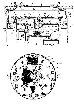
Referring to Fig. 2, according to one
preferred embodiment of the present invention, the
magnet structure 60 is shown supported on the disk
or plate 56. The magnet structure 60 is a strip of
flexible magnet impregnated plastic made up of a
laminated plurality of flexible plastic magnetic
ribbons 80, for example 24 in number, arranged in a
closed irregular loop on the plate 56. The shape
of the magnet 80 is selected such that, as the
magnet rotates, the strength and duration of the
plasma at any given radius of the target will cause
sputtering at a predetermined desired average rate
necessary to produce a desired coating distribution
an the target. The thickness of the target 40 is
further varied across the radius of the target to
supply material in proportion to the demands of the
sputtering distribution.
i~1'O 92/07970 PC'f/TJS91/07583
,' -- 2 0 -
The ribbon magnet 80 is held in place in
a particular predetermined shape surwounding axis
27 by five clamping blocks 81--85. The ribbons of
the magnet 80 are polarized in such a way that one
pole of the magnet formed thereby faces outwardly
toward the outer rim 87 of the disk 56 and toward
:;
the clamping blocks 81, 83, 84 and 85, while the
. other pole faces inwardly toward the clamping block
82. In the particular embodiment illustrated, each
l0 of the ribbons has its north pole facing inwardly
and its south pole facing outwardly.
Mounted to the clamping block 82 and
positioned about the central axis 27 are three
permanent magnets 90, 91 and 92 which are held to
the block 82 by clamps 94. Each of the magnets 90,
91 and 92 is oriented with its north pole facing in
the general direction toward the target nest with
its south pole facing generally toward the plate
56. In the particular embodiment illustrated, the
north pole of magnet 90 is inclined at an angle of
appraximately 45 degrees toward the central axis 27
while the magnets 91 and 92 are oriented parallel
to the axis 27.
In Fig. 5, an alternative embodiment of. ,
magnet structure 60a is illustrated which is
differently shaped than the magnet 60 of the
embodiment of Fig, 2. The ribbon magnet 80a of the
i
.r
,
9W0 92/07970
~ ~ ~ ~ ~ ~
~ ~'lTJS91/07683
,:"~;~
,._
!
4
; 21 a
magnet structure 60a is secured to the disk 56
through appropriately shaped clamping blocks 81a-
85a. In this embodiment there is also provided
additional permanent magnets 95,.96, 97 and 98
clamped 'to the block 82a by clamps 99 and oriented
with their north poles facing towards the target
and nest, their south poles toward the plate 56 and
their axes generally parallel to the axis 27 of the
cathode assembly.
The magnets are arranged on the carrier
plate 56 to cause sputtering from the target 40 to
be distributed in such a way as to achieve a
desired distribution, usually a uniform
distribution, of the coating material on the
substrate 20. With a generally circular target 40
and circular substrate 20, with a magnet assembly
that rotates about the axis 27 through the centers
of the target ~0 and substrate 20, as in the
illustrated embodiments, the relative average
sputtering rate will be constant at any given
radius from the target center, but may vary with
the distance from the axis 27. The variation will
be a function of the average intensity of ion
bombardment of the target surface at any given
radius, which is in turn a function of the average
plasma density aver the area of the target at that
the given radius. This variation will generally be
y.
::r
s dV~ 92/07970 P(.'T/US91/07683
;:1
22
proportional to the portion of a circle at any
given radius which is enclosed by the. magnetic
field. Integrating the plasma density around such ,
circles will yield the approximate relative
sputtering from the target surface 41 at the given
radius from the target center.
To obtain erosion of all parts of the
target, it is necessary that the plasma be present
for some portion of the rotation of the magnet
assembly over every region of the target. This is
desirable even over regions where sputtering of
material from the target is not necessary, since
the total lack of ion bombardment of the target
surface at any point usually results in a
redeposition of sputtering material. This most
often occurs at the edges and center of the target.
The difficulty in producing the magnetic field
close to the target edge i~~ due in some
circumstances to the undesirability in enlarging
the cathode assembly to include a large diameter
magnet, particularly with a rotating magnet. With
a rotating magnet, the presence of the magnet at
the axis of rotation causes excessive sputtering at
the center, since the magnet will not rotate ,
through the center of the target.
As illustrated in Fig. 6, the properties
of one of the features of the present invention is
VV~ 92/07970
PCT/gJ~91/07683
'~ 2~9~3~3a
~~i~ 23 .
presented in a series of diagrams A through D. In
diagram A of Fig, 6, a magnet arrangement is
illustrated wherein a pair of magnets 101 and 102
';v
are spaced opposite a gap 103 on a steel carrier
104 to produce a magnetic field 105 over the target
.; 106. The lines of the field 105 generally emerge
from the surface 107 of the target 106
approximately perpendicular to the surface and
immediately above the magnets 101 and 102. Unless
l0 the magnet structure is enlarged with respect to
the target 106, this often results in a region 109
adjacent the edge 110 of the target 106 that is too
remote from the plasma trapped by the field 105 to
receive a bombardment of ions to cause sputtering.
As a result, sputtering material may be redeposited
on the region 109 of the target 106, as illustrated
by the erosion profile 111 in diagram B of Fig. 6.
As illustrated in diagram C of Fig. 6, in
accordance with one of the features of the present
invention, t-he magnet 80 is oriented on the carrier
plate 56 with the poles spaced parallel to the
target so that the field lines 112 emerge from and
reenter the magnet 8o with a component which is
angled along the radius of the target 40, most
importantly in a direction away from the center and
encircling the target edge 115. as a result, a
portion of the plasma is sufficiently close to the
'3i~
i.~
ffO 92/079711 PCT/US91/076$3
4:.
;:, 2(~936~~
- 24 -
edge to cause enough sputtering from the region
near the edge of the target 40 to prevent an
accumulation of redeposited sputtered material, and
to sputter any additional material from the edge as
' 5 may be desired. As a result, the eroded profile of
the target is in accordance with that shown at 116
in diagram D of Fig. 6.
Producing a desired sputtering rate at
the center of the target, according to other
features of the present invention, is illustrated
in the diagrams of Fig. 7. Referring to diagram A
of Fig. 7, the field from the main magnet 80,~at
its point proximate the center of the target 40, is
illustrated in diagram A of Fig. 7. There it is
necessary that the field portion 120 be
sufficiently spaced from the center axis 27 of the
target 40 to prevent excessive erosion and burn-
through of the target 40 at the center. As a
result, little sputtering occurs at the target
center and, accordingly, there is a tendency for
sputtered material to redeposit and build up at the
target center. The provision .of the auxiliary
magnets 90, 91 and 92, around the axis 27, with
their poles oriented so that their fields combine ,
with that of 'the magnet 80 to produce a resultant
,. field 118, draws sufficient plasma over the target
center to cause the redeposited material at the
.:i.Y~ .
..:.: ~.;~
W~ 9Z/07970 . - - PCT/US91/07683
' :,<~ ,
T..
.. - 2 5 _~
target center to be resputtered from the target,
and, in addition, for any other material of the
target at the center to be sputtered, without
excessive sputtering to occur at the target center,
as illustrated by the erosion profile 122 in
diagram D of Fig. 7.
Auxiliary magnets such as the magnets 95-
98 in Fig. 5, according to other features of the
present invention, cooperate with the main magnet '
80a of Fig. 5, to sharpen and reshape the field to
redistribute the erosion of the target. As
illustrated in diagram A of Fig. 8, the field 130
of the magnet 80a may, for example, cause excessive
sputtering along one edge, for example the inner
edge, of the magnetic tunnel. By provision of the
auxiliary magnet 95, for example, as illustrated in
diagram B of Fig. 8, the z~esultant field 131 is
reshaped to better achieve the erosion and
sputtering distribution characteristics desired.
The magnets 80 and 80a are dimensioned so
as to project a slight distance, approximately 1/32
inch, into the space 44 between the back of the
target nest and the carrier 56, leaving a clearance
',:, , between the magnet of, for example 1/16 inch
bettaeen the magnet and the nest back and about 3/32
inch between the magnet retaining blocks 81-84 and
81a-84a and the nest back. The :.~.agnets 80, 80a,
Y
W~ 92/0797U PCT/U591/07683
.si; ~ n ~A
~'.;h
36~~
- 26
because of their serpentine shape, thus turbulently
move the cooling water through the space 44 as the
. magnet assembly 50 rotates. This causes the water
or other cooling liquid being used to more
effectively remove heat from the nest 42 and to
facilitate circulation of the water from the
central portion toward the outer portion of the
space 44 by a centrifugal pumping action, as shown
by the arraw 140 in Fig. 1. With this feature, the
l0 apparatus may be oriented with the substrate
horizontal, but if in a vertical plane, is
preferably with oriented upward direction being the
direction of the arrow 142 in F'ig. 1, and with the
cooling water outlet 63 at the top or high point in
the space 44.
Having described the invention in its
~Sreferred embodiments, the following is claimed: