Note: Descriptions are shown in the official language in which they were submitted.
372~
Optical Communicatior~ Syst~m w;th a Power
lirr,itcr for High-~nergy Pulses
The pres~rt inv~tion re!ates to an opticaL communica-
tion system as sc~t forth in the preamble of claim 1.
Such system~ are known, e.g., frc,m a. Wedding et al,
"10 Gbit!s to 260000 Sub,cribers Using Optical Amplifier
D;str;bu.ion Net,~ork", Contribution for ICC/Supe~comm
'9~, Opti~a~ Commurlicatic)ns 300 Level Session, "Impact
o~ Opt;cal Am~liFiers or, ~etwork Architectures".
In such ofticdl comrnunication systems, ;n which the trans-
mission llnk is ~ fiber-optic link, optical amplifiers
serve to a.~plify optical iignals transmitted through
the Optical wave~3uides.
The opti~a' amplifier chosen ;n the embodiment described
below ;5 a fiber-optic amp'ifier. A fiber-opt;c ampl;-
fier -is s~o~n in EP O 457 34~ A2, for examPle.
In such fiber-opi~ic amplifiers, erb;urn ions with which
a sect;on .~f optical waveguide is doped are raised from
a ground s tate to an exc ited state by pump light
em;tted b~ a pumf) sourcc~ and from the excited state,
the ions drop back, throlgh e;ther spontaneous or stimu-
lated emissiorl, to th~ ground state. The st;m~lated emis-
sion is e~ited oy the optical signal to be amplified,
~3~
whirh tra~els thtowgh the section of doped optical wave-
gu;rle. Th ~pont~neou~; emiss;on is also amplif;ed ;n
the doped ~;ection o~ opt-ical ~aveguide; this amplified
spontaneou ~mi~ion (A5~) causes the noise internal
to a fiber-opti(: amplifie~
In the ab~e-menlionec' syste~, there is the danger that
;n the ev~,;t of a break -in the fiber-optic l;nk,
e.g., du~ tc fit,er br~ak3~e or to separat;on of a f;be~-
optic con-,e~t~r, s~stem components, such as pho~od;odes,
will be da!naged.
This carl l~? eYplained as foLlo~s:
As a re~u~ of the break ;n the fiber-optic link,
the powe~ input to the op~ical amplifier decrea~es to
zero. Since the pumping process ;s independent of the power
input, er,ergy will be pumped ;nto the dooed oDt;cal-waveouide
section even if the power ;nput has dropped, so th~t com-
plete populc,t;on ;nversion w;ll occur. When light
which re~ul~s from sp-)ntaneous emiss;on and is reflect-
ed at thc interf~ce o~ the break in the fiber-
opt;c l1n~ i)asse~ ~hro~lgh the section of doped optical
wave~uide,whose active l~ser medium, e.g., erb;um ;ons,
;s ;n the -invert~d stat~, the stored enerc~y will be
suddenly re~eas~d. High energy pulses w;ll be emitted
which are a danyer to s~stem components.
These g;ant pul~es oropagate both in and opposite to the
direct;ol, Df signal tlow. In the case of erb;um-doped
fiber-optic ampl;fiers, the wavelength of the gi~nt
pulses is ~n the range between 15Z0 nm and 1570 nm.
_ 3 _ ;~372~
Such fit)el~-()ptic a~plifi~rs are not only used in optical
communica~ion ~stems~ ine~ are also employed in assem-
blies ~1 Iro~isional setu~)s which are provided for the
start-up ~J~ s~ch s~stems to permit measurements, tests,
or step~ st~p installation. Reflecting surfaces may be
intention,.lly or u~inten~ionally inse~ted in these set-
ups and mil~ tnen cause back reflection of the light
amplificd ~, the amplifier. Such reflecting surfaces
are formei~ ln particular by a connect;ng element or a cut-
off end of t1n optical waveguide.
An optica~ ampli~ier witl, a section of doped optical
waveeu;de mây h.lve such a high gain that, if subjected,
for exam~.!e, to unintentional back reflection, it will
turn into 3 Lase~ GSCi llator due to a phenomenon called
"Q-switchlr;y". ~hiC, too~ ~uses hi~h-energy pulses
wh;ch nldy ~anlaQe system components. A known solution to
the probl-r~ of how to avoid such daraage consists of
insertin3 or,e or more op~ical isolators in the optical
transmissicn path. These isolators can transmit l;ght ;n
only one direction, whereby back reflect;ons are prevent-
ed. Thus, t~,e optical amplifier can be prevented from
operatin~ as a laser oscil~ator. OPtical isolators are
the p~ssi e components with the highest complexity and,
thus, the ri~hest price in a system or an optical ampli-
fier with GptiCa l waveguide.
It is the o~ject of the in~ention to prov;de an optical
communic~;ior~ ~yst~m co~r;sing optical amplifiers where-
in th~ da~;~er of s,stem comPonents being damaged by high-
energ~ ~u~ies i~ a~oided.
~37~l~
Th;s Oi~ je~:L i.~ a~.tainr:(i as set forth i.n claim 1 Further
advantar~r~ous as~ct-s of ~he invention are defined in
the subclainl~.
The in~rltion will no~. be explaineci in rnore detail with
reference tc the accompar\ying d~w;ngs, in which:
fig 1 sr;J~S on~ r-mbodin~ent ~f an optical cr~mmuni-
ca~;on system wi~h power ~imiters in accor-
d;,~ce wi~:h the invent;on,
Fig~ ~ lr:Oh'S th.~ attenuation of a power limiter
as a f~n~;tion of the optical power input
to the l,m;ter, c~nc-i
Fig. 3 slow~ a riber-optic amplifier ~ith a oower
lim;ter for ar, optical communication sys-
t e m .
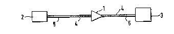
Fig. 1 sho~s an optical colnmunication system with an elec-
trical-to-optical. ~ransduGer ~ at the transmitting end
and one ol:.t.ical-!:o-ei~eç.trical transducer 3 at the re-
ceiving er,l, which ar~ interconnected by an optical
~iaveguide 5. A colnmunicaiic)n system ~iith an electrical-
tO-OptiCd trans~iucer at the transmitt;ng end and two
or more ci~tribuied optir:al-to-electr;cal transducers at
the receivir-g end ;s also ~ossible. This is of no con-
sequence t or' tile invention
The commuricatioa ~ystem of Fig 1 f~rther includes a
fiber-opt c amPlifier 1 and two power l;miters 4.
- s- 2~372~
In this e~bodimeilt, as scer~ in the direction of propa-
gat;on uf the oprical sigl13l, one power limiter 4 is
~ ted 1~ead ol the ~ibel-o~tic amplifier an~ one be-
hind the .~mplifiar~ and they ~re implemented as sec-
tions of (1 ped optic~l wa~egu;de. The two power (imiters
are joine(~ to the fiber-~p~;c ampl;fier 1 and the optical
wav~guide i ~-sin~ conventional splicin~ tethn;ques.
The power limitels ma~ also be imple~ented differentLy,
e.g., as ~idtPle.s of abcjc,rb;ng mater;al which are in-
serted i" the signal path at breaks
in the Opticdl h'3Ve~Uide, e.g., in front of and behind
the opt;c-" amplif;er, respectivelyA
Th;s abs"rbing matericll has p~operties wl1ich are de-
srribed bll~w
It is a~s~ po~3ible to place one power limiter behind
the electricaL-t~-opt-ical transducer ~ and one in front
of the op;ical-to-electr;cal transducer 3. This pro-
tects thes~ system components from the effects of
giant pul~es.
In pr3cti(al use, ~ibPr-,~pt;c amplifiers are also
arransed n cascide. ]n that case, each of the links
between the ;ndi~inual ~iber-optic amplifiers may con-
tain one ~!ower limiter.
The power limiter has the following properties.
The po~er ~imit~r passes the optica~ signal with a normal
' : .'
~ 6 ~ 372~
optical ~ wl~r (a few !O nw~ and a wavelength of, e.g.,
~ 15SO rm nearly unattenlJated. ~y contrast, it
stron~ly atter\ucl'-e~; opti~al powers which correspond to
that cf ti ~? gi3nt pulse ~watt ranye).
This is illustrated in ~i~. 2. The power ratio
T = PtL~
Po
is plo~te(, dS d fur;ction of the optical power input P~
to the ~ow~ iter. P(~) is the optical power output
of a powe~ limiter of length L.
The depen{ierlce of the attenuation in the power li~iter
is prefcrally nolline3r~ as shown in F;g. 2, so that
high-power opt;cal ra~-Jiation w;ll be attenuated d;s-
proportionately.
This ~tt~n~atior\ in the power lim;ter can be providedby ~;ght (attering. and/or absorption. The power li~;ter
is preferai~ly ma~e of an absorbing material in which
the absor~;tion i~ a two-~hoton process. The latter
exhibits ;he part;cularly suitable nonlinear dependence
of the op'ical input power. Th;s absorption is de-
scribed, 10r exa~ple, in a book by r~R. Shen, "The
Principle: ~f Nonlinear optics", John Wiley ~ Sons,
pp. 202-2 ~), but nct in connection with a particular
matarial r(ld not in connection ~;th optical waveguides.
The aforelknt;o~ rec~uiremc?ntS are fulfiLled, for
examp~e, '~ a s~ction of doped optical waveguide made
~3~2~
of an abio!~,irlg n~aterial with two-photon absorpti~n.
Such an diJsort~ g mat~rial is neodymium~ Nd, or
thu~i~;m, ''m, fo~ e~ample.
i~y an app!ot~riate cholce of the dop~nt and the doping
concentra!;on in an optical waveguide, two-photon ab-
sorl~tion is caused. The attenuation of the power
limi~er i~, determ;ned by the length of the section of doped
optical wavregui~.
~he fiber-o~tic amplifier ~iven as an example in ~i~. 3
tomprise. Lae fo'lo~ g elements, whose operation is
~nown from the alove-cited literature:
-- A st?ct i~ n of daped optical waveguide 33, wh;ch i5
doped wit~, e g , erbium i~ns and is capable of
~ccumulating CXCitatiQn energy suppl;ed by a pump
source. 'le settion nf optical waveguide has two
ends 35, 36.
- A pump ource 50~ which emits pump light.
- P~mp~lignt-couplilg means~ These means consist of
a pump~ ht-:,oupling fiber 31 and a coupler 32.
Their fun(tion i~ to teed the putnp light into the
section of t~opeti optical waveguide 33~
- A power limiter 4, shown here in the form of a
section of ~ptiral wa~ey:Jide, contains a core with
a semicorl-'uctiny absorbing material which is distri-
buted ;n the core in the torm of microcrYstal-
lites. Thij material is chosen to ha~e an absorption
coefficien~ wh;ch increa!ieci ~ith increasing optical
input pow~r, The absorption is a two-photon ~rocess.
-~- 20~372~
Preferabt~, the ab~or~irl~ material is a semiconduotor
of the t~e ~ I, parttcularly cadmium telluride, CdTe.
The power li~iter is preferably connected in series
with the ~ection of doped optical waveguide 33 by a
splice ~4.
If the doping a~en~ is ionized erbium, Er , the ab-
sorbing semieon~luc~or material will have a band glp
correspundin~ to a wavelength between 750 nm and 1550 nm.
Gl~sses d(,ped with se~i~onductor m;crocrystallites were
examined wi~h regard to ehe;r twû photon absorpt;on:
coefricients ~f 0.2 cm/GW were measured by F. Canto,
E. M;esah et a~ (CLEO'88, Poster WM41) for the case
where thY absor~t;on in the longitudinal direction is
negl;gible (the energy of the photon is less than th~
band ga~). These results can be applied to optical wave-
guides.
If, with such a coeff;c-ient (0.2 cm/GW), ;t ;s to be
ensured that a ~,ower of 5W (10 MW/c~ ) is not exceeded
in an opt ical communication system, and the loss to be
;nduced is 30 dtl, a power lim;ter implemented as an op-
tical h~a~eguide ~Ust have a length of 30 m. The corres-
ponding loss dt a power of 50 mW ;s then 0.3 dB.