Note: Descriptions are shown in the official language in which they were submitted.
20~3960
CONDUCTIVE FACE-COOLED LASER CRYSTAL
BACKGROUND
The present invention relates generally to cooling techniques for optical elements
employed in laser systems, and more particularly, to conductive face-cooled optical
elements for use in laser systems.
The process of frequency conversion in a nonlinear laser material generates heat5 within the nonlinear material medium due to absorption. This heat must be removed if
the frequency converter is to operate efficiently at a significant power level. Also, the
process of storing energy in a solid state laser amplifier material also generates heat
within the laser medium that must be removed, especially if the amplifier is to operate at
a significant input power.
A traditional method of heat removal in solid state crystalline materials employed
in laser systems is to remove the heat from the sides of the materials, in a direction
transverse to the direction of laser energy propagation. The removal of heat in a
transverse direction causes thermal gradients in this direction. This creates two
problems. The first problem is that thermal-optical stress and index variations cause
15 thermal aberrations that distort the laser beam. The second problem is that, in most
frequency conversion materials, for example, the temperature variation in a direction
transverse to the direction of propagation of the laser beam must be m~int~ined to within
a very small tolerance range. The presence of a thermal gradient in this direction severely
limits the aperture size and the power loading allowed in a laser system design.2 0 Transverse cooling is described in a paper entitled "The Potential of High- Average-
_
2 2093960
Power Solid State Lasers," by J. L. Fmmett et al., Document No. UCRL-53571, dated
September 25, 1984, available from the National Technical Information Service.
Conventional beam shaping techniques have been used to cool clystals whereby
the laser beam is optically fl~tten~ in one direction. This allows the crystal to be
5 cooled along a greater length, and reduces the path from the center of the beam to the
edge of the crystal where it is cooled. However, this method is not practical in all
applications, and creates a relatively high degree of comI-lexity in the ~cs~ted optics.
In some crystalline materials, and in particular ~barium borate (BBO), the
direction of greatest thermal c~n~1uctivity in the material is also aligned closely with
10 direct;ion of optical propagation. In order to efficjçntly remove heat from materials with
this p~ y, the heat must therefore be removed from the optical faces. One methodof face cooling is a convective process, normally achieved using a flowing gas. In this
m.otho~l, a gas is forced at high velocity across the faces of the crystal. The chief
disadvantage of this method is that it l~uil~S a complex, active c~oling system, and is
15 t}.el~fc~r~ less suitable for applications requiring low cost, weight and volurne, and a
high degree of reliability. Also the engineering is complex because the gas flow across
the optical s~Tfn~es must be very ~nifc~ to avoid optical distortion.
efo~e, it would be an advance in the art to have a heat removal technique
that removes heat from the optical faces of a l~r crystal or other optical elF . .~ in a
20 direction parallel to the beam path, and does it in a completely passive way.
SUMMARY OF THE INVENTION
The present invention addresses the above-noted difficulties by passively
removing heat from the optical faces of an optical c~ t, such as a laser amplifying
25 crystal or a nonlinear f~quency conversion crystaL in a direction parallel to the beam
path. The optical element is cooled by con(luction to adjacent heat conducting media
through the optical surfaces that constitute the eleme-nt's clear a~.~u,.,. The heat is
transferred to the heat conduc1;ng media by direct contact, or as was dçmc~nstrated in an
embodiment of the present invention that was reduced to practice, th~ugh narrow gas-
30 filled gaps.
More specifically, and with reference to one disclosed çmbo~ nt, the presentinvention provides for an optical device for use in a laser system that comprises a heat
conducting housing, and an optically tr~nsmiscive optical ele .~enl having first and
second surfaces that is disposed in the housing. Laser energy developed by the laser
35 system propagates in a di~Lion generally transverse to the plane of the first and second
surfaces. First and second optiallly tr~ncmicsive windows are provided that comprise
optically tr~ncmiccive heat sinks. Each window has a surface that is disposed in
2393960
contact with, or closely adjacent to, respective first and second surfaces of the
optically tr~n~mi~sive optical element. The resultant structure is such that heat
generated in the optical element is conducted to the first and second optically
transmis~ive windows in a direction parallel to the direction of laser energy
propagation and then to the housing. Thermal gradients formed in the optical element
are formed parallel to the direction of laser energy propagation and thus minimi7es
thermal gradient related problems associated with conventional optical designs.
0 Thc present invention thus provides a technique for passive heat removal from
a nonlinear frequency conversion crystal or from a laser crystal through their optical
tr:~n~mi.c~ive faces. Heat is removed by optically transmitting heat sinks disposed
adjacent the optical surfaces of the crystal. The heat is transferred out of the crystal in
a direction parallel to the direction of propagation of energy, thus minimi7ing
problems associated with thermal gradients.
Other aspects of this invention are as follows:
An optical device for use in a laser system, said optical device comprising:
a heat conducting housing;
an optical tr~n~micsive optical element having first and second surfaces
2 o disposed in the housing for prop~g~ting laser energy in a direction substantially
transverse to the plane of said first and second surfaces; and
first and second optically tr~n.~mi~.~ive windows that comprise optically
transmissive heat sinks, each window disposed adjacent to and spaced apart from said
respective first and second surfaces of the optically tr~n~mi.~ive optical element by
2 5 first and second gaps;
whereby heat generated in the optical element is passively conducted to said
first and second optically tr~n~mi~ive windows by said gaps in a direction parallel to
the direction of laser energy propagation and then to the housing.
A laser system comprising:
3 o a heat conducting housing;
an optically tr:~n~mi~.~ive element having first and second surfaces disposed inthe housing for prop~g~ting laser energy in a direction substantially transverse to the
first and second surfaces;
~.
,~393960
3a
first and second optically transmissive windows comprised of optically
tr:~n.~mi~ive heat sinks, each said window disposed adjacent to, but spaced apart from
said respective first and second surfaces of said optical element by first and second
gaps;
whereby heat generated in said optical element is passively conducted to said
first and second optically tr~n~mi~ive windows by said gaps in a direction parallel to
the direction of said laser system energy propagation.
0 An optical device for use in a laser system, said optical device comprising:
a heat conducting housing;
an optically tr~n~mi~sive optical element having first and second surfaces
disposed in the housing for prop~g~ting laser energy in a direction substantially
transverse to the plane of said first and second surfaces;
first and second optically tr~n~mi~sive windows that comprise optically
tr~n~mi~ive heat sinks, said windows being disposed in contact with respective
surfaces of the optical element, wherein heat generated in the optical element is
passively conducted to said first and second windows in a direction parallel to said
direction of prop~g~ting laser energy.
BRIEF DESCRIPTION OF THE DRAWINGS
The various features and advantages of the present invention may be more
readily understood with reference to the following detailed description taken inconjunction with the accompanying drawings, wherein like reference numerals
2 5 designate like structural elements, and in which:
Fig. l illustrates a portion of an optical system that incorporates conductive
face cooling in accordance with the principles of the present invention;
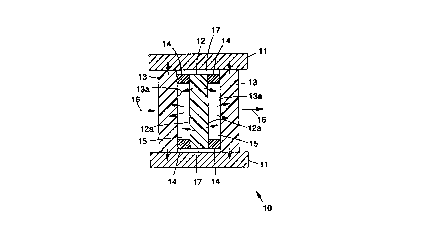
Fig. 2 shows a partial cutaway diagram of a laser crystal module that forms
part of a laser system that incorporates conductive face cooling in accordance with the
3 o principles of the present invention; and
Fig. 3 shows a second partial cutaway diagram of the laser crystal module of
Fig. 2.
t '.
20q3q60
3b
DETAILED DESCRIPTION
Referring to the drawing figures, Fig. 1 illustrates a portion of an optical
system 10 that incorporates conductive face cooling in accordance with the principles
of the present invention. Fig. 1 is not drawn to scale. More specifically, Fig. 1 shows
a portion of a laser system 10 that incorporates a laser crystal 12 that is secured in an
aluminium or other metal housing 1 1. It is to be understood that the laser crystal 12
may be any optical element that is employed in the laser system 10, and may include a
0 laser crystal or a nonlinear frequency conversion crystal, for example. The housing 11
may also be made of heat conducting materials other than metal.
4 2~493~fi~
The present invention provides a technique for cooling the laser crystal 12 or
nonlinear harmonic generation crystal, for example, such as a KTiOPO4 (KTP) crystal,
whereby the crystal 12 is cooled using heat conduction to adjacent heat conducting
media 13 through optical surfaces 12a that constitute its clear a~.lu,~,. Typical heat
5 conduching media 13 may comprise sapphire optical windows, for example. The heat
may be ~ Ç~ d (illustrated by the arrows) to the heat confll~on media 13 by direct
contact whereby the laser crystal 12 is placed in contact with adjacent surfaces 13a of
each of the heat conducting media 13. Alternatively, as was de~ol s~ i in an embod-
iment of the present invention that was reduced to practice, heat may be transr~10 through a narrow gas-filled gap 15 disposed between the optical surfa~es 12a and each
of the adjaoent heat conduchng media 13. The gas-filled gap is typically on the order of
0.00025 inches in ~hiC~n~os~ The gas employed in the gap 15 may be filled with air or
hydrogen, or other suitable gas, de~n-l;..g upon the laser opcl~ting wavelen~h The
gap 15 may be formed by placing an ~ring, dielechic spacer, or shim 14 ~l~.oen the
crystal 12 and the heat conduc~ing media 13. The ~iel~ic spacer may be formed bydepositing a thin film onto the surfaoe of the heat conduchng media 13. The crystal 12
does not directly contact the housing 11, as is shown in Flg. 1 by the gaps 17 between
the upper and lower edges of the crystal 12 and the adjacent portions of the housing 11.
The advantage of using the nalTow gas-filled gap 15 is that the s~r~ccs 12a,
13a do not contact, and thus there is no risk of ~l~mage to the optica~ surfaces 12a, 13a
during the assembly process, and anti-reflection co~hing~ on the optical sulr~ccs 12a,
13a function in a noqmal manner. The gap 15 may be foqmed by placing thin shims 14
or sp~ers between the laser crystal 12 and the heat-conducting media 13. The gap 15
may also be formed by vacuum depositing a dielectric film (0.00025 inches thick) at
selected locations on the heat-conducting media 13 or around the entire pC.~b~
thereof where the crystal 12 contacts the heat-con~ucting media 13. ~ition~lly, the
gaps 15 m_y be fo~med by vacuum d~posiling the dielectric film on one of the heat-
conclucting media 13 and appropliately m~rhinin~ the housing slightly larger than the
thickness of the crystal 12 (by 0.00025 inches). The crystal 12 is placed against the
film on one side and since the housing 11 is slightly la~rger than the crystal 12, when the
second heat-con(lucting me~ium 13 is pl~ed in contact with the housing 11, the second
gap 15 is formed. Consequently, in this last-described arrangement a second shim 14
is not needed.
An optical device in~ol~la~lg the heat removal principles of the present
invention has been reduced to prac~ he device ~at was built and tested comprisedtwo second harmonic genera~on (SHG) modllles 30, each using a KTiOPO4 (KTP)
crystal as a nonlinear medium Two different cross sectional diagrams of one of these
s 2~33~60
modules 30 are shown in Figs. 2 and 3. Fig. 2 shows a partial cutaway diagram of a
laser crystal module 30 that forms part of a laser system that incorporates the cooling
technique in accordance with the principles of the present invention, while Fig. 3
shows a second partial cutaway diaglarn of the laser crystal module 30 of Fig. 2.
S The KTP crystal 22 is disposed in an al~l.. nulll housing 11 and two small air
gaps 15 are located at the interface between the crystal 22 and sapphi.c plates 23
disposced on either side of the crystal 22. The sal~phi-c plates 23 are secured to the
housing 11 by means of two retainers 38 that are secured to the housing 11 by screws,
for example. Two ~rings 39 are d;~,ose~ between the retainers 38 and the sal)phi,c
windows 23. Resistive heaters 41 and heat spreaders 42 are secured by means of
springs 43 and cover plates 44 and screws, for example, to the housing that are
employed to heat the KTP crystal 23 to a predete.~led tc~xlatu e. A tel~ldlulc
sensor 46 is employed in a feedback cont~ol loop to control the te..~l4.O~ e of the KTP
crystal 23.
Intemally ge.l~lated heat from the crystal 22 is cond~A through the small air
gaps 15 to the sapphire plates 23. The sapphilc plates 23 then collduct the heat to the
aluminnm housing 11, and by means of heat pipes or other means (not shown), to an
external cold plate (not shown).
The effect of this cooling method was theoretically verified using finite ~lf ~
20 themnal analysis. In the case where a t~Ait;on~l method of ~nsverse heat condu~tion
is used, the thennal gradient ~T developed across the crystal 22 is e~ d by ~T =aPt47~K = 8~C, where ~ = 0.06/cm is the absolption coefficient, P = 50W is the power
in an applied l~r beam, arîd K = 0.03W/cmpC is the thermal conductivity of the KTP
crystal 22. This is far in excess of the approA;...~ely 2~ limit~tion on the thermal
25 gradient that is desired to ~ in~in efficient L~uency conversion. However, using the
approach of face-cooling in accordance with the principles of the present invention, the
f;nite element thermal model shows that this ~quirement is met.
This device including two SHG modules 30 was tested. No deg~adation in
performance was seen under 20Hz operation, whereas in prior tests not using this30 thermal m~n~gement approach there was a 10% degradation due to the onset of thermal
gradienLs within the module 30.
Thus there ha~s been described new and improved conductive face-cooled optical
elemenLs for use in high power laser systems. It is to be understood that the above-
described embo-lin~,nLc are merely illustrative of some of the many specific embodi-
35 ments which le~l~sent appli~ations of the principles of the present invention. Clearly,numerous and other arrange~ s can be readily devised by those skilled in the art
without departing from the scope of the invention.