Note: Descriptions are shown in the official language in which they were submitted.
~ 2--
~, 2~ a~2
A SYS~EM AND METHOD FOR TRAI~T5MTSSION OF
BURSTS OF DIGITAL INFORMATION
RA~ (.R~ND OF THE INVENTION
Field of Invention
The present invention relates to the digital
tr~n~ Tsion of information; and more particularly, to a system
and method for transmltting successive bursts of digital
information. Although the present invention is suitable for u~e
ln many different types of communication systems, it 18
particularly advantageous in cellular i r~tion systems for
transmitting frames of digital information; and i~ herein
described in connection therewith.
Discussion of Related Art
A ~elllllAr - irAtion system is a mobile t~rh~n~
service wherein radio cv~ r~ is divlded into cells . Bach cell
is assigned a number of available radio frequencies. The same
frequencies or ~h~nnelE uf;ed Ln one area or cell are ~180 used
for areas that are spatially separated from one anoth~r. A
mobile telephone station transmits and receives control and voice
communication information from a basQ station within the same
cell. The base stations are controlled by ~ cel llll~r system
switching and control network that provides connection with the
world wide tsl~ i cations network. A call in pco~ . ~88 il~ not
lnte. upted as the mobile st~tion travels from one cell location
to zmother, since the system provides for automatlc rea~si;
to an available channel within the other cell. Some of the
assigned ~hnnn~lR are used for control functions, such as
locating a mobile station, for example, and the c~ ~in;n~
~-h~nnel~5 for voice communication.
In order to provide superior non-interf ering
1-r~nRmi R8iOn and reception, a8 well as compatibility ~mong many
differ~nt mobile stations and base stations in different parts of
the world and the ~J-r)~h;lity of communicating with the world wide
--3--
. .
~ 2~9~0~2
telephone network, varlou~; operational and materlal
specif lcations and standards were developed to whLch all
suppliers and users are obliged to follow.
A mobile station that operates in the digital mode is
required to use an RF band which is divided into two separate 25
NHz wide segments, each consisting of 832 individual ~h~nnslY.
The f irst segment contains the mobile station transmit rh~nne
and the second segment, the moblle station receive rhAnn~ h~
effective maximum radiated power (ERP) for various
classifications of mobile stations is required to be from 0.6
watts to 4 watts d~pen~n51 on the classification.
Also, each channel for digltally transmitting
information is required to have a frame format; that is, ~ach
channel radiates a succession of frames, each of which has a
duration of forty milliseconds, ~nd constitutes one cycle of a
regularly recurring s~ries. Each frame has six slots and each
slot has 162 symbols and a duration of 6 . 67 milliseconds . Each
~ymbol is made up of 2 bits of data. Each slot contains a
separate burst of RF energy that is required to ramp up to peaX
power during a predet~rm~ n~d number of symbols at the ~e~i nn i n~
of each slot and ramp down to zero power during a predet~rmin-~d
number of symbols at the end of each slot.
It has been de~erm~ n~ that an RF power output of a
digital channel that increases or ramps up, or decreases ramps
down, from a peak value, at too great a rate at the be~nnin~ and
end of a slot causes spectral splattering of th~ transmitted
signal; and an RF power output that ramps up or down at too slow
a rate results in an overlapping of the slots and undesired
interf erence between two user ~ 8 slots .
It has been det~rm~ned by the cellular 8~An~iAr~sl
com~nittee that tr~npm~Rsion is to be effected by ramping up to a
peak voltage at the start of each burst during the first three
symbols of a slot; and a ramping down of the burst voltage at the
-
~ 209~0~2
- : -- 4 --
end of each burst beginning~during the last three
symbols of the slot.
Conveutionally, a transmitter that has a
digital channel and a frame format has six bursts per
. slot with Dnly one mobile staEion using the channel
at any one time. I~ such a system, a 6 tap spectral
filter can be used that typically has coefficients
sufficient to effect a peak power ramp up within the
first three symbols, and a power ramp down from peak
power within the last three symbols of a burst.
It has been proposed to allow multiple
users to share common channels in order to increase
the capacity of the system. For example, three
different users may use alternate sIots of each
15 ~ = frame. The sharing of each fra~ne tends to cause an
overlap of the data of the slots, which creates noise
and inferior communication.
In order to improve the spectral response
of a shared channel, a finite impulse response filter
having a greater number of tapg ig llti 1 i 75fl,
However, this advantage is offset by the slower ramp
up time to peak power and the slower ramp down time
from peak power for each burst. Thus, since optimum
ramp up or down is not feasible with the more
resolute f1lter, a separate ramp generator is
required to be connected to the output power
amplifier in order to conform to the desired standard
and provide optimum ramping of the power output.
S~IMMARY OF THE INVENTION
3 0 - ~One c f the advantages of an aspect of the
present invention is a system and method for
transmitting digital information wherein the optimum
ramping of the RF voltage of the individual bursts is
accomplished in a relatively simple and cost-
3 5 f ~ f ~ ; vf ~ r - n n f ~ r, ~
An advantage of an aspect of the present
invention is a transmitter and method for increasing
~ .A
209~0~2
- 5
the resolution of spectral f; 1 tPr;n~ of digital
information without deviating from the optimum
ramping of ~the RF out~out power of frames commonly
shared by a plurality of transmitters.
Additional obj ects and advantages of the
invention will be set forth in part in the
description which follows, and in part will be
obvious from the description, or may be learned by
practice Qf the invention. = ~he obj ects and
advantages of the invention will be realized and
attained by means of the elements and combinations
particularly pointed out in ~he appended claims.
To achieve the objects and in accordance
with the purpose Qf the inventio-n, as embodied and
broadly described herein, the invention in one
embodiment thereof is a system for transmittlng
successive bursts of digital information c~ntil;n;ng
multiple symbols, each burst ramping up from zero
power output to a peak power output and ramping down
f rom the peak power output to zero power output at a
respective beginning and endi~g of aach burst, ~aid
system comprising a digital data source for
generating data corresponding to at least o~e of
coded voice=and control information; symbol mapping
means coupled to ~he digital data source for
generating a series of sy=mbols having in-phase (I)
and quadrature phase - (Q) components corresponding to
the generated data, filtering means coupled~to the
symbol mapping means for spectrally filtering the
series of I and Q ~ymbol components, detecting means
coupled to the filtering means for detecting a start
of a ramp up and a ramp down of ~ each burst; zero
forcing means coupled to ~he filtering means and the
detecting means for forcing predetermined symbols to
a zero value to control ramping up and ramping down
of the power output; modulating means coupled to the
zero forcing means for modulating the filtered
'' .A
, _ .. ... , _ _ .. ... . .. . . .... . .. ........
2094D~2
~
-- 6
symbols of: each bur8t; and means including a power
amplifier for outputting modulated symbols.
In another aspect, the invention comprises,
a method for transmitting succes8ive~bursts of
digital information in a commu~ication system, at a
power output that is ramped up at the beginning of
each burst and ramped down at the end of each burst,
comprising the steps of: generating digital data
corresponding to at least one.of coded voice and
control information; generating in phase (I) and
quadrature phase (Q) c~mrr~nPntR corresponding to the
generated digital data; filtering spectrally the I
and Q symbols; and controlling preselected filtered
symbols of~ each burst for det~rm;n;n~ the ramping of
the transmitted output power.
Other aspects o~ this invention are as
follows:
A mobile cellular transmitter for
transmitting succeRsive frames of digital
info=rmation, each frame~c~-nti;;nln~ a burst of RF
energy, each burst cr nt;3;n;n~ multiple symbols and
ramping up f rom zero power output to a peak power
output and ramping down from the peak power output to
zero :power output at a respective beginning and
ellding of each burst, said transmitter comprising:
a digital data source for.~generating data
corre~ponding to at least one of coded voice and
control inf ormat ion;
symbol mapping means coupled to the digital
source data for generating a series of symbols having
in-phase (I~ and quadrature phase (Q) components
corresponding to the generated data;
a finite impulse response filter having at least
eight taps coupled to the symbol mapping means for
spectralIy filtering the I and Q symbol components;
detecting means coupled to the filter for
detecting a start o~ a ramp up and a ramp down of
each burst;
- A
2~9~2
~
- 6a -
a zera~ forcing circuit coupled to the filter and
the detecting means for forcing predetermined symbols
of each burst to zero value to control ramping~ up and
ramping down of the power output;
a quadrature modulator coupled to the zero
forcing circuit for modulating the sum of the output
symbols of each burst; and
means in~ l;ng a power amE~lifier for radiating
the modulated symbols. ~
. . .A method for transmitting successive bursts
of an RF power output, in a communication system,
comprising the steps of:
generating digital data cor~responding to at
least one of coded voice and control information;
~ :generating in phase and quadrature phase
components corresponding to the generated digital
dat a;
ramping up the RF power output at a start of
each burst to a peak power corYesponding to clock
time of a predetermined number of non-zero symbols;
and ramping down the R~ power output from peak power
coYresponding to the clock time of a predetermined
number non-zero value symbols at an end of .each
burst;
_ detecting the start symbol and end symbol of
each burst; and
forcing to zero power output at least the first
and last symbol of each burst to decrease the ramping
time of the power output.
: ~ A system for mo~ t;n~ the transmission
power level of successive bursts of digital
information cnnti~;n;n~ multiple symbols, each burst
ramping up from zero power output to a peak power
output and ramping down from the peak power output to
zero power output at a respective beginning and
ending of each burst during a predetermined number of
symbol time periods, the system comprising:
,_
'
~ 209~
- ~b -
a waveform map for generating a series of
symbols having in-phase~ (I) and quadrature phase (Q)
components corresponding to some data;
a filter coupled to the waveform map for
spectrally filtering the I and Q symbol components,
the f ilter being operative to ramp up from zero power
to peak power and ramp down from peak power to 2ero
power at a respective beginning and end of each burst
during a number of symbol time periods greater than
' sai'd predetermined number of symbol time periods;
a detector coupled to the ~ilter for ~ t;n~ a
start of a ramp up and a ramp down of each burst;
a zero forcing circuit coupled to the filter and
the detector for torcing predete:rmined filtered
sy[nbols to zero value to cause the ramping up and the
ramping down of the power output to occur during the
predetermined number of symbol time periods.
A method for moaulating the transmission
power Levelsof ~ucces~i~e bursts each burst
comprising,a sequence of symbols, the method
compris ing:
generating in-phase and ~lAfl~A~ll~e phase
compo}lents corresponding to data;
ramping up the pQwer output at the start symbol
o3~ each burst to a peak power corresponding to the
clock time of a predetermined number of non-zero
symbols;
ramping down the power output f rom peak power
corresponding to the clock time of a predetermined
number Qf non-zero value syTbols at the end symbol of
each burst;
detecting the start symbol and end symbol of
each burst; and
forcing to zero power output at least the first
35 , ana Iast sy~bol of each burst to decrease the ramping
time of the power QUtpUt.
It is to be understood that both the
.Ar ~oregoing general description and the following
- _ _ _ _ _ _ _ _ __ _ _ _ _ _ _ _ _ __ _ _ _ _
~ 2U940a2
-- ~c
~ ti~;lo~l des-cription are exemplary and explanatory
only and are not restrictive of ~he invention, a~
claimed .
The accompanying drawings, which are
incorporated in and constitu~e a part of ~ this
specification, illustrate one e~odiment of the
invel:ltion and together with the description, serve to
explain the principles of the invention.
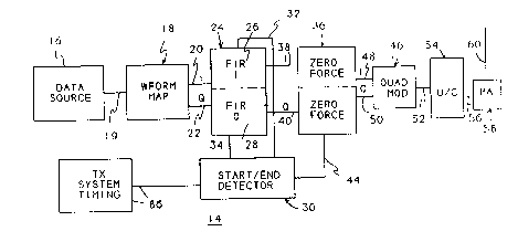
Rl~Tl;!l~ n~-~RIpTIoN OF T~5 DRAWINGS:
. ~_Eig.~ 1 depicts schematically a frame of a
digital . In; ~ ~tion channel generated by a system
incorporating the present invention;
Pig. 2 depicts schematically one of the
slots of the frame of Fig. 1;
Fi~. 3 is a schematic block diagram of a
digital portion of a transmitter incorporating the
present invention;
Fig. 4 i8 a graphical representation of the
phases of a waveform map for forming I and Q
comFonents;
Fig. 5 is a schematic diagram of a finite
impulse response (FIR) filter of the system and
method of the present invention;
Fig. 6 is a graphical representation of a
filter waveform ana the corresponding coefficients of
the f ilter of Fig . 5;
Fig. 7 is a block diagram of the zero force
circuit of the system of Fig. 3 in accordance with
the present invention;
3 0 ~ ~ Fig . 8 is a schematic block diagram of the
~tartlend detector of the system of the present
inventiorl;
,"~
,A
;. . ,
~7~ 209~52
_
Fig. g 18 a graphic~l lllustration of the oper~tLng
states of the f ilter taps of Fig . 6 during detection of the start
and end of a slot;
Flg. 10 is a timing diagram depicting the operation of
the start/end detection of the system of the present invention;
and
Fig. 11 is a graph illustrating a comparison of the
ramp voltage at the beginning ~nd end of a burst both with and
without the present invention.
pESCRIPTION OF T~E PREFERRED BMBODINBNT
Prior to discussing the system and method of the
present invention; a description of the frame and slot protocol
utilized in connection with a cellular system will be briefly
described in connection with Figs. 1 and 2 in order to better
understand the invention . Fig . 1 illustrates a f rame of
information generally referred to at 10, which is transmitted
every forty m; ~ econ~ or at a rate of 25 frames per second.
Frame 10 has six slots, referred to as slots 12. Of the slots
12, two slots A may be used by one mobile station, two slots B
another, and two slots C by a third station or s~hncr;h.or for
carrying on conversatlons simultaneously. Each slot ~g_nts
an individual burst of RF energy of a duration of 6 . 67
~illiseconds. Referring to Fig. 2, one of the slots 12 has
several fields, ~ guard time field G, a ramp time field R, a
synchronization field SYNC, a sixteen bit data channel, two data
rh~nnelF~ of one hundred twenty-eight bits each, and a coded
digital verification color coded slot CDVCC. The slot ramps up
from zero output to peak output voltage at the be~nn;nq of each
slot as shown at R and ramps down from the peak voltage at the
end of each slot (not shown). The guard time portion is between
individual bursts of each slot.
Reference will now be made in detail to the present
prQferred ~ t of the invention, an example of which is
illus~rated in the a~ -nying drawings. Wherever possible, the
--8--
~ 209~1~52
s~me reference numbers will be u~ed throughout the drAwinga to
refer to the same or llke part~.
The system of the present invention comprises a
transmitter that has a data source, a waveform map, a finite
impulse response filter, a zero force circuit, a start/end burst
detection circuit, a quadratur~ modulator, an uycc,.,~ er, a
power ampliiier and an antenna.
RQferring to Fig. 3, and as ~ e~i hQrein, a
tranamitter generally referred to as 14 is configured to produce
successive bursts of digital information, each of which ramps up
and ramps down RF output power at the ~e~nn;ng ~nd ~nd of each
burst during the oc~rrRnce of a yl~Q~ d number of symbols.
Transmitter 14 comprises n data source 16 for generating digital
data cor~esyoAding to coded control and/or voic~ lnf~- tion. A
waveform mapping device 18 has an input l9 from the data source
and converts digital data to in-phase (I) and qu~d.~,lu.~ phasQ
(Q) c~ .~ ts at outputs 20 and 22, which are input to a filtQr
24, which is a preferably a finite impulse ~syun~ (FIR) fllter,
having I and Q sections 26 and 28 for filtering out the sidel~be~
of the I and Q e ts . As herein: '1 ed, filter sections
26 and 28 each have preferably eight st~ges or taps. Start/end
burst detecting circuit 30 is connected to outputs 32 and 34 of
filter sections 26 and 28 for detecting th~ start of a ramp up or
ramp down of ~ach burst.
In accordance with the invention, zero f orcing means i~
coupled to filtering means for forcing pred~t~rm~ned Isymbols to
zero value to control ramping up and ramping down of the power
output. As herein ~ d, zero forcing circuit 36 has inputs
38 and 40 connected to filter sections 26 and 28, and input 44
connected to output 44 of start/end detection circuit 30 for
controlling the symbol values applied to a quadrature modulator
46 over lines 48 and 50. The modulator 46 has an output 52
connected to uyco--~ er 54 for increasing the LLe~5lU~nl_Y of the
--9--
-' 2~9~052
output, which in turn i8 connocted to input 56 of power amplifier
58. An antenna 60 radLates the bursts of power from the power
ampli f ier .
For the cellular appllcation of the present invention,
data sourc~ 16 provides digltal data in the form of 2-bit symbols
which are modulated into a differential quadrnture phas~ shift
key (DQPSR) waveform. ~he data can contain coded voice and/or
control information repre6ented by 00, Ol, 10, or 11, input to
waveform map 18 for conversion into in-phase (I) and guadrature
phase (Q) ~o~lo.~ts that COLL~ O~Id to 8 p~ssihle phas~ number~
or values in accordance with the following table of values.
5~ Phase ~1
1.0 0
. 707 . 707 2
0 1.0 3
_ . 707 . 7 07 4
-1.0 0 5
_.707 _.707 6
0 -1.0 7
. 707 - . 707 8
P~eferring to Fig. 4, a graph 60 depicts the eight
possible coorl~n~te locations which ~;oLL~ d to the I and Q
values of the above table. When both I and Q values are at zero
amplitude, the location is at the ~unction 62 of the coo~in~t~s.
Pilter 24 is illustrated in Fig. 3 as having two
sections. These sections may be separate modules. A s1ngle
module or filter may be u6ed in place of the pair by using a time
sharing arrangement in a well known manner. For purposes of
clarification, the filter will be d~ r~hed as two sections or
modules. Section 26 of filtQr 24 accepts the (I) phase and
filter section 28 accepts the (Q) phase values from waveform map
18, and filters the data to perform spectral smoothing of the
signal, as previously mentioned. Although it is preferred that
filter 24 has length of 8 in order to assist in the reduction of
-
10--
~ 2Qa~os2
out of b~md power croated in tho digit~l modulation process, such
a filter creates a peak output after recelving four non-zero
symbols. Thus, the ramp up time of the filter i8 four symbols.
The ramp down time is symmetric which is also four symbol clock
times. Referring to Pig. 5, filter sections 26, 28 each have
eight stages or taps referred to as X0 through X7. It should be
mentioned that even if it were a single filter, each of the
~. ts I and Q would be sub~ected to eight f ilter stages .
The I or Q values, as the case may be, enter the filter at X0 and
move successively each symbol clock time through X7, similar to a
shift register. At each stage or tap, the values therein are
multlplied by corresponding filter co~ff;~Qnts C0 through C7 at
respQctive multipliers 64 through 71. The products of each of
the multipliers are summed at adder 74 and output on lines 38, 40
to zero force circuit 36. Thus, a filtered output value occur~
at a time ~0~ 3pm.~;ng to each symbol clock time, and a shift or
cycle of the filter.
Referring to Fig. 6 the amplitude of each of the
coef f i cif~nts C0 through C7 is illustrated at 80 where e~ch
enlarged dot . ~p esents the amplitude of a coLle~on~ing filter
coefficient. As seen from Fig. 6, the connection of circles 80
define a filter waveform 82; and it isn~t until the fourth non-
zero symbol of the filter that the peak amplitude of the
multiplier coef f icient is reached .
Referring to Pig. 8, start/end burst detection circuit
30 includes an input 86 that recQives a start strobe signal from
a transmitter system timing module to begin transmitting. This
cauaes the first symbol of the slot to enter the filter and
provide an input to a delay circuit 88. Between bursts, the
circuit 88 is outputting a logic ~false~ signal over line 90 to
A~D gate 92. Bur~t detection 30 also ;nl~]lldes comparators 94 and
96 which determine whether or not an I or Q symbol on line~ 32
and 34 is zero. Both of these inputs are also zero between
bursts, which causes a logical ~true" to bQ output on line 99
--ll--
21~9~2
which is inverteq by inverter 100, thu~ applying a logical
~ false~- to line 102 and AND gate 92, whlch results in a ~low~
signal on line 44. After a delay of one sy~bol, line 90 goes
logic rtrue~, and the zero signal control is released. When one
or the other of the I and Q symbols is non-zero, an output
"false~ occurs on line 99, which 18 inverted at 100 to apply a
logic "true~ to AND gate 92 which together with the "false" on
line 90 keeps line 44 "low" for thQ fir~t nvA-s~e~u symbol of a
burst. When AND gate g8 does not conduct, inverter 100 applies a
"true" input on line 102 to AND gatQ 92. Thus, AND gate 92 is
"low" prior to the one ~ymbol delay by circuit 88 forcing the
first symbol applied to the modulator 46 to be zero.
A "true~ logic signal on both line 90 and 102 cause~ a
logic level "high~ on line 44 permitting the output of filter 24
to enter quadrature modulator 46. Thus, during the burst, the
logic level remains "high" on 44. A detection of a zero value on
both I and Q lines 32 and 34 causes AND gate 98 to conduct which
applies on input to delay circuit 104; and after a delay of six
symbols line 102 goes ~false~, which causes the output of AND
gate to conduct a 1~ low~ signal on line 44 .
Referring to Fig. 7, zero force module 36 includes
multiplexer switches 103 and 105 having an input from output 38,
40 of the respective f ilter sections 26 and 28 . Nul~ x~r
switches 103 and 105 have an input 44 that applies either a
"high" logic lQvel or a ~low~ loglc level signal from start/end
detector 30. While the signal on 44 is "high~, the mult~rl~Y~r
switch conducts the I and Q values on lines 48 and 50 to
quadrature modulator 28. When the signal on line 44 goes "low~,
the output of the multiplexer switcheY to the modulator 46 is
zero amplitude as indicated by inputs 107 and 109. The logic
levels on input 44 are controlled by the start/end detection
module 36 as previously described.
--12 -
= =2~9~2
A more det~ilod d~scription of the method and system of
the present Lnvention will be givQn in connection with Figs. 9,
10, and 11 in describing the overall operation of the system.
Between each burst, the filter taps X0 through X7 are
all set to zero as shown rt tap llne 108 of Fig. 9, thus,
providing n zero amplitude R~ power output. Upon entry of the
first non-zero value to tap X0, the zero values in the filter all
shift to the left as viewed by taps 110 of whlch now provides a
signal having a value of the product of C0 . a, ~t the output of
the filter. However, since the start/end detection module
recognizes thls non-zero value as the ~e~nnln7 of a burst, input
44 goes low, which in turn causQs multiplexer switches 103 and
105 to output a zero value to modulator 28, thus, providing no RF
input to u~cv~v~L~er 54 and power ~ l~fi~r 58. Upon entr~ of a
second non-zero output a2, valuQ a, shifts to the left as shown
at 66 which providQs a filter output value of a . C h a2 . C0,
the signal on line 44 goQs high which permits multiplexQr
switches 103 and 105 to output the filter valuQs to thQ
upc~ollvtsL~er 54 ~md power amplifier 58. Upon entry of the non-
zero value a4 (not shown) the power output peaks; and the burst
continues until the Qnd. The addition of values which decreases
the number of zero values in the taps and finally Qli3ninates all
the zero values in the filter does not cause an appreciable
difference in the peak v~lue of thQ power output. Toward the end
of the burst, the first four taps Xl, X2, X3 and X4 su~c~ively
fill with zero values as ~hown at tap line 114, which defines the
end of the burst with an output that coLL~e~,vnds to the sum of C4
X + C5Y + C6Z + C7W. This is the last "peak" and first ramp of
the signal. Upon entry of the fifth zero value, as shown by the
line of taps 116, the signal ramping down as required by
cormnunication standards with the output of the f ilter decreasing
to the sum of C6X + C7Y +C8Z. ~pon entry of the sixth zero value
to the filter as shown by tap line 118, the output d~cre~e~ to
the sum of X.C6 + Y.C7, which Ls the final ramp down output
--13--
20~52
sign~l permitted by the offlcial st~ndards. Upon entry of the
seventh zero value as shown by tap line 120, the start/end
detection module 36 cause~ input line 44 to go low which causes
multiplexer switches 103 and 105 to output a zero value, thus
preventing X . C7 from being applied to quadrature modulator 46.
Referring to Fig. 10, timing line 122 of each slot or
burst depicts a start signal at 124 and an end sign~l at 126 at
the end of each burst. At the beglnnlng of each burst, the zero
signal tlme line 128 Lndicates at 130 that it p~rmits the quad
modulator 46 to recelve a2 as the first ramp up clock symbol tim~
after forcing the output COLLe~ A~n~ to al to zero; 4nd the
zero force output of the zero force module goes "high" at 132 of
time line 134. Upon detection of the first zero magnitude symbol
as ~n~icate<l 4t 136 of time line 138, and after a delay of six
symbol clocks, the zero force signal is output as shown at 140 of
time line 142 forcing the output COL~4F~.~nti; n~ to al56 to zero
~f ter reaching tap X7 .
In su~mary, and referring to Fig. 11, after the start
of a burst, non-zero I and Q data enters the FIR filter, and thQ
filter begins to produce power out. As indicat~3d by Fig. 4, for
a length N filter, the first symbol will peak midway between the
first and last tap or in other words N/2. Similarly at the end
of a burst the FIR filter is filled with z~ros after the last
data is transmitted. For an N length filt~r the signal will go
to zero N/2 symbol times after the last symbol peaked at the FIR
output .
For certain applications the optimum operator and cell
standard requires the ramp-up/down times to be 3 symbols in
length. Thus, it would requlre an FIR of length six to meet
these ramp times. The standard also calls out for other
sp-?c~fication~ such as spectral limitations and modulation
accuracy to be met during the transmission of the burst, which
--14--
2~9~d!~2
require f ilter length2~ of at least eight . The ramp times of
these longer filters would not meet the standards without
limiting the ramp time to three clocks symbols.
Referring to Flg. 11, the output power profile of a
typlcal transmltter wlth a length eight FIR filter performlng
waveshaplng on the input I and Q values wlthout the beneflt of
the present lnvention is referenced to as 141. This profile
would not satisfy the standard for ramp times. The figure also
shows the output power profile 144 of the same transmitter, but
with the addition of the present invention. This profile does
satisfy the stAnAArA~ for ramp times, and also meets the spectral
L~v~se limitations and modulation accuracy.
At the end of the burst, the control circuit detects
the end of transmit burst when it sees a zero magnitude I/Q value
enter the first FIR tap value. The FIR filter continues to run,
but after its sixth output cycle, the output of the FIR is forced
to zero. This number is sixr because after the zero value is
detected, it wlll take three symbols for the last non-zero value
to "peak~', then three additional symbols of ramp-down are
allowed .
Having described the presently preferred system
t ~nd method of the inventlon, additional advantage~ and
modifications will readily occur to those skllled in the art.
For example, the system and method could be used in a central
station, a filter having more than eight taps may be used, and
more than one symbol may be forced to zero to obtain the optimum
ramping, for example. ~t~cor~in~ly~ the invention in its broader
aspects is not limited to specific details, e~ e5aAtatiVe
apparatus and illustrative ex_mples shown and described.
Departure may be made from such details without departing from
the spirit or scope of the general inventive concept as def ined
by the Arp~ntl~d claims and their equivalents.