Note: Descriptions are shown in the official language in which they were submitted.
WO 92/09143 PCT/US91/08362
-1- 2~~~1~~
MEMORY MAPPED KEYBOARD CONTROLLER
~ackcrround of the Invention
Field of the Invention
The present invention relates to facilitating control
within Industry Standard Architecture (ISA) compatible laptop
computers. Specifically, the invention involves a way to
alter conventional keyboard scanning methods to more
efficiently read a keyboard which is an integral part of the
computer.
Description of the Related Art
Conventional ISA (i.e. IBM-AT) compatible computers
utilize an integrated circuit (IC) intelligent peripheral
microcontroller to perform various control functions between
a master processor (the host--the master central processing
unit and supporting resources) and various peripheral devices.
Typical I/O functions performed by the peripheral
microcontroller involve scanning a keyboard and providing an
interface between peripheral devices and the host. The
microcontroller interfaces these peripheral devices with the
standard ISA data and control busses. The microcontroller
provides registers which enable it to function as one
peripheral device to the master processor. The
microcontroller performs the basic I/O functions for other
peripheral devices so the host does not have to use processor
time to perform these functions. The host only communicates
with the peripheral microcontroller which performs the
processing necessary to support the other peripheral devices.
The INTEL 8042 and 8742 integrated circuits are common
peripheral microcontrollers for the ISA compatible computer
architecture. The use of the 8042 and the 8742 integrated
circuits in laptop computers is undesirable because these
integrated circuits utilize older technology which consumes
too much power. For instance, the INTEL 8742 is a 50mA IC.
Moreover, these IC's operate in a continuous active mode in
which they continuously poll an input register flag to
determine if the host has written data to the input register
WO 92/09143 PCT/US91/08362
2094140
-2-
of the peripheral controller, a keyboard, mouse clock and data
signals to determine if the mouse has moved, and other I/O
peripheral devices to determine if data needs to be
transferred.
In laptop computers which can operate on rechargeable
batteries, any reduction in power consumption results in an
increase in battery life (i.e. time between battery
recharging). However, most presently available laptops
continue to utilize the conventional peripheral
l0 microcontrollers.
It is therefore desirable to provide a controller for use
in laptop computers which consumes substantially less power
than the conventional peripheral microcontrollers.
Newer technologies, such as CMOS (complementary metal
oxide semiconductor) exist which allow design of application
specific integrated circuits (ASIC) which consume less power
than the conventional peripheral microcontroller. Simply
implementing the conventional controller with CMOS technology
would decrease power consumption. However, the inefficient
active polling of conventional peripheral controllers would
continue to consume more power than is desirable because CMOS
circuits consume more power when active than when idle.
Moreover, under the conventional design, the keyboard
requires an additional IC to scan the keyboard matrix to
determine if a key has been pressed. The keyboard scanner
then determines which key has been pressed and converts the
key position into a scan code for transmission to the
conventional peripheral microcontroller. The peripheral
controller then forwards the scan code to the host. The extra
keyboard scanner IC consumes further power which is
undesirable.
Therefore, it is further desirable to eliminate the
separate IC which scans the keyboard and generates scan codes
for the peripheral microcontroller. Advantageously, the
peripheral controller provides all the keyboard control and
only scans the keyboard when a key has been pressed. This
reduces the power consumption of the computer, and thereby,
CA 02094149 1998-09-02
extends battery life.
Summary of the Invention
The present invention provides a relatively low
power peripheral controller which utilizes memory mapped
address decode architecture to expand I/0 control ports
and enhance interrupt service capabilities to allow a
single chip to control many laptop computer applications.
Extensive power management capabilities have been added
to the microcontroller to conserve power and to extend
l0 the battery life of a laptop computer.
The controller emulates the functions of the
previous peripheral microcontrollers so that software
written for a conventional ISA computer will operate on
computers incorporating the present invention. The
controller also contains a new keyboard scanner
controller that operates on an interrupt basis to
conserve power rather than continuously scanning the
keyboard. The present keyboard scanner also provides a
system for mapping a keyboard switch matrix into memory
or I/O space of the host such that multiple keys can be
read in a single machine cycle.
Other aspects of the invention include:
A memory mapped keyboard scanner for a peripheral
controller for use in a host computer system, said
peripheral controller having a core microprocessor having
addressable memory space and an input/output port, said
peripheral controller having a data bus and an address
bus coupled to said core microprocessor said keyboard
scanner comprising:
a keyboard switch matrix with a plurality of columns
and a plurality of rows;
a keyboard row data bus connected to said plurality
of rows, said keyboard row data bus comprising a
plurality of signals that reflect the logic states of the
rows; and
-3-
CA 02094149 1998-09-02
keyboard control logic configured to operate in
first and second modes, said keyboard control logic
comprising:
a detector coupled to said keyboard row data bus and
responsive to said signals on said keyboard row data bus
in parallel to provide an any-row indicator on an output
of said detector, a signal on said any-row indicator
signifying whether at least one of the rows of the
keyboard is active;
l0 a decoder coupled to said address bus and said
keyboard columns, said decoder responsive to a plurality
of pre-selected addresses on said address bus, said
addresses pre-assigned to the keyboard columns, said pre-
selected addresses within the addressable memory space of
said core microprocessor; and
a selector, said selector coupled to said address
bus, said keyboard row data bus and said input/output
port, said selector responsive to pre-selected addresses
on said address bus, said addresses assigned to said
keyboard row data bus;
wherein in said first mode, said decoder responds to
a first one of said plurality of pre-selected addresses
assigned to said keyboard columns to selectively activate
all of said columns in parallel, and said detector
monitors all of said rows to detect when at least one of
said rows becomes active because a key has been pressed,
and wherein after detecting at least one active row, said
keyboard control logic operates in said second mode
-4-
CA 02094149 1998-09-02
wherein said decoder responds to access operations
by said core microprocessor to others of said plurality
of pre-selected addresses assigned to the keyboard
columns to selectively activate individual columns in the
switch matrix one at a time, and wherein in said second
mode said selector responds to the pre-selected addresses
assigned to the keyboard row data bus to couple said
keyboard row data bus in parallel to said input/output
port.
A peripheral controller for use with a host PC
compatible computer system, said peripheral controller
having a core microprocessor coupled to a data/address
bus, said peripheral controller providing an interface
IS between said host and a keyboard having a plurality of
rows and a plurality of columns in a switch matrix, said
peripheral controller comprising:
a keyboard row data bus having a plurality of row
signal lines connected to said rows of said switch
matrix, signals on said data bus that reflect the logic
states of the rows connected to said bus, said keyboard
row data bus also selectively connected to the
data/address bus, wherein said keyboard row data bus is
configured to be read by said core microprocessor when
said core microprocessor executes a read operation from a
pre-selected address location assigned to said keyboard;
an address bus coupled through an address latch to
the data/address bus of said core microprocessor; and
a keyboard controller coupled to said columns, to
said keyboard row data bus and to said address bus, said
keyboard controller configured to operate in first and
-4a-
CA 02094149 1998-09-02
second modes, wherein said keyboard controller is
responsive to predefined address signals provided by said
core microprocessor on said address bus to activate all
of the columns in said switch matrix in parallel, in said
first mode, and further responsive to the signals on said
row signal lines in parallel to detect when at least one
of said rows becomes active, indicating that a switch has
been activated, and after detecting at least one active
row during said first mode, said keyboard controller
responding to predefined addresses provided by said core
microprocessor on the address bus to activate said
columns one at a time in the second mode and to select
the keyboard row data bus for connection to the
data/address bus of the core microprocessor to enable the
core microprocessor to detect which row and column
contain the active switch in said switch matrix.
A method of monitoring and scanning a keyboard
switch matrix mapped into memory or I/O locations such
that multiple keys are read in a single machine cycle,
said switch matrix comprising a plurality of switches and
having rows and columns, and said method implemented with
a core microprocessor having addressable memory space,
said method comprising the steps of:
assigning selected addresses within said addressable
memory space of said microprocessor to each of said
columns of said switch matrix;
providing a column activation decoder connected to
said switch matrix and responsive to said selected
addresses, said decoder activating all of said columns in
response to a first one of said addresses and activating
-4b-
CA 02094149 1998-09-02
selected columns one at a time in response to other of
said addresses;
providing a keyboard row bus having a plurality of
signal lines connected to said rows of said switch
matrix;
applying said first one of said addresses to said
decoder to activate all of said columns;
monitoring said keyboard row bus and waiting for one
of the plurality of signal lines to become active;
when one of said signal lines becomes active,
applying said other addresses one at a time to said
decoder to individually activate said columns;
reading the keyboard row bus in a single machine
cycle for each of said other addresses to determine if a
selected row is active within the activated column; and
when a selected row is active, combining the row
location with the activated column to detect the active
switch.
A keyboard controller for use with a computer
keyboard matrix having columns and rows, said keyboard
controller comprising:
a core microprocessor in communication with a host
computer, said core microprocessor having at least one
input/output port and at least one interrupt port, said
core microprocessor having an active mode and a low power
mode;
a plurality of keyboard instructions stored in
memory and executable by said core microprocessor, said
plurality of keyboard instructions comprising
instructions for driving the keyboard matrix and for
-4c-
CA 02094149 1998-09-02
reading the keyboard matrix, wherein said core
microprocessor does not execute said plurality of
keyboard instructions in said low power mode and wherein
less electrical power is consumed within said core
microprocessor when said core microprocessor is in said
low power mode than when said core microprocessor is in
said active mode;
a plurality of keyboard column driver lines coupled
to keyboard columns to selectively cause said keyboard
columns to be driven at the same time;
a plurality of keyboard row sense signal lines
coupled to the core microprocessor input/output port; and
keyboard control logic having an output coupled to
said at least one interrupt port of said core
microprocessor, said keyboard control logic configured to
generate an interrupt on said output if any key in said
keyboard matrix is pressed, wherein if said core
microprocessor is operating in said low power mode, said
interrupt activates said core microprocessor to resume
active mode operation and execute said keyboard
instructions.
A keyboard controller for use in a host computer
having a keyboard switch matrix with columns and rows,
said keyboard controller comprising:
a core microcontroller in communication with said
host computer, said core microcontroller having at least
one input/output port and at least one interrupt port,
said core microcontroller having an active mode and a low
power mode, wherein less electrical power is consumed
within said core microcontroller when said
-4d-
CA 02094149 1998-09-02
microcontroller is in said low power mode than when said
core microcontroller is in said active mode;
a plurality of keyboard column driver lines coupled
to keyboard columns to selectively cause said keyboard
columns to be driven at the same time;
a plurality of keyboard row sense signal lines
coupled in parallel for simultaneous reading by said
input/output port; and
keyboard scan logic having an output coupled to said
at least one interrupt port of said core microcontroller,
said scan logic configured to drive all of the columns
active and configured to detect if any key is pressed
while the columns are active, the scan logic generating
an interrupt on said output to activate said core
microcontroller to operate in said active mode, to scan
said keyboard matrix, and to communicate a scan code
representing the active switch in the matrix to the host
computer.
Brief Description of the Drawings
Figure 1 is a block diagram of the peripheral
controller system according to the present invention.
Figure 2 is a block diagram of the host interface of
the system.
Figure 3 is a diagram of the host and core
(input/output) I/O buffers.
Figure 4 illustrates the host I/O control block.
Figure 5 illustrates the data bus register buffers
for the host.
Figure 6 illustrates the address/data latch for the
microcontroller core central processing unit (sore CPU)
Figure 7 illustrates the data bus status register.
-4e-
CA 02094149 1998-09-02
Figure 8 illustrates the address decoder/bus
multiplexes circuit for the microcontroller core.
Figure 9 illustrates a diagram of the keyboard
scanner of the present invention.
Figure 10 illustrates an exemplary portion of the
keyboard switch matrix of the present invention.
Figure 11 illustrates a schematic diagram of the
interrupt controller of the present invention.
Figure 12 illustrates a schematic diagram of the
boot-loader circuit of the present invention.
Figure 13 illustrates a schematic diagram of the RAM
controller of the present invention.
-4f
WO 92/09143 PCT/US91/08362
-5- 2~9!~~.~9
Figure 14 illustrates a flow chart of an exemplary boot-
load program sequence executed during boot-load of the
microcontroller core.
Figure 15 illustrates a gate A20 bypass controller of the
present invention.
Detailed Description of the Preferred Embodiment
The present invention will be described in the context of
component oriented logic with an independent microprocessor.
In a preferred embodiment, the entire system is implemented in
an application specific integrated circuit (ASIC) which
includes the microprocessor within the ASIC.
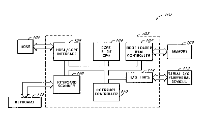
The block diagram of Figure 1 illustrates the principal
system units of the present invention. The computer system
100 comprises a master processor and supporting platform
resources (the host) 102 such as an INTEL 80x86 motherboard,
a peripheral controller 103, a memory 109, a keyboard 112, and
serial input/output (I/0) peripheral devices 113. The
peripheral controller 103 includes a microcontroller core
central processing unit (CPU) 104, a host/core interface 106,
a boot loader and RAM controller circuit 107, a keyboard
scanner 108, an interrupt controller 110, and I/O lines 114
connected to the serial I/O devices 113.
The peripheral controller 103 emulates a conventional
peripheral microcontroller such as an INTEL 8042 or 8742 and
performs additional functions discussed herein. The
peripheral microcontroller 103 described can be implemented in
a low power CMOS application specific integrated circuit
(ASIC).
The Microcontroller Core
The microcontroller core CPU 104 comprises, or emulates.
the functions of, an INTEL 80C31 family microcontroller as is
well understood in the art. The core CPU 104 is programmed to
manage the operations of the peripheral controller 103.
The Host/Core Interface
The host/core interface 106 comprises a number of
different functional blocks. These blocks are shown in Figure
2, and include a set of tri-state input/output (I/O) buffers
WO 92/09143 PCT/US91/08362
2094149 -6-
120, host I/0 control 122, data bus I/O register buffers 123,
a status register 124, an address decoder/bus multiplexer
circuit 126, address/data bus latches 130, and a gate A20
bypass controller 650.
The I/O Buffers
The tri-state I/O buffers 120, depicted in Figure 3,
include a host I/O buffer 140 and a microcontroller core I/O
buffer 160. These buffers 140 and 160 are similar.
The host I/O buffer 140 provides a buffer which utilizes
an XD_P[0..7] bi-directional host data bus 150 connected to a
conventional host I/O bus such as an Industry Standard
Architecture (ISA) bus as is well understood in the art. An
XDO[0..7] output signal bus 152 carries a set of signals from
the peripheral controller 103 for output onto the XD_P[0..7]
host data bus 150, and an XDIN[0..7] input signal bus 154
carries signals to the peripheral controller 103 from the
XD-P[0..7] host data bus 150. The core I/0 buffer 160 also
uses an XD OE enable signal line 156 to gate signals on the
XDO[0..7] signal bus 152 to the XD_P[0..7] host data bus 150.
Any data from the host on the XD_P[0..7] host data bus
150 will propagate through the buffer onto the XDIN[0..7]
signal bus 154 for use within the peripheral controller 103.
The core I/O buffer 160 provides a tri-state buffer for
the core CPU 104. The core I/O buffer 160 utilizes an
AD_P[0..7] bi-directional address/data bus 172 connected to
the core CPU 104 Port 0 (corresponding to Port 0 of an Intel
80C31) as is well understood in the art. An AD[0..7] output
signal bus 174 carries signals from the peripheral controller
103 for output to the core CPU 104, and an ADIN[0..7] input
signal bus 176 carries signals from the core CPU 104 for input
to the peripheral controller 103. An active AD_OE signal line
178 allows the signals on the AD[0..7] signal bus 174,
propagate..through the buffer to the AD_P[0..7] address/data
bus 172.
When the core CPU 104 places data on its Port 0 data
lines, the signals propagate through the core I/O buffer 160
to the ADIN[ 0. . 7 ] signal bus 176 for use by the peripheral
WO 92/09143 PCT/US91/08362
7
controller 103.
The Host IJO Control Circuit
The peripheral controller 103 requires a number of
control signals. Many of these signals are provided by the
host I/O control 122, depicted in Figure 4. The host I/O
control is relatively straight forward and will be explained
in functional form.
The host I/O control 122 utilizes signals on an XIOW_
(I/O write) signal line 264, an XCS_ (chip select) signal line
224, a CLKIN (CLOCK) signal line 226, an XIOR_ (I/O read)
signal line 228, an XA2 (address line 2) signal line 200, and
a RESET_ signal line 216. These signals are the standard I/O
write, I/O read, chip select for the conventional 8042 or 8742
peripheral controllers, clock, and reset control signals from
the host 102 as are well understood in the art.
The interface control 122 also uses a MI8F (mask input
buffer full flag) signal line 270, and a BOOT (core is
executing boot load) signal line 271.
The interface control 122 provides an SIBF (set input
buffer full) signal line 210, an HWRP- (host write pulse)
signal line 260, an HWR- (host write) signal line 202, a WR60_
(host write to port 60) signal line 229, a WR64_ (host write
to port 64) signal line 230, an IA2 signal line 232, an HRD_
(host read) signal line 234, a RD60_ (host read from port 60)
signal line 236, a RD64_ (host read from port 64) signal line
235, and the XD OE signal line 156.
The HWRP_ signal line 260 is driven active by any write
to port 60 or to port 64 by the host 102 (the XIOW_ signal
line 264 and the XCS_ signal line 224 are active). The HWR_
signal line 202 is driven active under the same conditions as
the HWRP_ signal line 260, but three clock cycles after the
HWRP_ signal line 260 goes active. The SIBF_ signal line 210
is driven active upon a write to port 60 or to port 64 by the
host 102 (the XIOW- signal line 264 and the XCS- signal line
224 are active) when the MIBF signal line 270 is not active
(the input buffer full flag is not masked), and the BOOT
signal line 271 is not active (the controller 103 is not
WO 92/09143 PCT/US91/48362
20~94~49 -8-
downloading). The WR60- signal line 229 is active whenever
the host executes a write to port 60 (the XIOW_ signal line
264 is active, the XCS_ signal line is active, and the XA2
signal line 200 is low). The WR64 signal line 230 is active
when the host 102 writes to port 64 (same as WR60_, except the
XA2 signal line 200 is high). The IA2 signal line reflects
the signal on the XA2 signal line when the XIOR signal line
228 and the XCS- signal line 224 are active. The HRD_ signal
line 234 is driven active upon a read from port 60 or from
port 64 by the host 102 (the XIOR- signal line 228 and the
XCS- signal line 224 are active). The XD-OE signal line 156
is activated under the same conditions as the HRD_ signal line
234, but three clock cycles after the HRD_ signal line goes
active. The RD60- signal line 236 is activated when the host
102 executes a read from port 60 (the XIOR_ signal line 226
and the XCS_ signal line are active, and the XA2 signal line
is low), and the RD64_ signal line 235 is activated by a read
from port 64 by the host 102 (the XIOR
signal line 226, and the XCS- signal line are active, and the
XA2 signal line is high).
The Host Resister Buffers
The host register buffers circuit 123 comprises
multiplexes logic 194 and an input register latch 240 as
depicted in Figure 5.
The multiplexes logic 194 utilizes an ST[0..7] status
register data bus 242, an OB[0..7] output register data bus
244, and is responsive to the XA2_ signal line 200, the HRD_
signal line 234, and the R~SET_ signal line 216, and
selectively transmits data on the XD[0..7] signal bus 151.
The OB[0..7] output register data bus 244 corresponds to the
output register of an Intel 8042 or 8742 peripheral
controller, and the ST[0..7] status register data bus 242
corresponds to the status register of an Intel 8042 or 8742
peripheral controller.
The multiplexes logic 194 selects propagation of signals
from the OB[0..7] output register data bus 244 or from the
ST[0..7] status register data bus 242 to the XD[0..7] signal
' WO 92/09143 - PCT/US91/08362
2~~~~~~
_g.
bus 152. When the XA2 signal line 200 is high, the ST[0..7]
status register data bus 242 is selected for propagation.
When the XA2 signal line 200 is low the OB[0..7] output
register data bus 244 is selected for propagation. An active
HRD_ signal line 234 gates the selected signals through the
multiplexes 194
The input buffer latch 240 has its inputs connected to
the XDIN[0..7] signal bus 154 and is controlled by the HWRP_
signal line 260. The outputs of the input buffer latch 240
are connected to an IB[0..7] input register data bus 246. The
IB[0..7] input register data bus 246 corresponds to the input
register of an Intel 8042 or 8742 peripheral controller. The
signals on the XDIN[0..7] signal bus 154 are gated through the
buffer 240 to the IB[0..7) input register data bus 246 when
the HWRP_ signal line 260 is active.
The Core Address/Data Latches
The core CPU address/data latches 130 comprises an output
buffer decoder 254, an output buffer latch 256, and an address
latch 258 as depicted in Figure 6. In the present embodiment,
the output register is mapped into the core CPU 104 memory
space at location 8010H.
The inputs to the address latch 258 comprise the
ADIN[0..7] signal bus 176, and a P2[0..7] signal bus 177 from
port 2 on the microcontroller core CPU 104 as well known in
the art. The address latch 258 is controlled by an ALE signal
line 262 from the core CPU 104 as is well understood in the
art, and the RESET- signal line 216. When the address latch
258 detects an active signal on the ALE signal line 262, it
allows propagation of the signals on the ADIN [ 0. . 7 ] signal bus
176 and the signals on the P2[0..7] signal bus 177 to a
MA[0..15] address line bus 264.
The output buffer decode logic 254 utilizes a UCWR_
signal line 255 (core CPU write control line well understood
in the art), the CLKIN signal 226, and the MA[0..15] address
bus 264 to detect a write to address location 8010H by the
microcontroller core CPU 104. The decoder 254 drives a WROB
WO 92/09143 PCT/US91108362
~~~~~-10-
(write output buffer) signal line 220 active and an OBG
(output buffer gate) signal line 259 active upon detecting the
write to 8010H (a write to the output buffer) by the core CPU
104. The OBG signal line 259 is activated three clock cycles
before the WROB signal line 220.
The output buffer latch 256 utilizes the ADIN[0..7]
signal bus 176 and the OBG- signal line 259. When the output
buffer latch 256 detects an active signal on the OBG signal
line 259, indicating a write to the output register by the
core CPU 104, it allows propagation of the signals on the
ADIN [ 0 . . 7 ] signal bus 176 to the OB [ 0 . . 7 ] output register data
bus 244.
The Status Register
The status register 124 corresponds to the status
register of an INTEL 8042 or 8742 peripheral controller as
well known in the art. The status register 124 is an eight-
bit (bits 0-7) register which consists of 8 status bit lines,
ST [ 0. . 7 ] , and comprises a status register decoder 270, a latch
logic 272, and status bit logic circuits 278, 280, and 282 as
depicted in Figure 7.
The status register decoder 270 responds to the UCWR_
signal line 255 and the MA [ 0. . 15 ] address bus 264 . The status
register 124 is mapped into the microcontroller core CPU 104
memory space at location 8012H. The decoder 270 responds to
a write by the microcontroller core CPU 104 to address 8012H
(the status register) to enable the latch logic 272.
The latch logic 272 responds to data inputs ADIN[2], and
ADIN[4..7] from the ADIN[0..7] signal bus 176 and provides
signal lines ST[2], ST[4..7) corresponding to status bit 2,
and bits 4-7 of the status register 124. The latch logic 272
gates the signals on the ADIN[2), ADIN[4..7] lines to the
ST[2], ST[4..7] signal lines when enabled by the status
registeridecoder 271 as explained.
Status bit 3 logic 278 responds to the XA2 signal line
200, the HWR_ signal line 202, the CLKIN signal line 226 and
WO 92/09143 PCT/US91/08362
11-
the RESET_ signal line 216. The logic 278 provides a signal
for an ST[3] status bit signal line 283. This ST[3] signal
line 283 corresponds to the level on the XA2 signal line 200
upon a pulse on the CLKIN signal line 226 and the HWR- signal
line 202 line is active to indicate whether the last write
from the host 102 to the input register was a command or data
as well understood in the art. A high on the XA2 line
indicates that the last write by the host to the input
register was a command, and a low on XA2 indicates the last
write by the host to the input register was data. The ST[3]
signal line 283 is cleared when the RESET_ signal line 216 is
activated.
Status bit 1 logic 280 is controlled by the SIBF- signal
line 210, a CLRIBF_ signal line 212, the RESET_ signal line
216, and the CLKIN signal line 226. The logic 280 drives an
ST[1] signal line 214 upon a pulse on the CLKIN signal line
226 and an active signal on the SIBF- signal line 210
(indicating a qualified host write to the input buffer). The
logic 280 drives the ST[1] signal line 214 inactive upon a
pulse on the CLKIN signal line 226 whenever the CLRIBF
(indicating a read from address 8012H by the core CPU 104)
signal line 212 is activated. The ST[1] signal line 214 is
cleared when the RESET- signal line 216 is activated.
Status bit 0 logic 282 utilizes the WROB_ signal line
220, the RD60_ signal line 236, the CLKIN signal line 226, and
the RESET_ signal line 216. The logic 282 drives an ST[0]
signal line 285 active upon a pulse on the CLKIN signal line
226 whenever the WROB_ signal line 220 is active (indicating
that the core CPU 104 has written to the output register).
The logic 282 drives the ST[0] signal line 285 inactive upon
a pulse on the CLKIN signal line 226 when the RD60_ signal
line 236 is active (indicating that the host 102 has read the
output register). The ST[0] signal line 285 is cleared when
the RESET_ signal line 216 is activated.
The ST[0..7] signal lines form the ST(0..7] status
register data bus 242 and thus comprises the contents of the
status register.
WO 92/09143 ' PCT/US91/08362
_ 2094149_12_
The Address Decoder
The address decoder/bus multiplexes circuit 126 comprises
a control decoder 300 and a bus multiplexes 304 as depicted in
Figure 8.
The control decoder 300 responds to the UCWR_ signal line
255, a UCRD_ (conventional Read from core CPU 104 as well
known in the art) signal line 257, and the MA[0..15] address
bus 264. The decoder 300 detects accesses to predetermined
addresses by the microcontroller core CPU 104 within its
l0 memory space. The decoder provides the CLRIBF_ (Clear input
buffer full flag) signal line 212, a KBBS_ (keyboard bus
select) signal line 310, a INTR_ (interrupt register) signal
line 320, the AD OE signal line 178, a RAM-BS_ (RAM bank
select) signal line 312, a REBOOT- signal line 314 (a software
reset), and three multiplexes select signal lines 322, 324,
326 and a mux gate signal line 328.
The bus multiplex logic 304 responds to a KBR[0..7]
keyboard row bus 330 connected to the rows of the keyboard
112, the OB[0..7] output register bus 242, the IB[0..7] input
register data bus 246, the ST[0..7] status register data bus
242, an INT[0..7] interrupt register signal bus 340 connected
to the interrupt register (explained later), and a RAM-
DI[0..7] signal bus 334 connected to the data lines of an
external random access memory (RAM) (not shown).
In the present embodiment, the control decoder 300
detects a read command from the core CPU 104 at various
addresses to activate the select lines 322, 324, and 326 to
select propagation of signals on the busses 232, 262, 228,
340, 330, and 334 to the AD[0..7] signal bus 174. When a read
from address 8010H (the output register memory mapped address)
occurs, the control decoder 300 selects the OB[0..7] output
register data bus 242 for propagation. When a read from
address 8011H (the input register memory mapped address)
occurs, the control decoder 300 selects propagation of the
signals on the IB[0..7] input register bus 246, and activates
the CLRIBF_ signal line 212. When a read from address 8012H
(the status register memory mapped location) occurs, the
CA 02094149 1998-09-02
decoder 300 selects propagation of the signals on the ST[0..7]
status register data bus 242. When a read from address 8040H
(the interrupt register memory mapped location) occurs, the
decoder 300 selects propagation of signals on the INT[0..7]
interrupt register data bus 340. When a read from address
800XH (the keyboard columns memory mapped address) occurs, the
decoder selects propagation of signals on the KBR[0..7]
keyboard tows data bus 330. When a read from address (the
first 16K of memory space for the core CPU 104) occurs, the
decoder 300 selects the signals on the RAM-DI[0..7] bus 334
for propagation. When a read from 800XH, 8010H, 8011H, 8012H
and 8040H occurs, the decoder activates the AD OE bus 178 so
the signals on the AD[0..7] signal bus 174 can propagate
through the core I/0 buffer 160 to the AD-P[0..7] address/data
bus 172 connected to the microcontroller core CPU 104.
The decoder detects any access to location 8037H by the
core CPU 104 to activate the REBOOT signal line 313 (a
software reset). The decoder detects any access to address
locations OOOOH-3FFFH (the first 16K of memory space for the
core CPU 104) to activate the RAM-BSS- (RAM bank select)
signal line 311. The decoder 300 also detects any access to
address 8040xH to activate the INTR- signal line 320, and
etects a read from the core CPU 104 at location 800xH to
activate the KBBS- signal line 310.
The Keyboard Scanner
The keyboard scanner 108 provides a memory mapped
keyboard scanner for the core CPU 104. The core can
efficiently determine which key is pressed and generate a scan
code for the host 102.
The keyboard scanner, depicted in Figure 9, comprises an
OR gate 342, an input latch 344, a latch 346, a decoder 348,
- 13a -
CA 02094149 1998-09-02
AND gates 352, 354, 356 and 357, and an inverter 360. It also
includes OR gates 370-384, one OR gate for each decoder output
409-423.
The keyboard scanner 108 utilizes a KBD-ROW[0..7]
keyboard row signal bus 400 connected to the rows of a
keyboard matrix as shown in figure 10 for four rows of the
- 13b -
-14- ~~,oq~ ~~~
eight possible rows, a KB EN- (keyboard enable) signal line
518, the UCRD- signal line 257, the UCWR signal line 255, the
KBBS- signal line 310, the ALE signal line 262, MA[0..4]
address lines 411-414 from the MA[0..15] address bus 264, and
the RESET- signal line 216. The keyboard scanner 108 provides
the KBR [ 0 . . 7 ] keyboard row s igna 1 bus 3 3 0 , and an ANYR- s igna 1
line 406.
The keyboard scanner 108 is connected to a keyboard
matrix 499 shown in part in Figure 10. The keyboard matrix
499 is a switch matrix with rows and.columns. The rows are
combined in the OR gate 342 and also form the KBD-ROW[0..7]
signal bus 400. Figure 10 of the keyboard switch matrix also
shows the connections to three of the OR gates 370, 371 and
384 of the OR gates, 370-384 shown in Figure 9. The keyboard
matrix 499 columns 427, 428, and 429 are shown connected to
the OR gates 370, 371 and 384. The remainder of the columns
are connected to other OR gates in the same manner.
The Interrupt Controller
The interrupt controller 110 provides an interrupt
register for the microcontroller core CPU 104 which is mapped
into the core CPU 104 memory space at address location 8040H
in the present embodiment.
The interrupt controller 110, depicted in Figure 11,
comprises latches 454, 456, 458, 460, 462, signal bit
registers 466, 468, 470, 472, bus latches 474 and 476,
inverters 480, and 482, AND gates, 484, 486, 488, 490, 492,
and a OR gate 494.
The register 110 is responsive to a conventional UDATA_
input signal line 496 and a conventional UCLK_ input signal
line 498 (from a keyboard/mouse serial port as well understood
in the art) , an MDATA signal line 508 and an MCLK_ signal
line 510 (from another keyboard/mouse serial port with a mouse
connected as well 'un'derstood in the art) , the ANYR_ signal
line 406, an ST[1] signal line 214 from the ST[0..7] status
register data bus 242, the RESET- signal line 216, the CLKIN
signal line 226, the INTR- signal line 320, the UCWR_ signal
line 255, the UCRD- signal line 257, and the ADIN[0..7] signal
WO 92/09143 PGT/US91/08362
-15- 2a~41Q9
bus 176.
The controller 110 provides the KB EN- (keyboard enable)
signal 518, an INT1_ signal line 430 which provides an
interrupt for the microcontroller core CPU 104, and the
INT[0..7] interrupt signal bus 340 which provides the
interrupt register.
Gate A20 Restart Command Bypasser
The conventional INTEL 8042 and 8742 peripheral
controllers provide a signal to prevent propagation of address
line 20 from an ISA address bus and a signal to indicate that
the computer is switching from real to protected mode as well
understood in the art.
These signals are referred to as the Gate A20 signal ( for
the address line 20 mask) and restart signal (for the signal
indicating that the mode of the computer is changing) herein.
In the present invention, a gate A20 bypass controller
650 intercepts the command sequences from the host 120, well
understood in the art, which would conventionally activate the
GATEA20 and the RESTART- signals. The Gate A20 bypass
controller 650 provides these signals under hardware control
to speed up operations.
The gate A20 bypass controller 650 comprises a decoder
660, latches 662, 664 a pulse generator 666, and an OR gate
668 . The decoder responds to signals on the XDIN [ 0 . . 7 ] signal
line bus 154, the WR64_ signal line 230, the WR60_ signal line
229, the RESET- signal line 216, and the CLKIN signal line
226. The latches 662, 664, the pulse generator 666 and the OR
gate 668 respond to one or more of a POP-CMD signal line 670,
a D1-CMD signal line 672, a NOP signal line 674, a FX-RST
signal line 676, arid ~ D1-DATA signal line 6?8 all controlled
by the decoder 660, and the RESET- signal line 216, the CLKIN
signal line 226, and an XD[0] signal line 680 and an XD[1]
signal line 682 from the XD[0..7] signal bus 154. The Gate
A20 bypass controller 650 provides signals for a GATEA20
signal line 688, the RESTART signal line 692 and the MIBF
signal line 270.
WO 92/09143 PCT/US91/08362
2094149 -16_
Boot Loader and RAM Controller
The peripheral controller 103 also includes a boot loader
780, depicted in Figure 12, and a RAM controller 790 depicted
in Figure 13. The boot-loader 780 and the RAM controller 790
manage the downloading of programs to the peripheral
controller 103 for use by the controller in its operations.
The boot loader 780 (Figure 12) comprises a counter 800,
a gate 808, OR gates 819, 850, an AND gate 870 latches 834,
838, and 842, and an inverter 846. The loader 780 is
responsive to the XDIN [ 0 . . 7 ] signal bus 154 , the RESET- signal
bus 216, the WR60_ signal line 229, the WR64_ signal line 230,
the RD60_ signal line 236, the RD64_ signal line 235, the
CLKIN signal line 226, and the REBOOT- signal line 314. The
boot loader 780 provides a BA[0..15] address bus 856, the BOOT
signal line 271, a CPU-RST signal line 858 (connected to the
conventional RST pin on the core CPU 104), a WR60A_ signal
line 860 which is activated on a write to port 60 by the host
during boot-load, and a RD60A_ signal line 862 activated on a
read from port 60 by the host 102 during boot load.
The RAM controller 790 (Figure 13) provides interfacing
between the peripheral controller 103 and the external Random
Access Memory (RAM) (not shown). The RAM controller comprises
multiplexing logic 900, AND gates 912, and 914, OR gates 908,
and 910, and an inverter 916. The RAM controller responds to
the XD-P[0..7] host data bus 150, the AD_P[0..7] core CPU
address/data bus 172, a RAM-DI[0..7] (data lines from the RAM
chip) signal bus 334, the XD[0..7] signal bus 151, the
BA[0..7] address bus 856, the MA[0..15] address bus 264, the
WR60A_ signal line 860, the UCWR- signal line 255, the RD60A
signal line 862, the UCRD_ signal line 257, a conventional
PSEN- signal line 936, the BOOT signal line 271, and the RAM-
BS signal line 312.
The RAM controller 790 provides a RAM-DO [ 0 . . 7 ] signal bus
932 connected to the external RAM data lines (not shown), an
ADDR[0..13] address bus 930 connected to the external RAM
address lines (not shown), a RAM-CS2 (selects lower or upper
8K of the 16K external RAM for access) signal line 928, a RAM-
WO 92/09143 PCT/US91/08362
-17-
WE_ (write enable for the external RAM) signal line 926, a
RAM-OE_ (RAM output enable for the external RAM) signal line
924, and a RAM-CS1- (chip select for RAM which selects 16K
bank of external RAM for access) signal line 922.
The Peripheral Controller Functions
The components of the peripheral controller 103 just
described combine to emulate the functions of a conventional
peripheral microcontroller such as an INTEL 8042 or 8742.
The microcontroller core CPU 104 is programmed to manage
the functions of the peripheral controller 103. The operation
of the peripheral controller 103 is initiated by down-loading
a set of instruction codes to the core CPU 104 external
program/data RAM (not show). The peripheral controller then
starts executing instructions which monitor all peripheral
devices, such as the keyboard, an external mouse, and other
peripherals. When no activity occurs for a pre-determined
duration, the peripheral controller 103 initiates a power
conservation mode of operation. This mode is entered by
executing a HALT instruction in the core CPU 104. Any
subsequent activity by the peripherals or host 102 generates
an interrupt through the interrupt controller 110. The
interrupt initiates execution of routines by the core CPU 104
in the peripheral controller 103.
The peripheral controller 103 host/core interface 106
provides an interface for the host 104 which can be connected
to the standard host data and control busses as are well known
in the art. The host interface utilizes input and output
registers and a status register for communications with the
host 102.
Input Register Accesses
Before the host 102 writes any data to the input buffer
of the peripheral controller 103, it checks the status
register to determine whether the input buffer is already full
(contains data) or whether it is empty and available. The
host 102 reads the status register 124 during a read from port
64 (as explained herein). When the host 102 receives the
WO 92/09143 ~ PGT/US91/08362
209449 -18-
contents of the status register 124 it determines whether the
ST[1] bit (input buffer full flag) is set. If the flag is not
set, then the host 102 proceeds to write data to the input
register of the peripheral controller 103. This protocol is
well known in the art.
The input register is written by the host 102 during any
write port 60 or to port 64 command. Data is written into
this register even if the mask input buffer flag MIBF 270 is
set. When the host 102 executes a write port 60 or to port 64
command, the XCS_ signal line 224 and the XIOW_ signal line
264 are active as well understood in the art. This in turn
causes the control signal logic 252 to drive the FiWRP_ signal
line 260 active which gates the signals from the host on the
XDIN [ 0 . . 7 ] signal bus 154 onto the IB [ 0 . . 7 ] input register bus
246 (Figure 5).
The MIBF signal line is a mask which prevents the SIBF_
signal line 210 from being driven active, preventing the ST[1]
signal line 214 from becoming active, and therefore,
preventing the core CPU 104 from detecting that the input
register has received data from the host 102. Thus, the host
I/O control 122 drives the SIBF_ signal line 210 active only
if the MIBF signal line 270 is not active as previously
explained. The active SIBF- signal line 210 is detected by
the status bit 1 logic 280 which in turn sets the ST[1] status
line 214 active.
The interrupt controller 110 receives the signal on the
ST[1] signal line 214 which in turn propagates through the
interrupt controller as explained below and generates an
active signal on the INT1- signal line 430.
The INT1_ signal line, which is connected to the core CPU
104 INT1 pin well understood in the art, causes an interrupt
in the core CPU 104.
The core CPU 104 then determines what has caused the
interrupt. The core CPU 104 determines this by reading the
interrupt register from the INT[0..7] interrupt data bus 340.
To read the interrupt register, the core CPU 104 executes a
read from address location 8040H to obtain the contents of the
WO 92/09143 PCT/US91/08362
-19- 209~14~
interrupt register. This read at 8040H produces signals on
the INT[0..7] interrupt register data bus 340 as will be
explained in reference to the interrupt controller. The
control decoder 300 also detects this address and selects
propagation of the INT[0..7] interrupt register data bus 340
through the bus multiplex logic 304 onto the AD[0..7] signal
bus 174 and drives the AD OE signal line 178 active as
previously explained. The active signal on the AD OE signal
line 178 enables propagation of the signals on the AD[0..7]
signal bus 174 through the core I/O buffer 160 to the
AD_P[0..7] core CPU address/data bus 172 and enables reading
by the core CPU 104.
The core CPU 104 analyzes the contents of the interrupt
register that it has received and determines which bit is
active. In this case, the INT[3] 'bit will be active,
indicating that the input register is full. The core CPU 104
then executes a routine in its memory to read the input
register.
To read the input register which is mapped in the core
CPU 104 memory space at 8011H, the core CPU 104 executes a
read at address 8011H. This address is detected by the
control decoder 300 which activates the select lines 322, 324,
and 326 to allow propagation of the signals on the IB[0..7]
input register bus 246 through the bus multiplex logic 304
onto the AD[0..7] signal bus 174. The decoder 300 also
activates the AD of signal line 178 once again to allow the
signals on the AD[0..7] signal bus 174 to propagate through
the core I/O buffer 160 onto the AD_P[0..7] core address/data
bus 172. The core CPU 104 then reads these signals into its
accumulator as well understood in the art.
The control decoder detects the read from address 8011H
' to drive the CLR-IBF_ signal line 212 active. As explained,
the CLR-IBF_ signal line 212 is detected by status bit logic
280 to clear the input buffer flag ST[1] so the host 102 can
determine that it can execute another write to the input
register by checking the status register 124.
Output Rectister Accesses
WO 92/09143 - PCT/US91/08362
200~14~
_ _20_
Before the core CPU 104 writes to the output buffer with
data for the host 102, the core CPU checks the status register
124 to determine if the output buffer is full or empty. The
core CPU reads the status register 124 by executing a read to
location 8012H as will be explained in reference to the status
register 124.
If the output buffer flag in the status register 124 is
not set, then the core CPU 104 proceeds to write data for the
host 102 to the output buffer.
In the present embodiment, the output register is mapped
into the core CPU 104 memory space at location 8010H. The
core CPU 104 writes to the output register by executing a
write at location 8010H.
When the core CPU 104 writes to address location 8010H,
the output buffer decode logic 254 detects the write at this
address and activates the OBG signal line 259. This in turn
selects propagation of signals on the ADIN[0..7] signal bus
176 through the output buffer latch 256 onto the OB[0..7]
output register data bus 244. The output buffer decode logic
254 then activates the WROB_ signal line 220 which sets the
ST[0] signal line active in the status register 124 to
indicate that the output register is full.
The host 102 reads the status register 124 during a read
to port 64 (as explained herein). When the host 102 receives
the contents of the status register 124 it determines that the
ST[0) bit is set.
The host 102 then proceeds to read the output register.
The host reads the output register by executing a read from
port 60. The read from port 60 causes the host I/O controller
122 to drive the HRD_ signal line 234 active which gates the
signals on the OB[0..7) output register data bus 244 onto the
XD[0..7) signal bus 151. The host I/0 controller 122 also
drives the XD OE signal line 156 active which then allows the
signals on the XD[0..7] signal bus 152 to propagate through
the host I/O buffer 140 onto the XD_P[0..7] host data bus 150
which the host can read.
The core CPU 104 can also read the output register by
WO 92/09143 PCT/US91/08362
-21-
reading from address location 8010H. The read at location
8010H is detected in the control decoder 300 which activates
the select lines 322, 324, 326 to select the signals on the
OB[0..7] output register data bus 244 for propagation to the
AD[0..7] signal bus 174. The control decoder 300 will then
activate the AD 0~ signal line 178 to allow propagation of the
signals on the AD[0..7] signal bus 174 to the AD_P[0..7] core
address/data bus 172.
Status Register Accesses
In general, the eight bits in the status register 124
(Figure 7) are defined as conventionally defined in an AT-
compatible computer. The bits are defined as follows:
Bit 0 = output buffer full flag (1 = full):
Bit 1 = input buffer full flag (1=full);
Bit 2 = system flag (0 = power on, 1 = TestOk);
Bit 3 = XA2 Status Flag (0 = data, 1 = command);
Bit 4 = inhibit switch; Bit 5 = transmit time out;
Bit 6 = receive time out; Bit 7 = parity error (0 = odd, 1 =
even ) .
The core CPU 104 reads or writes to the status register
bit 2, and bits 4-7 by reading or writing to address 8012H.
During a write to address location 8012H by the core CPU 104,
the status register decoder 270 detects the write to this
address and gates the ADIN[2], and ADIN [4-7] signal lines to
the ST[2], and ST[4..7] signal lines of the ST[0..7] status
register data bus 242. Bits 0, 1, and 3 of the status
register are controlled directly by hardware.
Bit 0 is set when the microcontroller core CPU 104 writes
to address location 8010H and is cleared when the host 102
executes a read port 60 command. When the core CPU 104 writes
to address 8010H, the output buffer decode logic 254 detects
this address and drives the WROB_ signal line 220 active,
which is detected by the status bit logic 282 which in turn
drives the ST[0] signal line 285 active (the output buffer
full flag is set) . When the host 102 executes a read from
port 60, the host I/O control 122 detects this read and drives
the RD60_ signal line 236 active which is detected by the
WO 92/09143 - PCT/US91/08362
zo~4149 '22-
status bit logic 282 which drives the ST[0] status line 285
inactive (this clears the output buffer flag).
Bit 1 of the status register is set when the host 102
executes a write to port 60 or to port 64, and is cleared when
the core CPU 104 reads from address 8011H (the input
register). When the host writes to the input register (write
to port 60 or to port 64) regardless of whether the signals
constitute data or a command, the host I/O control 122 drives
the SIBF_ signal line 210 active. The status bit logic 280
detects the active SIBF_ line 210 and drives the ST[1] status
bit line 214 active (sets the input buffer full flag).
When the core CPU 104 reads the information in the input
register by executing a read at address 8o11H, the control
decoder 300 activates the CLRIBF_ signal line 212. The status
bit logic 280 detects the active CLRIBF_ signal line 212 and
the ST[1] line 214 goes inactive (the input buffer full flag
is cleared).
Bit 3 is updated on any input register write by the host
102 (write to port 60 or to port 64), and reflects the state
of the host address bit two, (the XA2 signal line 200) during
the last write port 60 or write port 64 command. A write to
port 60 is a write to the input register with data, and a
write to port 64 is a write to the input register with a
command.
When the host 102 writes to the input register through a
write to port 60 or to port 64, the host I/O control 122
drives the HWR_ signal line 202 active. This gates the XA2
signal line 200 through the status bit logic 188 onto the
ST[3] status bit signal line 283.
The status register 124 is read by the host 102 during a
read from port 64. When the host executes a read port
command, the host I/O control 122 activates the HRD_ sig.
line 234 and the XA2 signal line 200 will be high. The h~.~h
on the XA2 line 200 selects the signals on the ST[0..7] status
register data bus 242 for propagation through the mux 194, and
the active HRD_ signal line 234 gates these signals onto the
XD[0..7] signal bus 151. The host I/0 control 122 then
WO 92/09143 PCT/US91/08362
23
activates the XD OE_ signal line 156 to allow propagation of
the signals on the XD[0..7] signal bus 151 through the host
I/O buffer 140 to the XD P[0..7] host data bus 150 for reading
by the host 102.
Program Download Control
The peripheral controller of the present invention
includes an external random access memory (RAM), The present
embodiment includes 16K of (RAM). This external RAM is loaded
with program code for the core CPU 104 operations. The RAM
replaces the conventional read only memory (ROM) so that
control routines for different peripheral devices can be
implemented.
Upon a power-up reset or a software reset initiated by an
access by the core CPU 104 to address location 8037H (memory
mapped reset address detected by the control decoder 300 to
activate the REBOOT- signal line 314, Figure 8), the
peripheral controller 103 begins boot-load. The flow chart
999 for an exemplary boot-load is shown in Figure 14 and is
described below.
During boot-load, the core CPU 104 is held in a reset
state while the program code for the core CPU 104 is loaded
into RAM. The boot-load sequence begins with the host 102
downloading interrupt vectors and look-up tables and other
instructions into the RAM, followed by downloading program
segments and service routines for the core CPU 104 in the RAM.
When the boot-load sequence is initiated, either the
conventional RESET- signal line 216 or the REBOOT- signal line
314 is active depending on how the boot-load is initiated.
The boot-loader 780 (Figure 12) address counter 800 is reset
by the active RESET- signal line 216 and outputs an address
OOOOH on the BA[0..15] address line bus 856.
The active REBOOT- line 314 or the active RESET- line 216
causes the OR gate 850 to activate the signal line 852 and to
reset the latch 834 to produce a low signal on the line 836.
This signal propagates through the latch 838 and the latch 842
with consecutive pulses on the CLKIN signal line 226.
The signal from the latch 842 on the line 854 will be
WO 92/09143 - PCT/US91/08362
2~J4149 -24-
high and activates the AND gate 870 (the RESET- line 216 will
also have returned high--inactive) to drive the CPU-RST signal
line active to hold the core CPU 104 in a reset state during
boot-load.
The signal on line 844 also passes through the inverter
846 and results in an active high condition on the BOOT signal
line 271. The signal on the BOOT signal line 271 propagates
through the inverter 916 (Figure 13) which causes a low
condition on the multiplexes select line 917 to select the 'A'
l0 inputs in the mux circuit 900 to propagate through the
multiplexes 900 to the various output signal lines from the
multiplexes 900. This results in selecting the XD-P[0..7]
host data bus 150 for propagation through the multiplexes 900
onto the RAM-DO[0..7] RAM data bus 932 which is connected to
the external RAM. The RAM-DI[0..7] RAM output data bus 334
are selected for output on the XDO[0..7] signal bus 152. The
address signals from the counter 800 on the BA[0..15] address
line bus 856 is selected for propagation through the
multiplexes 900 onto the ADDR[0..13] signal bus 930 connected
to the RAM address lines (not shown). The signal on the
BA[13] signal line 857 is also selected for propagation onto
the RAM-CS2 signal line 928. The WR60A_ signal line 860 is
selected for propagation through the multiplexes 900 onto the
signal line 918. And the read 60A_ signal line 862 is
selected for propagation onto the signal line 920. A high on
RAM-CS2 selects the lower bank of RAM (0-8K), and a low on the
RAM-CS2 928 signal line selects the upper bank of RAM (8K-
16K) .
The low on the signal line 917 also propagates through
the OR gate 910 resulting in an active RAM-CS1_ signal line
922 which selects the first 16K of RAM as active. The active
signal on the RAM-CS1- signal line 922 enters the AND gate 912
to allow. the signal on the signal line 918 to propagate
through the AND gate 912 onto the RAM-WE- signal line 926.
The signal on the signal line 918 corresponds to the signal on
the WR60A_ signal line 860 as explained. Thus, the signal on
the RAM-WE_ signal line 926 corresponds to the signal on the
WO 92/09143 PCT/US91/08362
2U9414~
-25- -
WR60A- signal line 860 during boot operations.
With the outputs from the RAM controller selected as
explained, data from the host 102 on the XD_P[0..7] signal bus
150 propagates to the RAM-DO[0..7] signal bus. The addresses
on the ADDR[0..13] signal bus 930 are provided by the boot-
load counter 800 via the BA[0..15] signal line bus 856, and
RAM-WE_ signal line 926 corresponds to the signals on the
WR60A signal line 860. The RAM-CS1_ signal line 922 is
active and the RAM-CS2 signal line 928 corresponds to the
signal on the BA[13] signal line 857.
This allows the host 102 to write data or commands into
the RAM at the address provided by the counter 800 by
executing write port 60 commands. Each write to port 60 by
the host results in an active signal on the WR60_ signal line
229, as previously explained. During boot-load the signal
line 836 from the latch 834 is also low, as explained, which
allows propagation of the signal on the WR60- signal line 229
through the gate 808 to the WR60A- signal line 860.
The active signal on the WR60A- signal line 826
propagates to the RAM-WE- signal line 926. Accordingly, when
the external RAM receives the pulse on the RAM-WE_ signal line
926, it accepts the data on the RAM-DO[0..7] bus 932, which is
the data from the host 102 as provided on the XD_P[0..7] host
data bus 150, and stores the data into the address selected by
the ADDR[0..15] address bus 930.
The active signal on the WR60A_ signal line 826 also
activates the OR gate 819 to produce an active signal on the
count signal line 832 which increments the counter 800 by one.
Thus, each write command will increment the counter 800 by one
to automatically ,increment the address on the BA[0..15].
address bus 856. When the addresses exceed 1FFFH (the first
8K of RAM) then the BA[13] signal line 857 will then become
high to cause a low on the RAM-CS2 signal line 928 to select
the upper 8k of RAM (addresses 2000H-3FFFH).
The write to port 60 by the host 102 with data for the
RAM continues until the necessary program code is loaded into
the RAM, as represented in the action block 1000 and the
WO 92/09143 - PCT/US91/08362
294149 -26-
decision block 1002 of Figure 14.
Thus, the host 102 must also down-load the routines to
the correct address locations. To accomplish this, the host
102 initializes the address in the counter 800 by writing to
port 64 with the high 8 bits of the address followed by a
write to port 64 with the low 8 bits of the address, as
represented in action blocks 1004 and 1006, respectively.
The first write to port 64 causes the WR64A_ signal line
818 to go active. The active signal on the WR64A_ signal
line 818 activates the OR gate 819 to activate the count
signal line 832. The XA2 signal line 200 will be high (host
access to port 64), and thus will be inverted in the inverter
812 to cause a low signal on the line 811, which loads the
high eight bits of address on the XD_P[0..7] host data bus 150
into the high eight bits of the counter.
This write to port 64 is repeated with the low 8 bits of
address on the XD P[0..7J host data bus 150 which is loaded
into the lower 8 bits of the counter 800.
The host then continues to load the program instruction
segment at the appropriate address by executing write to port
60 commands, as represented by action block 1008, with the
data to be loaded into the RAM in the same manner as discussed
above, but with a new starting address. The counter 800
automatically increments the address locations for the RAM as
explained above for downloading data to the RAM starting at
address OOOOH.
Once the host has completed loading all information such
as the interrupt vectors program and look-up tables into the
RAM, represented in decision block 1002, and the other program
segments at various addresses throughout the RAM, represented
in decision blocks 1010 and 1012, the host 102 terminates the
download by executing a read port 64 command, as represented
in action block 1014. The read from port 64 during boot load
results in an active signal on the RD64A_ signal line 822.
This latches a high signal from the PWR signal line 801
through the latch 834. This high signal propagates through
the latch 838, the latch 842 and the inverter 846 and results
WO 92/09143 PCT/US91/08362
in a low signal on the BOOT signal line 848. The low on the
BOOT signal line 271 passes through the invert 916 and selects
the B.0-6 inputs to the multiplexes 900 for propagation to the
O.0-6 outputs. This selects the AD_P[0..7] core data bus 172,
the XD[0..7] signal bus 151, the MA[13] signal line 285, the
UCWR- signal line 255, and either of the UCRD_ signal line
257, or the PSEN_ signal line 936 which are combined in the OR
gate 908, for propagation through the multiplexes 900.
The signal line 854 returns to a low state which allows
the AND gate 870 to become inactive, and the CPU-RST signal
line 858 returns to an inactive state. This releases the core
CPU 104 from its reset state. The core CPU 104 begins
execution from address OOOOH, as is well known in the art
after a reset to the core CPU 104 as represented in action
block 1016. The core CPU 104 then executes the downloaded
instructions.
The host 102 can also execute any portion of the
downloading sequence just described and as shown in the flow
chart 999. The host can start at activity block 1000, 1004,
or 1014 from either a standard reset or a reboot. For
instance, the host may change a single routine anywhere in the
RAM 109, or any piece of information located in the RAM 109.
The host 102 can also read the RAM 109 in a manner
similar to the writing of the RAM 109 as explained. The
reading requires that the host 102 execute a read from port 60
in activity block 1000 or activity block 1008, instead of a
write to port 60 as explained.
The Interrupt Controller
As explained above briefly, the peripheral controller 103
can operate in a low power consumption mode. The core CPU 104
executes a HALT instruction after a pre-determined time period
has elapsed during which no events have been detected by the
core CPU 104. In the halted state, the core executes no
instructions and simply waits for an interrupt on one of its
interrupt pins. This mode reduces power consumption of the
controller 103.
WO 92/09143 - PCT/US91/08362
294 ~ ~9-~8-
The conventional peripheral controller actively polls
various peripheral devices to determine if a device is
requesting a data transfer. The present invention provides an
interrupt controller to provide an interrupt driven system so
the controller can go into a low power mode. The present
invention provides an interrupt controller which uses signals
from the various peripherals and from the host 102 to generate
a single interrupt for the core CPU 104 to activate the core
CPU 104 from the low power mode. The individual interrupts
from the various devices are read by the microcontroller core
CPU 104 from the INT[0..7] interrupt register data bus 340
which is mapped into the microcontroller core CPU 104 memory
space at location 8040H.
The interrupt controller 110 includes an eight-bit (IR.O
7) register reflected on the INT[0..7] interrupt register data
bus 340. The bits are defined as follows: IR.O - external
peripheral interrupt occurred;
IR.1 = external mouse interrupt occurred;
IR.2 - keyboard matrix interrupt occurred (a key has been
pressed);
IR.3 = input buffer full interrupt occurred;
IR.4 = mask/enable IR.O;
IR.5 = mask/enable IR.1;
IR.6 = mask/enable IR.2;
IR.7 = mask/enable IR.3.
The interrupt mask bits IR.4-7 can be written by the
microcontroller core CPU 104 by a write to address location
8040H to enable or disable interrupts from any or all of the
interrupting devices.
When the core CPU 104 executes a read or write to address
location 8040H, the control decoder 300 detects this address
and activates the INTR_ signal line 320. When the command is
a write, the signal on the UCWR- signal line 255 is active.
The active signals on the INTR_ signal line 320 and the UCWR_
signal line 255 drives the AND gate 490 active. The active
signal from the AND gate 490 in turn latches the signals from
the signal 1 fines ADIN [ 4 . . 7 ] from the ADIN [ 0 . . 7 ] signal bus 176
WO 92/09143 PCT/US91/08362
-29-
(the ADIN[0..7] signal bus 176 will contain signals from the
core CPU 104) through to the IR.4-7 signal lines 524-527 of
the interrupt register signal bus 340. The signals on the
IR.4-7 signal lines 524-527 act as enable or mask signals for
the interrupt signals on IR.O-3 signal lines 530, 532, 534,
and 536, respectively. Setting the mask bits to a high level
enables the corresponding interrupt(s), and setting the mask
bits to a low level masks the corresponding interrupt(s).~
The IR.6 signal line 526 also serves to provide a signal
on the KB-EN_ signal line 518, which in conjunction with the
signal on signal line 408 is combined in the AND gate 357 to
activate all keyboard columns. If the interrupt from the
keyboard is masked (FR.6 signal line 526 is low), then the
inverter 482 drives the KB-EN_ signal line 518 high which
disables the keyboard as explained in reference to the
keyboard scanner 108.
The IR.O-3 interrupts are controlled by hardware. The
FR.O signal line 530 is driven active when both the UCLK_
signal line 498 and the UDATA- signal line 496 are active and
interrupt 0 is enabled (the IR.4 signal line 524 is high).
The UCLK- signal line 498 and the UDATA_ signal line 496 are
both active when a peripheral device connected to the
corresponding serial port is activated, as well known in the
art. Once these signal lines 496 and 498 go active, the AND
gate 484 is activated, and the active signal from the AND gate
484 propagates through the latch 460 on the next pulse of the
CLKIN signal line 226. The signal from the latch 456 then
propagates to the register 472 and propagates to the IR.O
signal line 530 if the signal on the IR.4 signal line 524 is
high (interrupt 0 is enabled) with the next pulse on the CLKIN
signal line 220. Thus, whenever a peripheral connected to the
serial port corresponding to the UCLK_ signal line 498 and the
UDATA_ signal line 496 requests a data transfer, the IR.O
signal line 530 is driven active unless interrupt 0 is masked.
The interrupt 1 signal line 532 goes active when the
MCLK_ signal line 510 and the MDATA_ signal line 508 both go
active. These lines go active when a mouse peripheral device
WO 92/09143 - PCT/US91/08362
~U~414~ -30-
requests a data transfer. This occurs when the mouse is moved
or a button on the mouse is pressed, as is well known in the
art. When both the MDATA- signal line 508 and the MCLK_
signal line 510 go active, the AND gate 486 is activated, and
the signal from the AND gate 486 propagates through the latch
458 on the next pulse on the CLKIN signal line 226. If
interrupt 1 is enabled (IR.S signal line is high), then the
signal from the latch 458 propagates through the register 470
to the IR.1 signal line 532 with the next clock pulse on the
CLKIN signal line 226. Thus, when the mouse is activated, the
IR.1 signal line 532 is driven active unless the interrupt 1
is masked.
The interrupt 2 signal line 534 is driven active when the
ANYR signal line 406 is active. The ANYR- signal line 406 is
activated when a key is pressed on the keyboard as will be
explained with respect to the keyboard scanner 108. When the
ANYR_ signal line 406 goes active, the signal on this line
propagates through the latch 456 on the first pulse on the
CLKIN signal line 226. If interrupt 2 is enabled (the IR.6
signal line 526 is high), the signal from the latch 456
propagates through the register 468 on the next pulse on the
CLKIN signal line 226 onto the IR.2 signal line 534. Thus,
whenever a keypress occurs, the IR.2 signal line 534 is driven
active unless interrupt 2 is masked.
The interrupt 3 signal line 536 is activated when the
ST[1] signal line 214 from the status register 124 goes
active. The ST[1] signal line 214 is activated when the host
writes to the input register, as previously explained. The
signal on the ST[1] signal line 214 propagates through the
latch 454 with a pulse on the CLKIN signal line 226. If
interrupt 3 is enabled (IR.7 signal line 527 is high), then
the signal from the latch 454 propagates through the register
466 onto the interrupt 3 signal line 536 with the next pulse
on the CLKIN signal line 226. Thus, when the host 102 writes
to the input register and the ST[1] signal line 214 is
activated, the IR.3 signal line 536 is activated unless
interrupt 3 is masked.
WO 92/09143 PCT/US91/08362
-31- ~~~4~.49
Accordingly, the status of each interrupt bit is
represented on the INT[0..7J interrupt register data bus 340
which is read at location 8040H by the core CPU 104.
The IR.O signal line 530, the IR.1 signal line 532, the
IR.2 signal line 534 and the IR.3 signal line 536 are combined
in the OR gate 494 to provide a signal on the INT1- signal
line 430. The INTl_ signal line 430 is connected directly to
the INT1_ signal line 430 (not shown) of the microcontroller
core CPU 104, as is well known in the art. If any one of the
interrupt signal lines 530, 532, 534 or 536 becomes active,
then the INT1_ signal line 430 is activated and generates an
interrupt for the microcontroller core CPU 104.
When the microcontroller core receives the interrupt, it
resumes its active mode, if it was in the halted mode. The
core CPU 104 then determines which device has generated the
interrupt. To determine which device has generated the
interrupt, the microcontroller core CPU 104 reads the
interrupt register (i.e., it executes a read to address 8040H
which is the address assigned to the interrupt register).
When the core CPU 104 executes the read to 8040H, the control
decoder 300 detects this address and activates the INTR
signal line 320. The INTR- signal line 320 is combined with
the UCRD_ signal line 257 in the AND gate 488. When both
these signal lines 320, and 257 are active, the AND gate 488
is activated, and the signal from the AND gate 488 propagates
through the AND gate 492 on a clock pulse on the CLKIN signal
line 226 which latches the signal from the gate 488 through
the latch 462 to the AND gate 492. When the AND gate 492 is
active, the inverter 480 provides the signal to select the
signals connected on the IR.O-7 interrupt signal lines 524-527
and 530-536 for propagation through the latch 476 onto the
INT[0..7] interrupt register data bus 340. The first pulse on
the CLKIN signal line 226 will latch these signal onto the
INT[0..7] interrupt register data bus. When the signal from
the inverter 480 returns inactive, one clock cycle later, this
selects the signal lines connected to the 'D' input to the
latch 476 from propagation through the latch 476. The ' D'
WO 92/09143 - PCT/US91/08362
-32-
input is connected to the INT[0..7] interrupt register data
bus 340, thus the signals on this bus 340 are fed-back through
the latch on subsequent pulses on the CLKIN signal line 226.
Accordingly, the signals are maintained on the INT[0..7]
signal line bus until another read from the core CPU 104.
The control decoder 300, responding to the read at
location 8040H, also activates the select lines 322, 324, 326
to select the signals on the INT [ 0 . . 7 ] interrupt register data
bus 340 for propagation through the bus multiplex logic 304
onto the AD[0..7] signal bus 174. The control decoder 300,
responding to the read from 8040H, also activates the AD OE
signal line 178 which allows the signals on the AD[0..7]
signal bus 174 to propagate through core I/O buffer 160 to the
AD_P[0..7] core address/data bus 172 which connects to the
core CPU 104 port 0 bus lines.
Once the core CPU 104 has the information on the
INT[0..7] interrupt register data bus 340, it can check this
information to determine which bit is set. The core CPU 104
checks the status of bits 0, 1, 2, and 3 of this information.
Any bit that is high signifies that the corresponding device
needs to transfer data. The core CPU 104 then executes a
respective service routine to carry out communications with
the device or devices, and transfer the necessary data. Each
bit has an assigned interrupt vector for the core CPU 104
.25 where the service routine for the respective device is located
in the external RAM for the core CPU 104.
The read by the core CPU 104 at location 8040H also
clears the interrupt register. The active signal from the AND
gate 474 which resulted from the core CPU 104 read at location
8040H propagates via signal line 540 to each of the registers
466, 468, 470, 472 and the active signal clears these
registers. An active signal on the RESET_ signal line 216
also clears these registers. Accordingly, the IR.O-3 signal
lines 530, 532, 534 and 536, respectively, return to an
inactive state and the INT1- signal line 430 also goes
inactive.
The keyboard Scanner
WO 92/09143 ' PCT/US91/08362
33
The keyboard scanner of the present invention differs
from the conventional keyboard scanner in an I8M AT compatible
system. In a conventional system, a separate integrated
circuit continually scans the columns of a keyboard, and when
a keypress is detected, the rows are individually read -- the
scanner activates one column and reads one row at a time to
determine if a key has been pressed. Moreover, the scanner
constantly monitors the keyboard to detect any keypresses.
Once the scanner determines which key has been pressed, the
scanner interprets the location of the key (or keys) that has
(have) been pressed into a scan code by the host 102, as is
well understood in the art. A common keyboard scanner is the
INTEL 8049.
A conventional peripheral controller, such as an INTEL
8042 or 8742, actively polls the keyboard scanner periodically
to obtain the scan codes generated by the keyboard scanner.
This scanning and polling is an active process which
continuously changes the signal levels on signal lines and
thus consumes power. In a laptop computer, the use of
multiple integrated circuits, operating in a constantly active
mode, consumes more power than is desirable.
The present invention only scans the keyboard when the
core CPU 104 receives an interrupt from the keyboard
indicating that a key has been pressed. Moreover, the
scanning is carried forth in a more efficient manner which
allows the core CPU to read an entire column with one
instruction.
In the present embodiment, the keyboard comprises a
switch matrix with fifteen columns and eight rows, as depicted
in part in Figure 10. The matrix columns are mapped into the
external data memory space of the core CPU 104. The matrix
activation address is 8000H to activate all columns in the
matrix, and the keyboard columns can be individually activated
when the core CPU 104 reads from addresses 8001H-800FH.
A read by the core CPU 104 from 8000H is detected in the
control decoder 300, which drives the KBBS_ signal line 310
active. When the 8000H address is placed on the MA[0..15]
WO 92/09143 PCT/US91/08362
2094149
-34-
address bus, the core CPU 104 pulses the ALE signal line 262.
The active ALE signal line 262 and the active KBBS_ signal
line 310 drives the AND gate 356 active which latches the
signals on the MA[0..4] address lines 411-414 through the
latch 346 onto the signal lines 424-426 to the decoder 348.
The address to the decoder 148 will be OH, which activates the
signal line 408. This activates the AND gate 357 if the KB-
EN_ signal line 518 is also active (the keyboard interrupt is
enabled, as previously explained). This drives the signal
line 359 active, which drives the outputs of the OR gates 370-
384 active. This, in turn, pulls all the columns in the
switch matrix 499 (Figure 10) low. This leaves the keyboard
matrix 499 columns in a state to generate an interrupt anytime
a key is pressed on the keyboard.
The keyboard scanner 108 is connected directly to the
KBD-ROW[0..7) signal bus 400 from the keyboard matrix 499, as
seen in Figure 10. The signal lines 391-398 in the signal bus
400 are active low. These signal lines 391-398 are combined
in the OR gate 342. When a key is pressed and all columns are
active, as explained, at-least one of these row signal lines
391-398 will be pulled low. The low on any one or more signal
lines 391-398 generates a high on the signal line 399 from the
OR gate 342, which is inverted to a low signal by inverter
360.
The signal line 408 is also low as explained.
Accordingly, the AND gate 352 then generates an active signal
on the ANYR- signal line 406 which the interrupt controller
100 uses to provide an interrupt to the core CPU 104, as
previously explained.
Once the core CPU 104 is interrupted and determines that
the keyboard has generated the interrupt, as explained, it
executes a keyboard service routine. In the service routine,
the core CPU 104 begins scanning the keyboard columns by
reading addresses 8001H-800FH until the key which has been
pressed is found.
When the microcontroller core CPU 104 reads from an
address in the 8001H-800FH range, the KBBS_ signal line X10 is
WO 92/09143 PCT/US91/08362
-35-
activated by the control decoder 300 which detects any of
these addresses (it detects addresses 800xH to activate the
KBBS_ signal line 310). The KBBS_ signal line 310 is combined
with the ALE signal line 262 in the AND gate 356, which
results in a signal which latches the address on the MA[0..3]
signal lines 411-414 from the MA[0..15] signal bus 284 through
the latch 346, as previously explained. The signals from the
latch 346 are provided to the decoder 348. A single column is
activated because only one signal line 408-423 is activated by
the decoder 348, corresponding to the address 8001H-800FH, and
only one OR gate 370-384 is driven active to activate one
column in the switch matrix 499.
The core CPU 104 then drives the UCRD_ signal line 257
active which combines with the active KBBS_ signal line 310 to
activate the AND gate 354 and drive the signal line 355 high.
This high signal on line 355 latches the signals on the KBD-
ROW[0..7] bus 400 through the latch 344 onto the KBR[0..7]
keyboard row signal bus 330. These signals represent the
logic level of every row in the column activated.
The control decoder 300 will also activate the
appropriate select lines 322, 324, 326 to select the KBR[0..7]
keyboard rows data bus 330 for propagation through the bus
multiplex logic 304 onto the AD[0..7] signal bus 174. The
control decoder will also activate the AD OE signal line 178,
which will in turn allow propagation of the signals on the
AD [ 0 . . 7 ] signal bus 174 through the core I/0 buffer 160 to the
AD-P[0..7] core address/data bus 172 as previously explained
for a read cycle by the core CPU 104.
If no signal from the KBR[0..7] signal bus 330 is low,
then no key in any~row in the column activated has been
pressed. The core CPU 104 then executes a read at the address
location of the next column, and reads the KBR[0..7] data bus
330 once again to determine if a key in the column newly
activated was pressed. The core CPU 104 proceeds to activate
one column at a time, read all rows in the column, and
activate the next column, until the key pressed is located.
Each read of an entire column of rows is executed in one
WO 92/09143 ' PCT/US91/08362
2094149 -36-
instruction by the core CPU 104. The instruction used is a
MOVX A, @RI or a MOVX A, @DPTR (well known in the art) where
RI or DPTR holds the column address and A is the accumulator
of the core CPU 104. When the core CPU 104 executes this
command, the signals on the KBR[0..7] keyboard rows data bus
330 will be read into the accumulator of the core CPU 104 for
processing to determine if one of the rows in the respective
column has a key pressed.
This memory mapped, interrupt driven keyboard scanner
configuration is more efficient than conventional multiple
chip, active scanning configurations, and requires less core
CPU 104 processing time and consumes less power than the
conventional configurations.
Gate A20 Bvpass Controller
The gate A20 signal from a conventional peripheral
controller is used to control address line 20 from an 80x86
microprocessor as is well understood in the art. During real
mode operations, the signal masks signals on address line 20
from propagating. During protected mode operation, this
signal is high, and therefore, allows propagation of the
signal on address line 20. The Gate A20 signal is also high
upon power-up of the computer.
Under the conventional implementation, the gate A20
signal provided from an Intel 8042 or 8742 integrated circuit
is controlled by a Write Output Port (WOP) command from the
80x86 host microprocessor (i.e., a write to port 64 with a D1
hexidecimal (hex) value, followed by a write to port 60 with
data, as is well understood in the art) . The value of the
gate A20 signal is controlled by the second least significant
bit of the data included with the write to port 60 as is well
understood in the art.
Properly written software issues a no operation (NOP)
command following the WOP command and then begins polling the
peripheral controller status register to determine when the
NOP has been accepted, which indicates that the WOP operation
is complete as is well understood in the art.
The value of the gate A20 signal may also be controlled
WO 92/09143 PCT/US91/08362
-37- ~~94~149
by the Pulse Output Port (POP) command (a write to port 64
with an Fx hex value), but this results in unpredictable
operation, and is therefore, not used to control the gate A20
signal line. This requires that POP commands, when second
least significant bit is a 0, be prevented from controlling
the gate A20 signal.
According to the present invention, the GATEA20 signal
line 688 is controlled by hardware instead of by the core CPU
104 (Figure 15). The hardware detects and intercepts the
command sequences which would normally control the gate A20
signal through the core CPU 104. The gate A20 bypass
controller 650 provides the hardware to detect and intercept
these command sequences and to prevent the core CPU 104 from
receiving these command sequences.
The decoder 660 detects the first WOP command (write to
port 64 with a D1 hex value) from the host 102 and activates
the D1-CMD signal line 672. If the decoder 660 detects a
write to port 60 (a write to the input register with data on
the XDIN[0..7] signal line bus 154) by the host 102 following
the write to port 64 just detected, the decoder activates the
D1-DATA signal line 678. The active D1-DATA signal line 678
selects the 'D' input to the latch 662 which is connected to
the XDIN[1] signal line 682 (the second least significant bit
on the XDIN[0..7] signal bus 154). If the XDIN[1] signal line
682 is low, then the GATEA20 signal line 688 is driven low on
the next pulse on the CLKIN signal line 226. If the XDIN[1]
signal line 682 is high, then the GATEA20 signal line 688 is
driven high on the next pulse on the CLKIN signal line 226.
The signal on the GATEA20 signal line 688 remains
unchanged until the host 102 executes another WOP command
sequence with a changed signal level on the XDIN[1] signal
line 682. This results because the D1-DATA signal line 678 is
only active for one clock cycle. Once the D1-DATA signal line
678 goes inactive, this selects the TI input to the latch 662.
The TI input is a connected to the GATEA20 signal line 692
which is, therefore, fed-back through the latch 662 on
subsequent pulses on the CLKIN signal line 226. Thus, the
WO 92/09143 ~ PCT/US91/08362
-38-
signal on the GATEA20 signal line 692 remains unchanged until
the 'D' input is again selected with the WOP command sequence
discussed.
As explained, well written software executes a NOP (a
write to port 64 with FF hex). The decoder 660 detects the
NOP, if it followed the write to port 60 with data just
detected by the decoder, and activates the NOP-CMD signal line
674. This is also masked from the core CPU 104.
As explained, the gate A20 bypass controller 650 also
detects the POP command and prevents it form controlling the
GATEA20 signal line 688. The decoder 660 detects a POP
command from the host 102 (a write to port 64 with Fx hex)
when the second least significant bit of the data is a 0, and
activates the POP-CMD signal line 670 to prevent further
execution of this command by the core CPU 104 as explained
herein.
The restart signal, well understood in the art, is an
active low signal in the conventional design, and activates a
CPU reset to the 80x86 microprocessor. This signal is
inactive on power-up.
The restart signal is conventionally controlled by the
POP command. The value of the restart signal is controlled by
the least significant bit of the signal on the host data bus.
The restart signal is also controlled by the WOP command
sequence described above, except the restart signal is
controlled by the least significant bit of the data included
with the write to port 60 executed by the host 102.
According to the present invention, the decoder 660
detects the WOP command sequence as described above, and when
the decoder activates the D1-DATA signal line 678, this
activates the 'D' input from the latch 664. The 'D' input is
connected to the least significant bit, the XDIN[0] signal
line 680, of the XDIN[0..7] signal bus 154. The next pulse on
the CLKIN signal line 226 latches the signal on the XDIN(0]
signal line 680 to the signal line 690. If the XDIN[0] signal
line 680 is low, then the AND gate 696 drives the RESTART-
signal line 692 active. The low signal on signal line 690
WO 92/09143 PCT/US91/08362
-39-
remains low until another WOP command with a high on the
XDIN[0] signal line 680. This results because the D1-DATA
signal line is only active for one clock cycle. Once the D1-
DATA signal line 678 goes inactive, this selects the TI input
to the latch 664, which is connected to the signal line 690.
The signal on the signal line 690 is fed-back through the
latch 664 on subsequent pulses on the CLKIN signal line 226.
Thus, the signal on the signal line 690 remains unchanged
until the 'D' input is again selected with a WOP command
sequence as explained.
The RESTART- signal line 692 is also activated upon a POP
command from the host 102 when the XDIN[0] signal line 680 is
low. The decoder detects the POP command when the XDIN[0]
signal line 692 low, and activates the FX-RST signal line 676.
When the decoder 660 activates the FX-RST signal line 676,
connected to the pulse generator 666 trigger input, the pulse
generator 666 produces an active low pulse for a predetermined
duration, referenced to the CLKIN signal line 226, on the
signal line 694 connected to the PULSED output of the
generator 666. The pulse on the signal line 694 causes the
AND gate 692 to activate the RESTART- signal line 692 for a
duration determined by the pulse generator 66G which initiates
a reset in the host 102.
Because these operation are controlled by hardware in the
gate A20 bypass controller 650, the core CPU 104 is prevented
from executing these commands. If the decoder 660 activates
any of the POP-CMD signal line 670, the D1-CMD signal line
672, the NOP-CMD signal line 674, or the D1-DATA signal line
678, which are combined in the OR gate 668, then the OR gate
668 produces an active signal on the MIBF signal line 270.
The MIBF signal line 270, as previously explained, prevents
the input buffer flag in the status register 124 from being
set during a write to port 60 or to port 64 by the host 102.
Accordingly, the interrupt controller 110 does not generate an
interrupt for the core CPU 104. Therefore, the core CPU 104
does not read the input register and ignores these commands.
Although the applicant has described preferred
WO 92/09143 ' PCT/US91/08362
_209149
embodiments, other embodiments of the present invention are
obvious to those skilled in the art and do not detract from
the subject matter regarded as the invention.