Note: Descriptions are shown in the official language in which they were submitted.
wo 92t08318 ') O !) ~1 7 2 t, PCriUS91/07179
TELEVISION SIGNAL ~ICODlNG APPARATUS
This in~en~ion concerns apparalus for encoding
5 auxiliary informalion in a television signal. In particular, this
invention co~cerns apparatus for encoding side panel informa~ion
in a compatible widescreen television signal.
A convenlional lelevision syslem, such as a syslem in
10 accordance willl the NTSC broadcas~ standard adopled in tlle
Uniled Slates and elsewhere, processes a television signal
representative of an image wi~h a 4:3 aspect ralio (the ralio of lhe
widlh lo the heigh~ of a displayed image). Recently, lhere has
been inleres~ in using higher aspec~ ratio images for television
15 syslems, such as ~:3, 16:9 and 2:1, since such higher aspect ratios
more nearly approximat~e or equal the aspect ratio of the human
eye compared to ~he 4:3 aspect ralio of a standard television
display. An advanced ~elevision system for producing 5:3 aspecl
ratio images is described, for e%ample, in U.S. patent 4,85~,811 -
2 0 Isnardi In Ihis syslem side panel image information is encodedby lime compressing low frequency side panel information into
horizontal overscan regions, and high ~requency sidç panel
information is encoded modulating a phase controlled auxiliary
subcarrier wilh timc expanded side pancl luminance and
2 5 chrominance informalion. The encoded signal is inlended lo be
compatible witll a standard NTSC signal processing syslem so as lo
produce a standard 4x3 aspect ratio display, and to produce a
widescreen 5x3 aspect ratio display when processed by
widescreen tele vision receiver
It is herein recognized ~hat the modulated auxiliary
subcarrier can produce objeclionab~e interference in a standard
lelevision signal display syslem even if the modulated auxiliary
subcarrier is atlenualed in amplilude. Examples of such
3 5 inlerference which can occur include chrominanco dol patlerns
and phanlom side panel images appearing across a slandard 4x3
image display. The disclosed apparalus according to the presen~
.
.
.. . ..
.. .. . . . .
wo 92/08318 ~ ~) 9 1 7 ~ ~, PCl'/US91/07179
inYention is directed to substantially eliminaling such
interference
In accordance with the principles of the present
S invention, the modulated auxiliary subcarrier signal is
decorrelated, or scrambled. This can be accomplished by
scrambling the modulated auxiliary subcarrier signal, or by
scrambling the baseband components which modulate the
auxiliary subcarrier. In an illuslrated preferred embodiment of
10 the invention, the baseband components are scrambled prior to
modulation and prior to time expansion by a process of rotating of
image line information about a pseudorandomly chosen cut-point
in the encoder.
~rief l~escription of the Drawines
FIGURES 1 and 3 depict signal amplitude versus time
characteristics at an encoder and decoder, respectively, which are
helpful in understanding the operation of apparatus according to
the present invention.
FIGURES 2 and 4 respeclively show encoder and
decoder apparatus for implementing the invention.
FIGURE 5 shows delails of apparatus for performing
2 5 line rotation around a pseudorandomly determined point.
FIGURE 6 shows de~ails of a pseudorandom number
generator associated with the apparatus of FIGURE 5.
3 0 FIGURE 7 is a blocl~ diagram of a compatible
widescreen television signal encoder including apparatus
according to the present invention.
FIGURE 8 is a block diagram of a compatible
3 5 widcscreen television signal decoder including apparatus
according to the present invention.
Wo 92/0831~ PC~/US91/07179
' 09 1723
~3 -
FICURES 9 and 10 show additional details of the
encoder and decoder apparatus depicled in FIGURES 7 and 8.
FIGURE 1 illustrales lhe process by which side panel
information of a widescreen television signal is scrambled before
modulating an auxiliary subcarrier prior ~o being transmitted.
Waveform (A) of FIGURE 1 depicts left (1) and right tR) side panei
components of a widescreen tele~vision signal. In this example the
left and right sidepanel components encompass pixels 23-115 and
10 6~3-745, respectiYely, for each horizontal line. Each sidè panel
component e~hibits a width S of 93 pi~els.
As shown in waveform (B), the side panel edges are
~apered over regions T which are~each five-pixels wide. The
15 ~apercd left and right side panel components are then sp1iced
together as shown in wa~reform (~), with the spliced portion
occupying the region hom pixe3 111 to pixcl 115. The spliced side
pancl component of wa~eform (C) is then circularly shifted, or
rotated, about a pseudorandom cut point, as illustrated by
O waveform (C), to produce a circularly shifted sidepanel component
as shown by waveform (D). Apparatus for producing the circular
shifting operation will bc discussed subsequently.
In the circular shifting operation, thc information to
25 the left of the cut point, i.e., lhe information betw~en- pi~el 23 and
lhe cut point inclusi~e, is "cut" from the left portion of ~he spliced
sidepanel component and "pasted" to the right portion of the
spliced side panel componenl, as shown by wave~orm (D). This
cut and pasted component is identi~led as the "shifted component"
. 30 in waveform (D), although it should be recognized that the entire
spliced sidepanel componont is shifted (to the left in this example)
as a result of the cut and paste operalion. The extreme left and
right edges of the shifled component are tapered to produce a
desired rise and fall time response insofar as the shifted
35 component is intended lo bc ~ransmitted over a limited
bandwidth channel. These tapers are illustrated as 5 pixel wide
rcgions B in waveform (E). Although the tapers are illustrated as
being in the interest of simplicity, they can be nonlinear as well.
,
, ' ~ .. '
- - -
W O 92/08318 PC~r/US91/07179
~a~3 l72~
-4 -
This linear component is then time expanded by a predetermined
side panel e~pansion fac~or (SPEF) as shown by waveform tF) so
~hat it e~hibi~s ~he wid~h of ~he main (cen~er) panel componen~ of
~he widescreen signal. The circular shifling is advantageously
5 performed prior ~o time expansion to reduce the number of pixels
in~olved in Ihe shifting process, which consen~es memory. The
~ime e~panded side panel componen~ depic~ed by waveform (F)
modulates a field phase conlrolled auxiliary subcarrier which is
- combined with the main panel component of the widescreen
10 signal for transmission.
The process by which the scrambled signal component
- is unscrambled at a receiver is illustrated by waveforms (A)
through ~E) of FIGURE 3. The unscrambling process is essentially
15 the reverse of the scrambling process. Wa~veform (A) of FIGURE 3
shows the time expanded side panel component which has been
scrambled by the circular shifling, or line rotation, process
dcscribed pretliously. The scrambled component is tirne
compressed to i~s original form as shown by wa~veform (B) of
20 FIGURE 3. The lapers which had been added to the e~treme left
and right edges of the signal are then discarded as illustrated by
waveform (C). An in~erse circu~ar shift is performed as indicated
by waveform ~D), wherein the signal portion which had bcen
shifled during the scrambling process is "cut" and "pasted" into its
2~ original position along the left side of the spliced side panel
componenl. In this regard it is noted that the pseudorandom cut
point is known lO the decoder as will be explained subsequently.
The splicing region encompassing pixels 111-115 is
30 then discarded and the spliced left and right side panel
components are separated and placed in their origina1 positions in
the horizontal irnage line, as illustrated by waveform (E). The
repositioned left and righl side panel components are spliced to a
decoded center panel component to produce a widescreen
35 waveform (F) with a viewable image portion as indicated.
FIGURE 2 is a block diagram of encoder apparatus for
prodocing a scrambled signrl aS illuslrllled by FIGURE 1. IA
~, ' .
: . . .
~ ;
wo 92/08318 PCr/Ussl/n7l7s
209~2~
-5 -
FIGURE 2 sleps labeled (B) through (F) identify elements
associaled wilh producing waveforms (B) through (F) in FIGURE 1.
The side panel input signal of waveform (A) is
5 multiplied in a unit 220 wilh an output signal from a ROM 221
which responds to a pi~el coun~er 222 for producing the taper
over taper regions T. ROM 221 is programmed to produce output
values over regions T such lhat when these ~alues are multiplied
wilh corresponding input pi~el values the desired taper results.
10 The tapered side panel components are spliced by means of a unit
224 which combines the lspered left side panel componeslt wi1ll
the tapered right side panel component after being appropriately
delayed by a unit 226. The spliced side panel component is
circularly shifted by a uni~ 228 and subjected to a pixel extending
15 process by a unit 229. In practice the pi~el extending operation
can be accomplished automatically as part of the circular shif~ing
operation as will be discussed. The extremc left and right edges
of the circularly shifled signal from units 228 and 229 are tapered
by multiplying the shifled signal in a unit 230 with an ou~put
20 signal from a ROM 231 which responds lo a pi~el counter 232.
Like ROM 221 ROM 231 is programmed to produce output values
for predetermined pixel numbers such that when these values are
multiplied with the the corresponding pixel number values of the
input signsl from unit 229 the dcsired edge taper results. A
2 5 raster mapper 234 time expands the outpu~ signal from multiplier
230 to produce a signal represented by wa~eform (F) in FIGURE 1.
FIGURE 4 illustra~es apparatus for descrambling the
scrambled side panel signa1 as illustratcd by lhe wa~eforms of
30 FIGURE 3. An inpul signaJ of the form depicled by wa~eform (A)
of FIGURE 3 is lime compressed to its original size by a raster
mapper 440 before being unscrambled by a circu~ar shifter 442.
Unit 442 performs lhe inverse of the operation performed by uniL
228 in FIGURE 2 resul~ing in wa~eform (D) of FIGURE 3. The
3 5 spliced sidc panel signal from lhe ou~put of circular shifter 442 is
separated inlo ils conslituent lefl and righl side panel componenls
by means of a lime mulliple~er (MUX) 444 logether wilh a lime
delay clemen~ 446 yielding an oulput signal wilh left and right
. ~ ,
wo 92/0831X Pcr/US91/07179
`~ ~ 9 1 ~ `2 `~.
side panel componenls e~hibiling Iheir original lemporal positions.
To accomplish Ihis unil 446 delays lhe spliced signal from shifter
442. MUX 444 Ihen selec~s ~he lef~ side panel componenl of the
undelayed signal and places il in ils original time slot in a
5 horizonlal image line. Similarly, MUX 444 sclects lhe right side
panel component of lhe delayed signal from unit 446 and places it
in its original time slot in lhc horizontal image line.
Apparatus for implemenling lhe circu1ar shifling
10 operation performed by transmitler unil 228 of FIGURE 2 and
receiver unit 442 of FIGURE 4 is shown in FlGURE 5 The
ransmilter and receiver unils are similar except with respect to
hc con~lguralion of a LOOKUP/REMAP unit 528 as will be
discussed. A dual port random access mernory (RAM) 530
I 5 conlains two horizonlal image lines of slorage capacity. While one
line of an inpul image signal is being wriuen into one half of the
unit 530 memory al a rale delermined by a signal applied lo a
WRITE inpul of unil 530, the previous video line is being read out
of the other half of the unil 530 memory at a rate delermined by
20 a signal applied lo lhe READ input of unit 530. An oddleven line
counler 532 provides a control signal which is applied directly to
lhe WRlTE input of RAM 530 and to the READ input via an
inYerter 538. Counter 532 is ini~ialized at the beginning of image
fields by a field identificalion pulse FIELD IDENT and controls
25 which half of lhe RAM 530 memorj (i.e., which memory page) is
being used for read or write purpo~es for each video line.
In~erler 538 ensures lhal thc read and wrile funclions operale on
differenl memory pages of RAM 530. The oulpul of counter 532
reprcsents the most significant bit (MSB) of lhe WRITE address
3 0 input lo RAM 530, and its complement at thc output of inverter
538 is the MSB of the READ address. Inverter 538 Is switched at
the horizonlal line rate lo cause a toggle between lhe memory
re~d and memory wrile funclions of RAM 530. Thus, while new
data is being wrillen inlo one-half of the RAM 530 memory, old
3 5 shifted data is being read out of the other half of the RAM 530
memory.
.
wos2/0831x ~0~ 72~ PCr/llS91/071~9
The WRITE inpul of RAM S30 is controlled by lhe
oulpul of a pi~el counler 526 which is initialized at Ille beginning
of each horizonlal image line by a horizonlal synchronizillg pulse
H. SYNC from a source 529. The H. SYNC pulse is also applied to
5 counler 532 for synchronizing i~s operalion wi~ aI of pixel
counter 526. ln Ihis e1~ample the video signal bcing processed is
in inlerlaced form SUCII Ihat eacll image frame comprises two
image fields, witll o~kl fields conlaining od(l numbere~l image lines
an(l even fiel~ls containing even numbered lines. Tlle WR~TE
10 address port of RAM 530 also receives a line idenlifier control
signal from c~unler 532. The oulput of counler 532 changes slale
(0, 1) from one horizonlal image line lo the next. Counter 532 is
loggled lo c!lange ils outpul stale at the start of every line in
response to llle H. SYNC signal, and also in response to fiel~l
l 5 identifier signal FIELD IDENT wllich indicales Ihe presence of an
odd or even image field as known. The field identifier signal
initializes Ihe slale of counter ~32 (e.g., al a zero count) at the
beginning of eacll field. Wilh identical signals applied to the
WRITE and READ address por~s of RAM 530, Ihe output signal
2 0 from RAM 530 corresponds to its input signal, i.e., circular shifting
is not provided.
The signal applied to the READ address port of RAM
530 establishes lhe circular sllifting operalion in the scrambling
2 5 mode. In tlle scrambling mode, Ihe random cul-poinl (shown in
waveform C Or FICURE l) is determ;ned by a pseudorandom
number provideLI by a number generator 53~. Generalor 53~
produces a delerminislic sequence of numbers for a given inilial
value. Tl~e number rrom unit 535 and cul-point change every
~30 vi~leo lille, as will be ~iiscussed in grea~er delail il? conneclioll will
FIGURE 6. Tl~e pseudorandom number from generator 535 is
applied every line lo look-up/re-mapping table 528, which
delermines an inilial cul-poinl value lo be loaded inlo a cyclical
aclive video counler 534 in accordance wilh llle value of lhe
3 5 pseudorandom number. Counter ~34 opera~es over the range of
aclive video pixel numbers wllicll are subject lo being circularly
shifled~ beginning w~ lhe initial value provided by unit 528.
wo 92/OX318 Pcr/US91/07179
'2Q9~7~
-8
An OUlpUl signal from counter S34 and the pixel count
oulpul signal from pixel counler 526 are applied lo a mulliplexer
52~. In Ihis e~ample il is desired IO scramble (line ro~ale) only
dunng lhe inler~al of each line which encompasses the spliced
5 side panel component. Thus, a BLANKING FLAG deri~ved from
counter 526 is used lo control ~he operation of MUX 527 so that
MUX 527 passes lhe output signal from counter 534 to the READ
address port of RAM 530 for circular shifling purposes only
during Ihe inlerval conlaining Ihe spliced sidepanel componenl
10 which is ~o be scrambled. During the remaining portion of each
line interval lhe pixel count signal from pi~tel counter 526 is
passed to RAM 530 as the READ address signal.
By decreasing Ihe duration of the BLANK~NG FLAG
15 signal, i.e., increasing the active video inter~al, cyclical counter
534 can produce a wider video inter~al which can be tapered at
the extreme edges as illu~trated by waveform (E) in FIGURE 1.
This operation of lhe circular shifting apparatus lhus ebcompasses
that of pi~el e~tender 229 in FIGURE 2.
The pseudorandom number generaled by unit ~35
reprcsents a random cut-point value. This value is translated or
"remapped" by uni~ 528 into a s~alue corresponding to a pixcl
number within the range of pixel numbers encompassed by the
25 sp1iced side panel component which is to be circularly shifted
(waveform C, FIGURE 1). Number generator 535 is capable of
gencrating an "invalid" number which is outside this range of
pi%el numbers. To account for this possibility, unit 528 is
ptogrammed lo translate an inralid number to a valid number - -;
30 within the range of desired pixel numbers. CycJical counter 534 is
arranged to count oxclusively o~er the range of pixel numbers
encompassed by the spliced side panel component which is
subject lo being circularly shiftcd. The oulput value from unit
528 initializes counter 534 at the cut-point value, so that counter
3 5 534 begins counting from the cut-point pixel losation and
compleles a counl cycle at Ihe pixel location which immedialely
prccedes the cul-poinl. Thus the pixcl at the sut-point becomes
the first pixel in time of the shifted signal. The pixel which
.
... - ~,
wo 92t08318 ~ 0 9 1 7 2 ;3 PCr/US91/07179
immedia~ely prece(led ~he cul-poinl becomes ~he lasl pixel in ~ime
of lhe shifle~ signal. Tlle look-up/remap unil in lhe unscrambling
apparalus al Ihe receiver dirfers from Ihe corresponding unil in
Ihe lransmiller scrambling apparalus in lhal Ihe receiver unil
S responds lo an algorill~m wllich accounls for Ihe difference
belween Ihe pixel number al Ihe cut-poinl, and Ibe lasl pixel
number in Ihe rDI~ge of pixel numbers of inleresl encompassed by
Ille splice(J si~e panel componenn The following simple example
will be helpful in IlliS re8ard.
1 0
Assulne Ihe range of pixel numbers of interest begins
al zero an~l en(~s al 100 A cut-poinl at pixel number 25 produces
a difference of 75, i.e., end number 100 minus cul-poinl number
25. A cyclical coun~er in an unscrambling unit at a receiver, i.e.,
I S corresponding lo unil 534, is programmed ~o begin counling a~ a
pixel localion whicll is offse~ from beginning pixel zero by ~he
amount of llte difference describe(J above. Thus in tllis example
Ihe receiver cyclical counter will begin counling at pixel location
75, and afler a full 100-count cycle will slop counting at pixel
2 0 localion 74. This counting sequence will result in pixels being
oulput sequenlially in Ille unscrambled sequence as was the case
before ~he shifling operation al th~ encoder.
.
If pseudorandom generalor 535 at Ihe encoder
2 S produces an invalid number, e.g., 125 which is ou~side the 0 to
100 range of valid pi~el numbers, unit ~28 will re-map ~his
invalid number lo a valid number, e.g., 25. Counler 534 will coun
rrom 25 lo IOU, Ihen from 0 lo 24. The firs~ pixel is now at
localion 25. The pseudorandom number generalor al Ihe receiver
3 0 ou~puts lhe same delerminislic number, e.g., 125, al lhe same
parlicular line, since Ihe encoder and decoder number generalors
are reset afler lhe same predelermined number of fields At Ille
receiver, llle number 125 is remapped lo the first pixel location as
determined by ils algorilhm~ in IlliS case localion 75. Tlle cyclical
3 S counler al Ihe receiver counls from 75 (llle first pixel) to 100,
Ihen from 0 lo 74 (Ihe last pixel), resulling in pixels being oulpul
in lhe unscrambled sequence.
. .
wo92/n831x ';~'31~ '~ PCr/US91/0~17~
- I o -
FIGURE 6 illustrales appara~us associaled w
pseudorandom number generalor 535 of FICURE 5.
Pseudorandom generalor 610 is a well known circui~ wbicll
~ypically includes a sllir~ register having a plurali~y of feedt~ack
5 ~aps which are exclusive - ORe~3 wilh a logic ga~e ~he oulpu~ of
which is fe(l l)ack Iv Ihe input of ~he shift regisler. The lengtll of
Ihe pseu(Joran~om pa(tern prolJuced by lhe shifl register before
repelition occurs is determine(l by the length of lhe shifl register
an~ e localion of the feedback laps. Generalor 610 is clocked
10 every horizonlal line by a L1NE CLOCK signal an(J produces a new
oulput pallern for every line.
Pseudorandom generator 610 is presel to a particular
inilial stale al lhe beginning of each field in response io a PRESÉT
15 signal. The PRESET signal exhibils a value delermined by an
oulpu~ signal from a seed PROM 612 which is conveyed lo the
presel inpul of generalor 610 via a latch 618. Seed PROM 612
responds to an oulput signal from a field counler 614 which
provides a 0-15 count so that the scrambling pattern repeats
20 every sixteen field intervals in this example. Counter 614 and
lalch 618 are clocked by a field rate PJELb CLOCK signal. In
syslems which intraframe process video information the two
fields whicl) comprise an inlraframe informalion pair should use
Ihe same scrambling patlern. In such case tlle contents of Ihe
2 5 seed PROM should repeat tlle same initial seed value for each fiel(l
of an inlraframe pair o~ fields. For example the seed PROM would
be arrange~l so tl~al a firsl seed value would be associaled witl
seed PROM addresses 0 and I for Ille firs1 Iwo fields a second
see~l value would be associaled wilh PROM addresses 2 an~3 3 for
3 0 lhe next two fields a Ihirs3 seed value would be associated witll
PROM adllresses 4 anll 5 and so forth. Field counter 614 is reset
by a RESET pulse at lhe beginning of eacll scrambling inlerval so
Ihal Ihe scrambling and descrambling apparalus at lhe
Iransmiller and receiver Irack each olher. In Ihis example the
3 5 scrambling inlerval encompasses sixleen fields althougll o~her
scrambling inlervals can be chosen. The RESET signal Call l~e
conveyed in various ways such as in a prescribed portion of ~he
ver~ical blanking inlerval.
.
~- -i- ~ ,,
- .
,' ~ . . ..
' - ' ' ~
W 0 92/08318 ~ 0 9 ~ ~ 2 ' PC~r/US91/0~179
More specifically, at Ihe beginning of a scrambling
sequence, Ihe RESET PULSE resels field counler 614 IO a zero
counl, and seed PROM 612 produces an inilial value whicll is
5 lalched inlo pseudorandom generalor 610 as Ihe PRESET signal in
response lO a FIELD CLOCK pulse for Ihe initial field, Tlle initial
value from seed PROM 612 inilializes Ille slale of generalor 610 a
' a non-zero value, Generalor 610 is clocked at a horizonlal line
rale by Ihe LINE CLOCK for producing Ihe pseudorandom number i,
10 sequence, PROM 612 produces Ihe same seed number for Ihe nex
field, bul produces a different seeli number for tlle following two
fields. Thus, Ihe seed values from PROM 612 challge afler every
- IWO fields, as menlioned previously, A lelevision receiver
includes pseu~orandom number generatsr apparalus similar to
I 5 lhat shown in Fl¢URE 6 for unscrannbling Ihe Yideo signal wilh
respest to the cut-point determined by the pseudorandom
number. The pseudorandom number generators al the
transmit~er and receiver will prediclably produce lhe same
' sequence of numbers from a given ini~ial number value as
2 0 determined by the seed value, The seed PROMs at the lransmi~ler
and receiver are programmed similarly,
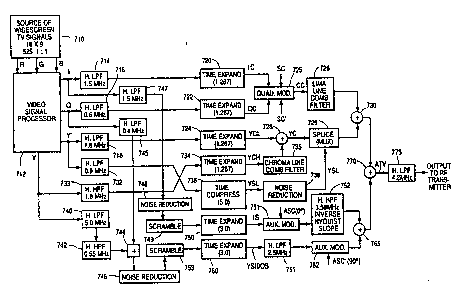
In the NTSC compatible widescreen transmitter/
encoder of FIGURE 7, a widescreen television signal source 710,
2 5 such as a color television camera, provides a 16x9 wide aspect
ratio 1:1 progressively scanned (non-inlerlaced) television signal
with color components R, C and B, These signals are processed by
a ~ideo signal processor 712 to provide luminance outpul signals
Y, Y' and color difference OUlpUI signals I and Q, Processor 712
3 0 includes circuils for translating tl)e R, G, B input signals ~o 1, Q, Y
formal, vertical-temporal fillers for pre-filtering each of the 1, Q, Y
signals, and progressive scan lo inlerlaced scan converlers for
each of Itle 1, Q, Y signals, Oulput signals 1, Q and Y from processor
712 are 262 line progressive scan signals, An OUlpUI signal Y' is a
~, 3 5 525 line inlerlaced luminance signal.
Encoding of Ihe main (i,e,, "center") panel informalion
will be discussed firsl, Color difference signals 1, Q anLI luminance
.
.
- - , -
. .
.: . - - , .
. ~ . .
wO 92~08318 ~ 3 ~ ., PCr/US9l/07l79
- I 2 -
signal Y from unil 712 are respeclively fillered by fillers 714
716 and 718 before being lime expanded by unils 720 722 and
724 respeclively. Unils 720 722 and 724 exhibil a lime
expansion faclor of 1.267 and operale only on Ihe cenler (mailI)
panel porlion of Ille l Q Y signals from fillers 714 716 and 718.
Thus lime expanders 720 an~J 722 respecli~ely provide ou~pul
cenler panel color difference signals IC and QC. Time expander
724 provides al~ oulpul lurninance cen~er panel low frequency
sign~l YCL. Signals IC anll QC qua(lra~ure modulate 3.58 MHz
1 0 quadralure pbasell subcarriers SC and SC in a modulalor 725 to
produce a mo~lulaled cenler panel chrominallce signal CC. This
signal is processe(3 by a luminance line comb filler 726 lo remove
luminance informalion before being applie~J lo a center panel .
chrominance ~inpul`` of an adder 730.
1 5
TlIe cenler panel luminance signal input lo adder 730
is developed as follows. The Y luminance signal from processor
712 is high pass fillered by a unit 733 and lime expanded by a
unil 734 WhiCIl operales only during Ihe cenler panel inlerval to
develop a cenler p~nel higlI frequency luminance signal YCH. rhis
signal is processed by a chrominance line comb filler 735 to
remove cnrominance informalion before being combined will~
conler p~nel low frequency luminance signal YCL in adder 728 lo
produce a cenler panel luminance signal YC.
. 25
Expanded cenler panel luminance signal YC is spliced
Io cornpressed sille panel low fre~uency lurninance inforlllalion
YSL by moans of a mulliplexer 725~. Briefly as discussed in de~ail
in U.S. palen~ 4,855,811 - Isnardi, signal YSL conslilules lime
. 30 compressed low frequency lefl and righl side panel luminance
informalion wllicll is pl~ced in left anl) rigllt horizolltal overscan
regions of Ihe cen~er panel signal by means of mulliplexer 729.
Signal YSL is oblailled by til~ering signal Y from processor 712 by
means of a 0.8 M~lz horizonlal low pass filler 732 Illen selectively
lime compressing Ihe side panel porlions of Ihe fillered signal by
means of a compressor 736 whicll operales only ~Juring Ille side
panel inlervals~ Signal YSL from compressor 736 is processe~ by
a noise reduclion unil 738 for improving Ille siglIal-~o-noise
.
.
wo 92/083~x 2 0 9 1 7 2 t, Pcr/US91/07179
- I 3 -
characlerislic of signal YSL before being applie~ lo splicer 729.
The oulput of mulliplexer/splicer 729 is applied lo Ihe luminance
inpul of cenler panel signal combiner 730. Noise reduclion uni
738, as well as noise reduclion unils 746 and 748, are amplilude
5 compansion unilS having similar complemenlary counlerpart unilS
wilh inverse operaling characleristics at a receiYer.
High frequency side panel informalion is processed as
follows. The "I" color difference componenl from processor ~I'7 is
10 fillered by a I.5 MHz low pass filler 747 lo produce a wideband I
signal, and is prbcessed by noise reduction llnit 748. Tlle OUtpUI
signal from unit 748 can be processed by a scrambling nelworl~
749 of lhe Iype shown in FIGURE 2 before being time expandeLI
by unit 750. The oulpul signal from unil 748 is time expanded
I S during side panel inlervals by a lime expander 750 lo produce
wideband side panel color difference component IS. This signal is
applied to an auxiliary modulalor 751 for amplilude modulaling
an auxiliary subcarrier ASC wilh a nominal 0 phase. Subcarrier
ASC exhibils illustralively a frequency of 3.58 MHz, Ihe frequency
2 0 of Ihe standard chrominance subsarrier, bul exhibils a phase
which inverls from field-lo-field unlike Ihe slandard chrominance
subcarrier. Specifically, Ihe phase of signal ASC inverls every 262
horizontal lines (262H).
.: .
2 5 The modulaled signal from unil 751 is applied to a
3.58 MHz horizontal high pass filter 752 having an inverse
Nyquist slope. Filter 752 mirrors a filler al a receiver having a
Nyquist slope to achieve a desired amplitude response al a
receiver demodulator. Specifically, lhe cascade of inverse Nyquis~
3 0 slope filler 752 al Ihe encoder wilh a complemenlary Nyquist
slope filler at a receiver decoder produces a desired flat
amplitude response for high frequency side panel luminance
signal YSH when demodulaled al lhe receiver. SUCII cascade of
Nyquist slope filters also assures lhal modulaled auxiliary
3 5 subcarrier ASC exhibils symmetrical double sideband IS
information so thal proper quadralure demodulation is achieved
al Ihe decoder, i.e., so Ihal signal IS mainlains a desired phase
characlerislic and does nol crosslal~ inlo componenls YSH or QS.
/
.
.
wo 92/08318 ~ ~ ~ 7 ', 3 Pcr/US91/07179
- I 4 -
Side panel high frequency luminance informalion and
side panel color difference component Q are combined for
processing. Tlle Q oulput signal from processor 712 is conveyed
via a 0.4 MHz horizonlal low pass filler 745 lo a combiner 744
where il is combined with signal Y from unit 712 after fi~lering by
a 5.0 MHz horizontal low pass filler 740 and a 0.55 MHz horizontal
high pass filler 742. The oulpul signal from combiner 744 is
processed by noise reduction unit 746 and aflerwards time
expanded by a unit 760. The output signal from unit 746 is
processed by a scrambling network 753 of lhe type shown in
l:IGURE 2 before being lime expanded by unit 760. Expander unil
760 operates during the side panel in~ervals for producing -
combined si-~e panel llighs signal YSH/QS, i.e. side panel hi~
frequency luminance informalion combine(l wilh side panel Q
color difference information. Because time expander 760 is nol
ideal low energy repea~l speclra are generated above 2.5 MHz.
Low pass fil~er 761 removes lhese repeat speclra and: prevents
them from cross-lalking inlo lhe main (cenler) panel componenl
2 0 afler modulalion.
Combined signal YSH/I~S is coupled Yia a 2.5 MHz
horizonlaJ low pass filter 761 ~o an auxiliary modulator 762
which modula~es an auxiliary 3.58 MHz subcarrier ASC willl the
oulput signal from filter 761 Subcarrier ASC is in phase
quadralure witll subcarrier ASC and exhi~i~s a similar pl~ase
inversion from field to field. The oulput signal from modulator
762 and lhe oulpul signal from filter 752 are combined by an
adder 765. An adder 770 combines tlle outpul signals from
3 0 adders 730 and 765 lo produce a compatible widescreen
advanced lelevision signal ATV. This signal is low pass filtered by
a 4.2 M~Jz filler 775 lo reslrict signal ATV lo lhe slandard NTSC . t
channel bandwidlll before being applied lo an RF lransmitler for
broadcasl. j
The disclosed scrambling apparalus also can be
inserted belween lhe lime translalion and modulalion unils i.e.
belween blocks 750 and 751 and belween blocks 760 and 762 in
.
.. : . -
wo 92/08318 2 0 9 ~ 7 2 3 Pcr/us91/n7l79
-15
FIGURE 7, Alternatively, Ihe scrambling apparatus can be
inserted after each of modulalor blocks 751 and 762 for
scrambling the modulalcd auxiliary subcarrier, or a single
scrambling unit can be used afler combiner 765, Corresponding
S allernative locations are used for unscrambling unils al the
decoder, e,g" between units 842 and 844 and between units 854
and 856, or prior lo auxiliary subcarrier demodulator 852 in
PIGURE 8,
FIGURE 8 shows a portion of a widescreen television
receiver including apparatus for decoding Ihe widescreen ATV
signal generaled ~y lhe arrangement of FICURE 7. A receive(J
baseband encoded ATV signal (e,g" from an RF tuner and
demodulator assembly not shown) is applied to a 1,6 MHz
15 horizontal high pass filter 8 1 0, the outpul of which is applied to
an intraframe processor 812, Processor 812 averages (additively
combines) and differences (subtractively combines) image lines
262H apar~ within frames above 1,6 MHz to recover high
frequency main panel signal information al an output AVG.
2 0 Modulaled side panel high frequency information is provided at a
differencing outpul DIFF of processor 812.
The main panel component from the AVG output of
' processor 812 is ~iltered by a horizontal line comb filter 814 to
2 5 provide separated luminance (Y) and chromioance (C~ OUlpUt
components, The sepa!ated main panel luminance component is
time compressed by a unit 820, whicll operates only during the
main panel interval, lo reslore separated main panel component Y
Io its original spalial relalionship, Tbe lime compressed signal
3 0 from unil 820 is Ihen fillered by ~ 5,0 MHz horizontal low pass
filler 822 lo develop main (center) panel luminance high
frequency componenl YCH. The separa~ed main panel
chrominance information (C) is quadra~ure demodulated by a
demodulator 815 responsive lo quadralure phased reference
35 signals SC and SC' having Ille fre4uency and phase characteristics
of corresponding subcarrier signals provided at Ille
encoderllransmilter~ Demodulaled cenler panel I and Q color
difference componenls IC and QC are horizonlally low pass fillered
:. .
. .
.
wo 92/08318 . 2 0 ~ Pcr/us91/07l79
- I 6 -
by fillers 816 and 818 respecli~ely before being lime compressed
by unils 817 and 819, Time compression unils 817 and 819
operale during Ihe center panel inlervals lo restore Ihe original
spatial relalionship of signals IC and QC,
The center panel low frequency luminance informalion
is restored lo ils original form by means of fiîter 825 and lime f
compressor 828. Horizonlal low pass filler 825 passes frequencies
of input signal ATV which are below aboul 1.6 MHz lo lime
10 compressor 828, which operales during lhe cenler panel interval
to restore low frequency cenler panel luminance information tc ilS
original spali~l relationship, as signal YCL.
The inpul ATV signal is also applied lo a noise
15 reduction uni~ 830, which exhibits Ihe complementary operating
characteristics of unit 738 in Ihe encoder of FIGURE 7. A lime
expander 832 operales during Ihe side panel inler~als lo reSlOre
Ihe original spalial formal of ~he side panel informatio~ which had
been time compressed and placed in llle horizonlal overscan
20 regions. The OUlpUl signaî from expander 832 is processed by a
0.8 MHz horizontal low pass fil~er 834 ~o provide low frequency
side panel luminance signal YSL in i~s original spalial form.
To recover side panel I color difference componenl IS,
25 lhe sigllal from Ihe DIFF oulpul of processor 812 is demodulaled
by an auxiliary demodulalor 840 which responds lo an auxiliary
reference signal ASC h~ving thc same frequency and phase
characlerislics as subcarrier ASC developed al Ihe encoder, The
demodulaled signal from unil 840 is fillered by a 1,0 MHz
3 () horizonlal low pass filler 842, lime compressed during side panel
inlervals by a uni~ 844 lo reslore lhe original spalial formal of lhe
signal componenl, and processed by a noise reduclion unit 846 lo
produce side panel color I difference componenl IS, Noise
reduction unit 846 and unit 748 al lhe encoder exhibit
3 5 complemenlary operating characlerislics, The OUlpUt signal froro
time compressor 844 is processed by an unscrambling networl;
845 of the type shown in FICURE 4 before being processed by
noise reduction unit 846.
-- .
'
WO 92~08318 PCT/US91/07179
`20'~723
-17-
To recover side pànel components YSH and QS, tlle
signal from tlle DIFF oulpul of processor 812 is processed by a
3.58 MHz horizolllal low pass Nyquist slope filler 850 before being
5 demodula~ed by auxiliary demodulalor 852. Wi~h regard lo lhe
use of Nyquisl filler 850 it is noled lhat in this example
component QS is a double sideband signal modulation colnponent
of auxiliary subcarrier ASC' occupying 3.38 MHz to 3.79 MHz, all~l
componenl YSH is a (lower) single sideband modulation
I U componenl of auxiliary subcarrier ASC' occupying 1.78 ~IHz to
3.25 MHz Imparling a Nyquist slope to lhe higher energy (louble
sideban~J region of the combined YSH/QS modulaled signal (fronl
3.08 MHz lo 4.U8 MHz) reduces Ihe effective energy of the double
sideband region by one-half, so lhat a flat demodulation
I S amplitude response results over lhe auxiliary subcarrier
modulalion frequencies. Demodulator 85~ also responds to an
auxiliary re~erence signal ASC' having lhe same frequellcy and
phase characleristics as au~iliary subcarrier ASC' developed at lhe
encoder. A demodulated oulpul signal from demodulator 852
2 0 contains combined YSH and QS components and is filtered by a 2.5
MHz horizontal low pass filter 854.
The oulpul signal from filter 854 is time compressed
by a unit 856 which operates during side paneJ intervals to
Z 5 restore the original spatial relationship of lhe combined YSH/QS
side panel informalion. The time compressed signal is processe(3
by a noise reduction unit 858, whicll exhibits the complernentary
operating characteristics of unil 746 in the encoder system of
F1~3URE 7. The outpul signal from time compressor 856 is
3 0 processed by an unscrambling nelwork 857 of the type showll in
FICURE 4 before being processed by noise reduc~ion unit 858. The
oulpu~ signal rrom noise reduction unil 858 is separatell inlo llle
YSH and QS compollenls by means of a 0.55 MHz horizonlal higi
pass filler 860, and a 0.4 MHz horizonlal low pass filler 861,
3 5 respectively.
The output signals developes3 by the decoder
apparalus Or FIGURE 8 are processed further as shown in FIGURE
wo 92/08318 ~ PCr/US91/07179
- I 8-
g. Signals IC ~ntl IS, QC auul QS, YCII anli YSII, and YCL and YSL nre
respeclively spliced by splicers 921, 922, 923 and 924
` ~ respeclively. Oulpul signals rrom splicers 923 and ~24 are
combine(l by an adder Y26 ~o pro~iLle a reslored wi(lescreell
- 5 iulnillallce signal will~ Illain panel and side pallel inforlnalioll. l lle
widescreell cllrolllinallce signals from splicers 921 al~ i 922 an(l
Ille widescreell lunlinance signal froln adder 926 are con-~erled
froln inlerlaced to progressive scan ~orlnal by me~lls of
couverters ~3()-SJ32 l~efore being converled lo analog fornl via a
I () digilal-lo-analog converler uuil ~35. Widescreen analog signals 1,
Q, Y are ulalri~eLI anlJ processed by convenlional video signal
processing circuils in a nelwork 938 lo pro~luce color image
represenlalive signsls R, a and B suilable for display l)y a
widescreen image reproducing device Y~0.
I 5
FIGURE 10 depicls apparalus suilable ror generaling
quadralure pllased signals SC anll SC', and quadralure phased
au~iîiary signals ASC and ASC'. A signal generalor lOIt) provides,
ror e~ample, a 3.58 M11z sinusoidal signal SC at a nominal 0
pllaSe. Tllis 5igll81 iS pllaSe Shifled 90 by a ne~work 1012 lo
produce signal SC'. Signal ASC is derived frolll signal SC by means
of a field pllflse conlrol unil 1014, wllicll produces auxllisry signal
ASC willl a phsse 11l8l reverses froln riel-J lo fielll relative lo Ille
phase of a slandard chrominance subc~rrier. A 90 phase shifler
2 5 1015 ptoduces au~lliary signal ASC' in phase quadralure will
auxlliary signal ASC.
::
'
,,
- -
. ~ ' ' .