Note: Descriptions are shown in the official language in which they were submitted.
W092/07680 P~T/US91/07191
~9'~32~
THICK METAL MICROWAVE SUSCEPTOR
BACKGROUND OF THE INVENTION
Heating of foods in a microwave oven differs
significantly from heating foods in a conventional oven.
In a conventional oven, heat energy is applied to the
exterior surface of the food and moves inward until the
food is cooked. Thus, food cooked conventionally is
typically hot on the outer surfaces and warm in the
center.
Microwave cooking, on the other hand, involves
absorption, by the food, of microwaves which
characteristically penetrate far deeper into the food
than does infrared (heat). Also, in microwave coo~ing,
the air temperature in the microwave oven may be
relatively low. Therefore, it is not uncommon for food
cooked in a microwave oven to be cool on the surfaces
and much hotter in the center. This makes it difficult
to brown food and make it crisp. Therefore, it is
d~fficult tD make some food cooked in a microwave oven
aesthetically pleasing.
In order to facilitate browning and crisping
of food in a microwave oven, devices known as susceptors
have been developed. Susceptors are devices which, when
exposed to microwave energy, become very hot. By
placing a susceptor next to a food product in a
m.icrowave oven, the surface of the food product exposed
to the susceptor is surface heated by the susceptor and
thereby becomes crisp and brown.
Many conventional susceptor structures have
included a thin metal film, typically 60 - l00A of
Aluminum, deposited on a substrate such as polyester.
The metali7ed layer of polyester is typically bonded,
,
W092/07680 PCT/~S91/07191
:2~'32'~
--2
for support, to a support member such as a sheet of
paper board or corrugated paper.
Conventional susceptors have certain
drawbacks. They undergo a process called breakup in
which the electrical continuity o~ the thin metal film
is lost during cooking. This is; described in more
detail in the Wendt et al U.S. Patent No. 4,927,g9l.
The result of the loss of electrical continuity is an
irreversible loss in the susceptor's microwave
responsiveness and a lower level of percent power
absorption in the susceptor during cooking. Lower power
absorption leads to lower susceptor cooking temperatures
and a corresponding decrease in the susceptor's ability
to crisp food.
In order to further discuss the relevance of
this deterioration, some other relationships should be
set forth. The complex dielectric constant ~ of a
material is defined as follows:
1: ~O~r Eo (~r i ~r ) Eq.
where ~0 is the permitivity of free space,
8.854 x lO~l4Farads/cm;
~r is the complex relative dielectric constant
, of the susceptor, relative to free space;
! ~ Er~ is the real part of the complex relative
dielectric constant ~ r; and
~ r~ ~ is the imaginary part of the comple~
relative dielectric constant ~r. ~r' ' is also known as
thP loss factor for the material.
As an example of conventional susceptor
operation, a frozen food product could be placed on a
susceptor. The susceptor and the food product could
W092/0~80 pCT/~'~91/07191
2~9~;~2~
then be subjected to microwave energy. Since ~r~ ~ (the
imaginary part of the complex relative dielectric
constant) of ice is very low, the frozen food product is
initially a poor absorber of microwave energy.
Therefore, the susceptor absorbs an excessive amount of
the microwave energy and begins to deteriorate.
Meanwhile, the frozen food product absorbs very little
energy. This is undesirable. As the frozen food
product thaws and starts absorbing microwave energy, the
ability of the susceptor to absorb energy, and thereby
surface heat the frozen food product, has already been
deteriorated. Since this deterioration (i.e., the
change in the electrical continuity of the susceptor) is
generally irreversible, the susceptor is incapable of
properly browning and crisping the food product.
Xn addition, as the susceptor deteriorates, it
heats in a non-uniform fashion resulting in hot spots
distributed along the surface of the susceptor. This
results in uneven surface heating of the food products.
Further, as the susceptor deteriorates and the
microwave transmissiveness of the susceptor increases,
the food product may be subjected to an undesirable
amount of dielectric heating. This can cause the food
product to become tough or to attain other similarly
unappealing qua.lities.
Therefore, there is a continuing need for the
development of susceptor structures which are not
plagued by the problems of thin metallic fllm-type
susceptor structures.
SUMMA~Y OF THE INVENTIQN
The present invention is a microwave susceptor
structure having a thick metal layer and a matching
layer coupled to the thick metal layer. The matching
'-", ' : "
,:
' ~
W092/07680 PCTIUS91/07191
-' 2~32~
layer couples a desired amount of power into the thick
metal layer.
BRIEF DESCRIPTION OF THE DRAWINGS
FIG. l is a drawing of the susceptor structure
of the present invention.
FIG. 2 is a graph showing percent power
absorbed plotted against dielectric thickness for
dielectric material and metal of the susceptor shown in
FIG. l.
FIG. 3A shows a three dimensional plot of
percent power absorbed by a first embodi~ent of a
susceptor of the present invention.
FIG. 3B shows a three dimensional plot of
percent power absorbed by a second embodiment of a
susceptor of the present invention.
FIG. 4 is a graph showing percent power
absorbed plotted against dielectric thickness.
DETAILED DESCRIPTION OF THE PREFERRED EMBODIMENTS
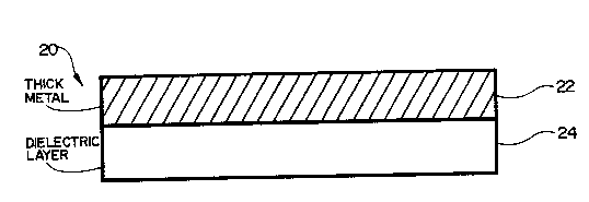
FIG. l shows a susceptor 20 of the present
inventio~. The susceptor 20 includes an electrically
thick (greater than approximately 3 skin depths thick)
metal layer 22 and an impedance matching dielectric
layer 24. The metal layer 22 is typically bonded to
layer 24 such that food, when placed on the thick metal
layer 22, is isolated from any chemicals or other
~m~terials in layer 24.
Until now, it has generally been thought that
thicX metals would not make good susceptor structures
since they have high electrical conductivity. Indeed,
the thick me~al portion 22 of the invented sus~eptor 20
will not heat significantly without the impedance
matching dielectric layer 24.
W092/07680 ~CT/US91/07191
2 ~ 2 ~
In the present inventionl the interaction of
the susceptor with the microwaves provided by the
microwave oven is viewed as a transverse electromagnetic
(TEM) plane wave which propagates within the microwave
oven. Hence, by choosing the proper dielectric layer
24, a desired amount of power can be coupled into thick
metal layer 22. In other words, dielectric layer 24 is
used as a matching layer for matching the wave impedance
of the plane wave, as defined by the medium of
transmission, generated by the microwave oven to that of
the thick metal layer 22. By "matching", it is meant
that the overall reflection coefficient of the
dielectric and thick metal composite is reduced or
eliminated and the power absorbed by the thick metal
layer 22 is increased.
The wave impedance (Z) of the microwave is
related to the characteristics of the wave front and the
medium of transmission by the following relationship:
Eq. 2
Z - ~
Where the medium of transmission is air, the
wave impedance (Z0) is substantially represented as:
Eq. 3
zO ~ 377 n
By matching the impedance of the thick metal
layer 22 with the wave impedance of the microwaves in
the microwave oven, a desired amount of power is coupled
. . . . .
W092/07680 PCT/US91/07~1
2 ~ 9 ~ ~ 2 ~
into the thick metal layer 22 and absorbed by susceptor
20. Thus, thick metal layer 22 heats when exposed to
microwave energy.
To couple a -~;~um amount of power into the
thick metal layer 22, quarter wave matching is used. In
other words, for ~iri~ing power transfer,
Eq. 4
Zm~ ~ch ~/ZO Zme ~a1
where Zmat~h is the impedance of dielectric
layer 24;
ZO is the characteristic impedance of free
space, and
Zmetal is the impedance of the thick metal
layer 22.
The thickness (d) of dielectric layer 22 is
chosen as:
Eq. 5
d~ h
where Amatch is the wavelength o~ the
microwave in the matching layer 24. Thus, by choosing
a ~ielectric layer 24 which has an appropriate relative
dielectric constant ~r and an appropriate thickness (d),
the amount of power coupled into a metal layer 22 having
a given electrical conductivity (a) can be ~imj zed.
It has been seen that, when metal layer 22 is
formed of a thick metal such as aluminum fvil, and when
dielectric layer 24 is formed of a high dielectric
material (e.g. a commercially available metal loaded
W092/~7680 PCT/US91/07191
polymer similar to that disclosed in EP0 Publication No.
242,952 to E.I. DuPont De Nemours & Co.) the amount of
power absorbed during microwave heating is related to
the thickness of the dielectric layer 24 as shown in
FIG. 2. FIG. 2 shows a graph calculated from a computer
model of the thickness of ihe dielectric material 24
plotted against the calculated percent absorbed power by
susceptor 20 during microwave heating. FIG. 2 shows
that a great percentage of the system power can be
absorbed by susceptor 20 if metal layer 22 and
dielectric layer 24 are chosen properly.
Computer simulations have been run in whlch
the thickness of the dielectric layer 24 and the complex
dielectric constant o~ the dielectric layer 24 were
systematically varied. For example, in one case, the
thickness of the dielectric layer 24 was varied from
approximately 0.16 cm to 0.006 cm in approximately 50
steps. In addition, the complex relative dielectric
constant of dielectric layer 24 was varied from 500-jo
to 2000-jO in approximately 50 steps. It was assumed
that metal layer 22 was aluminum with an electrical
conductivity of 3.5 x 10⁵/ ohm cm. The maximum system
power absorbed was 28.4~. A three dimensional plot of
the percent power absorbed by susceptor 20 plotted
against the dielectric thickness and the complex
r~lative dielectric constant of dielectric layer 24 used
in the computer simulations is shown in FIG. 3A.
Surprisingly, it has also been shown that,
where the metal layer 22 is a poor conductor, more
microwave power is absorbed by susceptor 20 than if the
metal layer is a good conductor. For example, another
computer simulation was run using a dielectric material
having a complex relative dielectric constant varying
. .
Wo~/07680 Pcr/us9l~o7l9l
from 500-jO to 2000-jo in approximately 50 steps. In
addition, the simulation included metal layer 22
comprising Nichrome, having an electrical conductivity
of 104/ohm cm. A three dimension2l1 plot showing the
percent power absorbed by susceptor 20 using Nichrome
plotted against the dielectric thickness and the complex
relative dielectric constant of dielectric layer 24 is
shown in FIG. 3B. The maximum power absorbed by
susceptor 20 in this second case was 91.8%.
Thus, by choosing the dielectric layer 24 with
an appropriate thi~kne~s and complex relative dielectric
constant 50 that the impedance of the thick metal layer
22 is sufficiently matched to the wave impedance of the
microwave generated by the microwave oven, substantially
any desired amount of power can be coupled .into the
thick metal layer 22. By using this impedance matching
te~h~lque, the thick metal is heated and operates
properly as a susceptor in a ~icrowave oYen.
It is worth noting that microwaves generated
in microwave ovens may typically have a frequency of
approximately 2,450 megahertz. Therefore, the desired
amount of power can be coupled into the thick metal
layer 22 by carefully choosing the impedance of
susceptor 20 to match (or match sufficiently to couple
the desired amount of power), the wave impedance of a
.~microwave (typically modeled as a plane wave) at a
frequency of 2,450 megahertz to the impedance of the
thick metal layer 22.
Also, although the value of the dielectric
loss factor, E~ll, of the dielectric layer 24 is not
critical, it should generally be as small as possible.
If ~rl' of the dielectric layer 24 is too large, the
W092/~7680 PCT/U~91/07~91
2 0 ~
dielectric layer 24 may heat excessively and, in certain
cases, deteriorate.
It has also been noted that, in using
susceptor structure 20 of the present invention, a
certain amount of temperature control is possible. FIG.
4 shows a graph of dielectric thickness of dielectric
layer 24 plotted against percent power absorption by
susceptor 20. A dielectric material is chosen where the
dielectric constant is temperature dependent. For
example, as shown in FIG. 4, at a dielectric thickness
of 0.092 cm, the real portion of the complex relative
dielectric constant is 1000 when little or no microwave
energy has been absorbed by susceptor 20 (i.e., when
susceptor 20 is cold). At that point, the percent
absorption capability of susceptor 20 is 40%. However,
as susceptor 20 absorbs microwave energy and heats, the
dielectric constant drops to 800 and the percent of
system power absorbed by susceptor 20 is reduced to
approximately 5%.
In otAer words, FIG. 4 shows two graphs where
the dielectric constant shifts as the dielectric layer
24 heats. Initially, dielectric layer 24 heats very
rapidly (40% absorption) and when it reaches a given
temperature, its percent absorption drops to
approximately 5% (the heater turns off~. Thus, by using
a proper dielectric material, one with a temperature
dependent relative dielectric constant, temperature
control can be achieved.
I~ one preferred em~odiment, the high
dielectric material layer 24 is Barium Titanate or
Calcium Titanate. In another preferred embodiment, it
is a metal flake artificial dielectric or any other high
~ material.
WO 92/07680 P~/~JS91/Q7191
--10--
CONCLUS I ON
By using the susceptor structure of susceptor
20, a surface heating susceptor can be achleved which
cooks, in essence, like a frying pan. The heating is
accomplished by currents within the metal layer 22, and
metal layer 22 is highly arc resistent.
Also, the metal layer 22 electrically isolates
the food from the dielectric layer 24. Thus, the
electric field standing wave pattern inside the food
remains relatively constant, unaffected by changes in
the susceptor 20. The isolation provided by metal layer
22 also prevents contamination of the food product by
any chemicals in the dielectric layer.
Further, the dielectric layer 24 can be chosen
with a dielectric constant which i5 temperature
dependent. This allows temperature control to be
achieved.
Although the present invention has been
described with reference to preferred ,embodiments,
workers skilled in the art will recognize that changes
may be made in form and detail without departing from
the spirit and scope of the invention.