Note: Descriptions are shown in the official language in which they were submitted.
2095656
MOLDED PLASTIC MICROWAVE ANTENNA
CROSS REFERENCE TO RELATED PATENTS
Reference is made to copending U.S. Patent No. 5,398,010 entitled
"Molded Waveguide Components" and U.S. Patent No. 5,380,386 entitled
"Molded Metallized Plastic Microwave Components and Process for
Manufacture" .
BACKGROUND
The present invention relates generally to microwave antennas, and
more particularly, to microwave antennas that are made of molded plastic
0 material.
Conventional microwave antennas are generally made of metal
components, and typically include an antenna aperture and electromechanical
phase shifter, a horizontal feed network, a plurality of interconnecting
waveguides, a vertical feed network including conventional rotary field phase
shifters, and a sum and difference monopulse feed network. In general, all
of these components have heretofore been fabricated out of metal. This
results in a costly and heavy antenna system.
The two U.S. patents noted above address methods for manufacturing
certain components employed in the present invention the fabrication of
2 o detailed components used to complete a molded metallized thermoplastic
antenna in accordance with the present invention. Furthermore, U.S. Patent
No. 4,499,157, entitled "Solderable Plated Plastic Components and
Processes for Manufacture and Soldering" assigned to the assignee of the
present invention addresses fabrication of certain antenna components by
2 5 soldering plated plastic components.
It is therefore an objective of an aspect of the present invention to
provide for a microwave antenna wherein substantially all antenna
components are fabricated from molded or extruded, plated, plastic
components.
-2- 2ng5~56
SUMMARY OF THE INVENTION
In order to achieve the above objective, the present invention, in one
aspect thereof, comprises a microwave radar antenna that substantially
comprises molded or extruded thermoplastic components that are assembled
into completed assemblies, are then metallized by either electroless or
electroplated with copper to achieve RF conductivity. The finished
subassemblies are joined together forming a completed microwave radar
antenna.
0 The molded metallized plastic antenna uses a thermoplastic material,
such as polyetherimide, Ultem 2300TM or Ultem 23l0TM, or any suitable high
strength, high temperature thermoplastic that is used to injection mold or
extrude detailed microwave components. The molded components are
assembled, using epoxy adhesives, solvents or any suitable mechanical
methods into microwave subassemblies. These subassemblies are then either
electroless copper plated or electroplated to provide RF conductivity. The
metallized subassemblies are then joined together using mechanical methods
to form a completed radar antenna, replacing heavier more costly metal
radar antenna components.
2 o The molded met~lli7ed plastic antenna is comprised of an antenna
aperture and electromechanical phase shifter section, a centerfeed section
comprising a horizontal feed network, interconnecting waveguides, a vertical
feed network including conventional rotary field phase shifters, and a sum
and difference monopulse feed network. The antenna also includes a
2 5 conventional beam steering controller that provides electronic antenna beam
steering and a power supply.
Z0956~6
- 2a -
Other aspects of this invention are as follows:
In an antenna cuLuplising an ~7imuth phase shifter assembly comprising a
plurality of waveguides and an antenna ape.lule, a ce,.l~rc~d waveguide accembly that
forms a hnn7nntal feed network that is coupled to the a7iml-th phase shifter assembly; a
plurality of ultcl~;onne~ !;ng waveguides fabricated from molded plastic and
~ubse~3ue.llly metalli7~A lcj~c~i~ely coupl~d to individual ones of the plurality of
ce..ltlr~l waveguide assemblies of the cenu.r~d waveguide acsombly; a plurality of
10 rotary field phase shifters coupled to individual ones of the plurality of illle.c~ln~Ling
waveguides; a pluralit,v of ver~cal feed networks couplçA to selected ones of the
plurality of rotary field phase shifters that are fabricat~A. from lded plastic and
subsequently m~t~lli7~A; and a sum and dirr. .~ ce Luono~ulse feed network having an
input port that is coupled to the plurality of vertical feed mlwc,ll~s, the improvement
CoLu~ g:
an a,;.~ h phase shifter acc~mbly fahri~teA~ from a plurality of molded plastic
waveguide portions that are molded and sub~uently m.-talli7eA
A molded, m~t~lli7~A plastic microwave arltenna comr.cing:
an a7imllth phase shifter acsçmbly fabricated from a plurality of molded plasticwaveguide portions that are molded and subsequently m~talli7~A, and wherein the
plurality of molded plastic waveg ude portions are mated and stacked together to forrn a
pluralily of waveguides, the a7imllth phase shifter a sembly forming an ~nt~onn~
ap~l Lul ~,
a centerfeed waveguide acsemhly that forms a holiLonlal feed network that is
coupled tO the a7imnth phase shifter ac~mhly and which c~m~ eS a plurality of
molded plastic c~ reed waveguide acs~omhli~s whose CO...pOI ~n~ are fahricated from
molded plastic and subsequ~ntly m~-~lli7~A _nd wherein the plurality of molded plastic
centerfeed waveguide assemblies are mated and stacked together to form the holizollL~l
feed networlc;
;c~
..~ .,
20956~6
- 2b -
S a plu~ality of interu~nn~ing waveguides fahnc~ted from molded plastic and
subse~luenlly m~talli7e~ respectively coupled to individual ones of the plurality of
ce.,~.recd waveguide assemblies of the centerfeed waveguide acsçmhly;
a plurality of rotary field phase shifte~s coupled to individual ones of the
plurality of i~ ;ng waveguides;
a plurality of vertical feed networks coupled to selecte~l ones of the plurality of
rotary field phase snLfters that are f~ ted from molded plastic and subsequently
m~t~lli7~-
a sum and dirÇc.ence monopulse feed network having an input port that is
fabricated from molded plastic and subsequently m~t~lli7~ coupled to the plurality of
vertical feed networks.
The advantages of molded met~lli7~d plastic ~ntenn~ are many, and include
lower cost, lower weight, better perfoImance, lower m~n~lfa~turing costs, and superior
RF ~.ru~ ,ce. More particularly, injection molded or extruded thermoplastic details
are finished into sub~ccemblies replace individually m~rlline~d usually aluminum or
magnesium, metal ~cspmblies The thermoplastic assembly cost is much less becauseof lower raw m~t~-ri~l cost and a dr~m~tic~lly sl-.,~Lned fabrication time. The metal
details have each feature m~f~hin~ one at a time, where the lL~,.~oplastic details have
them all ciml~lt~neously reproduced during the injection mol~1ing or extruding opera-
2095656
tion. ThermoplQcti~s) which are suitable for this application, are typically 30 to 50%
lighter for a given volume than Qlllminllm This allows the finichfA microwave radar
Qntf nnQ to be lighter, re lucing the total radar set weight. Bonding before plating
reduces the p~lr.J. . . ~Qnce penalty of a possible high loss æcsçmhly joint. The lower
5 m~nnf~r~turing costs reduce in-process scrap costs. The plastic ~ntPnnQ of the present
invention has s~lperior RF pclrollllQn~e when coll,~d~d to similarly m~mlfQ-~tured
Ql.".. ;.. assemblies.
The use of the present microwave Qntf nn~Q~ incc,l~uld~ing molded mf tQlli7P~l
plastic col~lpollents results in an antenna having better ~lÇ.. ~nce, lighter weight, and
10 much lower mQnufQctnring costs. This fQbric ætiQn concept may be applied to new and
existing col.. ~.~;ial and military antenna appli~Qtionc having either the disclosed design
or a flat planar design.
BRIEF DESCRIPTION OF THE DRAWINGS
The various f~Lulcs and advantages of the present invention may be more read-
ily understood with reference to the following df tQilfA description taken in conjunction
with the accoll~ lying drawings, wherein like reference numerals designate like struc-
tu~l elementc, and in which:
Fig. 1 shows a schem~tic diagram of a molded plastic microwave ~ntçnnQ in
20 accordance with the principles of the present invention;
Fig. 2 shows details of the apcllulc section of the Qntf nn~ of Fig. 1;
Fig. 3 shows a molded ce~ lr~,ed waveguide ~csemhly employed in the
antennaofFig. l;
Fig. 4 shows a molded interconnecting waveguide assembly employed in the
25 antennaofFig. l;
Fig. 5 shows a exploded perspective view of a fully Qcsembled in~c~ ",necting
waveguide ~seInhly and centerfeed waveguide slccemhly employed in the ~nt~nn~ ofFig. l; and
Fig. 6 shows an exploded ~ls~;Li..~e view of a completely ~ccemhled micro-
30 wave Qnt~nnQ coll~sponding to the Qntenn~Q of Fig. 1.
DETAILED DESCRIPTION
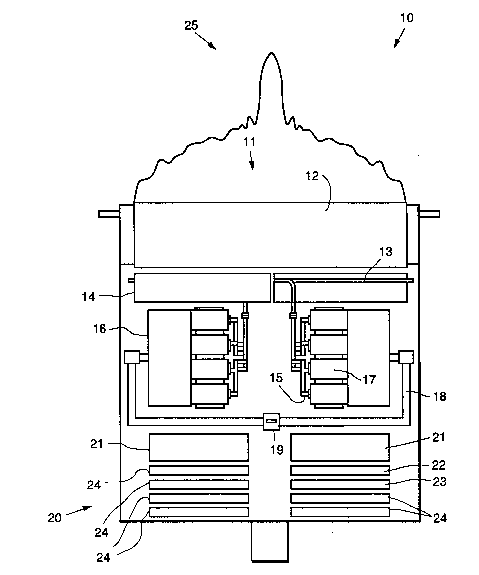
Refernng to the drawing figures, Fig. 1 shows a SChf ~ ;C diagram of amolded, mf tQlli7eA, plastic microwave Qntf nn~ 10 in accordance with the principles of
35 the present invention. The mnk1eA, metQlli7~A, plasdc QntennQ 10 is comprised of an
antenna ap~,-lu,~ 11 and elec~u..~ h phase shif;ter section 12. A center-
fee~ section 13 c~mr~ing a ho. ;~ 1 feed n.,lwul~ 14 is c~nnf~teA to dle ele~ ullle-
2095656
chanical ;~.;."..l~. phase shifter section 12. A plurality of in~,10l-n~ting waveguides
15 (also referred to as waveguide ~sç .~ es 15) are c~n~ eA between the cenl~.rced
section 13 and a plurality of conventional rotary field phase shifters 17. A plurality of
vertical feed nelwull~s 16 are coupled b~L~n the plurality of conventional rotary field
S phase shifters 17 and a sum and dirr~ ce ~onc~ulse feed I~Lwol~ 18. A magic tee
19 provides an input for the antenna 10 that is coupled to the sum and dirrcl~,~ce net-
work 18. Electronics for the antenna 10 is provided and includes a conventional beam
stelonng controller 20 that provides electronic ~nt~nn~ beam ste~Ting, power supplies 21
and voltage regulator n, a plurality of digital elc~;LIw~ics modnles 23 and a plurality of
10 drive electronics modllles 24. An ant~nn~ beam 25 is shown em~n~tin~ from the:~ntt~.nn~ a~~ 11 d~-picting a typical output beam profile provided by the ~ntenn~ 10.
Each of the co~ )onC.lLS of the mol l~l m.ot~lli7~1 plastic microwave ant~.nn~
10 of the present invention are co...~ bl~ to convention~l com~o"e,lLs that are made
solely of ..~h;.~rd or fahri~ated metal. In the present ant~-.nn~ 10, ~ litional support
structure for strengh~ning the molded plastic colll~onc"lLs are employed to provide for
a rigid and stable ~nt~nn~ structure.
The antenn~ 10 is constructed from various sub~tomhlies ~ ntifi~d above that
are f~hrir~t~ se~ tely using various metho~s that will be described below. Fig. 2
shows the ~Lulc 11 and ~7.im~lth phase shifter section 12 of the ~nt~nn~ 10. Thephase shifter section 12 is constructed from eighty-five (85) phase shifter plates 26 that
are injection lded from polyeth~rimi-l~ th~.rmoplastic (IJltem 2300 or 2310, for ex-
ample) and m~t~lli7~1 using either an electroless or an electroplate copper plating pro-
cess. Each of the phase shifter plates 26 comprise one-half of a completed waveguide,
and by stacking and ~ligning the eighty-five (85) plates together, the ~ntenn~ 10 is
formed having eighty-four (84) similar waveguides. These phase shifter plates 26 are
substantially the same as conventional metal phase shifter plates in terms of their design
and operation. However, in the present invention, they are made of molded plastic that
is formed and then plated to provide their RF Ll,.n~ ;ng l,lo~c;lLies.
More particularly, the fini~h~l phase shifter plates 26 are st~ A, aligned, and
clamped together using tensioning rods 27 made from a high strength m~eri~l such as
beryllium copper, for example. A housing or enclosure compricing a cc.lle,.reed frame
28a and an a~c.luuc frame 28b that forms a front cover, both of which are made of
al..,.,;,.."., forexample, along with the t~n~ioningrods 27, and top and bottom actll~t-r
plates 29a, 29b, are employed to secure the eighty-five (85) phase shifter plates 26 to-
35 gether into a solid sllu~lulc. A plurality of convention~l ~.;1ll.ll1l phase shifters 12a are
shown e ~ 1;ng through the phase shifter plates 26. These co~ll~"l~ and opera-
tions col..~ t~ the phase shiftRr section 12 of dle plastic radar ~ntenn~ 10.
s 2095656
One ce-nt~-tfee~ waveguide ~cse ..hly 30 that forms part of the cenl~, reed section
13 is shown in detail in Flg. 3. The c~,.,t~,lreed waveguide assembly 30 is ~csemhled
by bonding a plurality of molded thermoplastic details to~Ll.e., which details include
an input cover 31, a folded slot/transverse wd~,l uide cover 32, an upper transition 33,
S and a lower t~nCition 34. The input cover 31, folded slot/transverse waveguide cover
32, upper transition 33, and lower t~.~ncition 34 are also hereinafter referred to as cen-
terfeed ~semhly coml)one,~ts 30. The c~ ree~ waveguide assembly 30 is assembled
using the molded details by bonding, and finiched lim.o-ncions of the bonded unit are
such that the ~ss~ombly 30 is thereafter electlrless copper plated, recl lting in final
10 overall desired limencions.
The bonding operation uses epoxy adhesive 35 to join the input cover 31,
folded slot/llal.s~erse waveguide cover 32, upper tr~ncition 33 and lower transition 34
together. The bond lines be~ ,.,n each of the c.,..t~lreed assembly colll~onents 30 and
the location of the epoxy adhesive 35 (represented by aT~cws 35 in Fig. 3). The center-
feed ~cc~mbly ccll~on~'lLs 30 are typically ~signe~ so that the molded details self-
locate, aiding in the assembly operation. A bonding fixture (not shown) is used to
apply cl~mping p~ ; to the cenl~lr~ csçmbly colll~)ol e,lL~. 30, while the epoxyadhes*e 35 is cured at about 300 F for about 45 ~I~;n~ s After bonding, the bonding
fixture is r~ ccemhled and the c~-~Lelreed waveguide ~csemhly 30 has its cIitical flange
s~ ces 37 finish ~ inY1 Once critical flange 7,,~11 r~CeS 37 have been ~ lly
machined to meet l~ui~lllclll~., the fully ~cc~mhl~ c~l~t~,lreed waveguide ~csembly 30
is ready for electroless copper plating. This plating process is typically an electroless
copper plating process adapted for Ultem 2300 or 2310 IL~lllloplastic.
The electroless copper plating process helps to make the present invention
unique. The electroless copper plating is applied to the finiche~ microwave waveguide
assembly 30 subsequent to fabrication. This process allows complex cc.llll,onents, like
the c~nlelreed waveguide assembly 30, to be plated after ~ccemhly. This removes the
problems associated with using a secondary conductive method (as in conventionalsoldering processes) to make the final assembly and align the critical flange surfaces
37.
With l~L,l."~ce to Fig. 4, a ~ e view of an il~ ;o~ ;..g waveguide 15
(or interco~-n~ -g waveguide assembly 15) is shown in detail, and it comprises an
assembly similar to the cenlelr~,ed waveguide ~c~-..hly 30, but is much simpler in de-
sign and construction. There are four config~ tions of the i~ col-necting waveguide
3S assembly 15 and each confi~ a~ion is molded in two halves and assembled. Fig. 4
shows two such halves of one such configuration, con~ricing a base 41 and a cover
42. The base 41 and cover 42 are also h~ iinar~l referred to as in~l~;onl~ec~ing
`- 2095656
waveguide as~.e,l,~ly cc~ onel.b 40. The base 41 is shown as a U-shaped member
having a sidewall 43 and a plurality of edgewalls 44 c.~.u~c~ g the sidewall 43 to fo
a U-shaped cavity 45. The cover 42 is also shown as a U-shaped 1ll.,lll~, that is
adapted to mate with the base 41, and has a sidewall 46 and a plurality of edgewalls 47
S contarting the sidewall 46.
The int~ ;onnecting waveguide ~c~ .-hly 15 is asse~bl^~ by bonding the two
molded halves comI~ricing the base 41 and the cover 42 together. The bonding opera-
tion uses the one CO~Ol~nt epoxy adhesive 35 to join the base 41 and cover 42
together. These co,..por~.t~ are also designç~l such that the parts self locate to aid in
10 the accembly operation. The bonding fixture is used to apply clamping plts~7ule to the
base 41 and cover 42 while the adhesive 35 disposed on the a~lu~liale edges of the
waveguide cc,~ )oner,~.40 is cured at about 300 F for about 45 ...;.~ulrS. After bond-
ing, the bonding fixture is rli~acse...hle~ and the h~ o~ ;..g waveguide assembly
15 has its critical flange sl~f~çs 47 finish ".~ ;ned When the critical s~ ra~es 47
meet re~u~ s the int~ n~ ;.-g waveguide ~csemhly 15 is then ready for electro-
less copper plating as was described above with reference to the cen~e,rt;ed waveguide
assembly 30.
Injection mold tooling has been fahrir~t~ to mold the thermoplastic comp~
nents that make up the cen~elreed and interconnecting waveguide acsrmhliss 30, 15.
The various cc ~ onc l.~. have been assembled and tested to the same l~4uilelllcllL~. as
current metal production parts, and better ~elÇc.",.~n-~ has been de~l.c~ A Molded
centerfeed and ul~ nl~ecting waveguide acsçmbti~s 30, 15 have been ~.uLje~;~d toextensive en~,u~ ,lal and vibration testing and finiched cent~lreed and ih~telconnect-
ing waveguide assemblies 30, 15 have passed all tests willloul failure.
The molded waveguide fabrir~tion process used in making the molded wave-
guide CO~ elllS of the present invention co"~ is.es ~e following steps. The center-
feed ~csembly com~onents 30 and hl~ -g waveguide ~ccemhly components 40
are injection m~ lPd using a high strength, high ~ U1~ thermoplastic, such as
Ultem 2300 or 2310 ~ ,ll"oplastic, available from General Fle~ ~ Company, Plastics
Division. Secondary machining of the cenl~reed assembly col,l~nelll, 30 of the cen-
terfeed waveguide assembly 30 is ~l~rcllllcd. The cent~lreed assembly cc~ o"el,l, 30
are then ~csemhl~l using the epoxy adhesive 35, such as Hysol Dexter Corporationtype EA 9459, for example, and then the assembly is cured at 300 F for about 45 min-
utes. Then, the critical flange snrf~s 37 are finish n-~hin~A~ F~Ch bonded cen~,r~ed
waveguide assembly 30 is then electroless copper plated (0.0002 to 0.0003 inchesthick) and the flange s~ es 37 are b~ ..icl.PA Termin~tin~ loads (not shown) and a
load cover (not shown) disposed on the rear edge of the cent~,l~ed waveguide assem-
209.5656
bly 30, as viewed in Fig. 3, are inct~lle~ The copper plated centerfeed assembly 30 is
then coated with polyimide, for example, and then it is vacuum cured at about 250 F
for about 60 ll~inL~ s. An electrical accept~nce test is then performed to ensure proper
ele~Tir~l pc rv~ nee of the cenltlrcod waveguide ~cscmhly 30.
The electroles copper plating process for injection molded glass reinforced
UltemTM surfaces is performed as follows. The plating process is controlled by using a
conventional UltemTM electroless copper plating solution make-up and control, and con-
ventional UltemTM electroless copper plating, available from Shipley Company, Incorpo-
rated (hereinafter "Shipley"). The centerfeed and interconnecting waveguide assem-
blies 30, 15 are cleaned and degreased using Oakite 166,TM available from Oakite Prod-
ucts, Inc. at 150 F. The centerfeed and int.,lcQI-n~ g waveguide ~sçmhlies 30, 15
are con-litioned using XP-9010 at 125 F, available from Shipley. The centerfeed and
il~L~ conn~;Lil~g waveguide assemblies 30, 15 are dipped in sodium permanganate
CDE-1000, available from Fnthone, at 170 F. ~ltrrn~tively, chromic acid or potas-
sium perm~ngan~te. for example, may be employed in this step. The centerfeed andintc~conlle~ing waveguide ~csemhlir,s 30, 15 are dipped in a neutralizer CDE-1000 at
130 F. The centerfeed and i~ltcl~;onnecting waveguide ~csemhlies 30, 15 are etched at
ambient temperature. The etched centerfeed and interconnecting waveguide assemblies
30, 15 are dipped in a solution of Cataprep 404,TM available from Shipley at 100F. The
centerfeed and interconnecting waveguide assemblies 30, 15 are then dipped in a solu-
tion of Cataposit 44,TM available from Shipley at 100F. The etched centerfeed and inter-
connecting waveguide ~csemblies 30, 15 are dipped in a solution comprising Accelera-
tor 19 available from Shipley at ambient t~ e. A copper flashing is applied to
the centc,reed and inb_l~,onne~,~,ng waveguide ~ss~mblir,s 30, 15 using Copper Strike
~5 328 ABC, for example, available from Shipley, at ambient lc~ lulc. A heavy
copper deposition using XP-8835, manufactured by Shipley, at 160 F is then applied
to the centerfeed and illlGI.;o~ll.cc;L~llg waveguide assemblies 30, 15. Finally, the plated
centerfeed and ~nL.col-~leCting waveguide assemblies 30, 15 are air dried.
The interconnecting waveguide ~cs~l..hlir,s 15 attach to conventional rotary field
femte phase shifters 17. These phase shifters 17 provide elevation scan phase shift
and connect to the vertical feed network 16. The illlc.co~ ;on is achieved in a con-
ventional manner using rnachine screws, and the like, and will not be described in
detail herein.
Fig. 5 shows a exploded pc,s~;~i./e view of a fully ~csembl~ interconn~ing
waveguude section 15 and centerfeed waveguide scction 13 cmployed in the ~ntrnnii 10
of Fig. 1. The interconnecting waveguide section 15 is secured to a base plate 50 for
rigidity. As is shown in Fig. 5, the i,~ ;~ing wavegLudc section 15 is comprised
8 20956S6
of one hW~dl~d and four (104) i~ g waveguide ~cs~mblies 30 that are cou-
pled ~L-. ~n the plurality of phase shifters 17 and each of the respective cc.lt~,.r~,cd
- waveguide ~cc~nbli~s 40 of the cenl~,lÇeed waveguide section 13. The cc.~l.,.rced
waveguide section 13 is also cc)mrrice~ of one hundred and four (104) cc..l4.reed
S waveguide assemblies 40 stacked to folm the h~ al feed network 14. The flange
,... ri~res 37 of the in~ eCSing wa~e~uide ~csemblies 30 mate with and are secured
to the flange ~ es 37 of the ccnl~,.reed waveguide ~csembli~s 30. A resolver 51 and
a guard/dirr~.,llce switch 52 are coupled into the ~ntenn~ 10 by way of a portion of the
sum and dirrel~,nce network 18 in a convention m~nn~. The guardJdirr~nce switch
10 52 switches ~l~n guard and dirr~,lCnCe channels of the ~nt~nn~ 10 in a convention-
ally known manner.
Fig. 6 shows an exploded p~,l~e~ e view of a completely ~ccembled plastic
microwave ~ntenn~ 10 cc.~ onding to the ~ntenn~ 10 shown sl~h~ ;c~lly in Fig. 1.Fig. 6 shows the a~.~ ; 11 and elecLIv..~ -;c~l phase shifter section 12, the center-
15 feed waveguide section 13, and the i~te..;on~-ecting waveguide section 15 illu~ ~ing
their relative lvc~sionc and mating ~ r~es and structures. Energy is applied to the
input magic tee 19 and propagates through the sum and difrcl~nce network 18 to the
vertical feed networks 16. Theiedr~,l the applied energy is phase shifted by the phase
shifters 17 and coupled by way of the i~ltel~;olmecting waveguide section 15 through
20 the cel.~clreed waveguide section 13 to the phase shifter section 12 and out the a~ ulc
11.
Thus there has been de~ibe~l a new and improved _icrowave ~nt~nn~ that is
subst~nti~lly made of molded plastic m~t~i~l It is to be understood that the above-
describe~ embodiment is merely illustrative of some of the many specific emb~lim. ntc
25 which lepl~scnt applications of the principles of the present invention. Clearly, numer-
ous and other a~Tangem~,lL~ can be readily devised by those skilled in the art without
depar~ng from the scope of the invention.