Language selection

Search

Patent 2096103 Summary

Third-party information liability

Some of the information on this Web page has been provided by external sources. The Government of Canada is not responsible for the accuracy, reliability or currency of the information supplied by external sources. Users wishing to rely upon this information should consult directly with the source of the information. Content provided by external sources is not subject to official languages, privacy and accessibility requirements.

Claims and Abstract availability

Any discrepancies in the text and image of the Claims and Abstract are due to differing posting times. Text of the Claims and Abstract are posted:

  • At the time the application is open to public inspection;
  • At the time of issue of the patent (grant).
(12) Patent Application: (11) CA 2096103
(54) English Title: ELECTRICAL CONTACT ELEMENT
(54) French Title: ELEMENT DE CONTACT ELECTRIQUE
Status: Deemed Abandoned and Beyond the Period of Reinstatement - Pending Response to Notice of Disregarded Communication
Bibliographic Data
(51) International Patent Classification (IPC):
  • H01R 13/03 (2006.01)
  • B23K 35/00 (2006.01)
  • C22C 5/06 (2006.01)
  • H01H 1/02 (2006.01)
  • H01L 23/495 (2006.01)
  • H01L 23/498 (2006.01)
  • H01R 4/02 (2006.01)
(72) Inventors :
  • HERKLOTZ, GUNTER (Germany)
(73) Owners :
  • W. C. HERAEUS GMBH
(71) Applicants :
  • W. C. HERAEUS GMBH (Germany)
(74) Agent: MACRAE & CO.
(74) Associate agent:
(45) Issued:
(22) Filed Date: 1993-05-12
(41) Open to Public Inspection: 1994-01-22
Examination requested: 1994-08-03
Availability of licence: N/A
Dedicated to the Public: N/A
(25) Language of filing: English

Patent Cooperation Treaty (PCT): No

(30) Application Priority Data:
Application No. Country/Territory Date
P 42 24 012.3 (Germany) 1992-07-21

Abstracts

English Abstract


A b s t r a c t
The invention relates to an electrical contact element
having a core part made of an iron/nickel alloy and
having a gold/tin alloy, which is applied to a portion of
the core part and which serves as a soldered connection,
with a tin content of from approximately 10 to
approximately 40 % by weight in which, between the core
part and the gold/tin alloy, an adhesive layer is
disposed on the surface of the core part. In order to
provide a material for the adhesive layer which, while
ensuring approximately identical electrical and
physical/chemical properties, is cheaper than gold and at
the same time, like gold, prevents the uncontrolled
running of the gold/tin alloy on the surface of the
contact element, the adhesive layer is formed by a
silver/tin alloy with a tin content of from approximately
10 to approximately 50 % by weight, the rest being
silver.


Claims

Note: Claims are shown in the official language in which they were submitted.

Patent Application
W. C. Heraeus GmbH
"Electrical contact element"
Patent Claims
1. An electrical contact element having a core part made
of an iron/nickel alloy and having a gold/tin alloy,
which is applied to a portion of the core part and which
serves as a soldered connection, with a tin content of
from approximately 10 to approximately 40 % by weight, in
which, between the core part and the gold/tin alloy, an
adhesive layer is disposed on the surface of the core
part, wherein the adhesive layer (3) is formed by a
silver/tin alloy with a tin content of from approximately
10 to approximately 50 % by weight, the rest being
silver.
2. The electrical contact element as claimed in claim 1,
wherein the silver/tin alloy has a tin content of from
approximately 15 to approximately 40 % by weight.
3. The electrical contact element as claimed in claim 1

- 2 -
or 2, wherein between the core part (1) and the adhesive
layer (3) a nickel layer (2) is disposed.

Description

Note: Descriptions are shown in the official language in which they were submitted.


z~ 3Hanau, 21.07.1992
ZPL~Ku/wiJ1413F
Patent application
1~
W. C. ~eraeus GmbH
"Electrical contact element"
The invention relates to an electrical contact element
having a core part made o an ixon/nickel alloy and
having a gold/tin alloy, which is applied to a portion of
the core part and which serve~ as a soldered connection,
with a tin content o~ from approxima~ely 10 to
approxLmately 40 % by we.ight in whLch, between the core
part and the goLd/tin alloy, an adhesive layer is
disposed on the sur~aoe of the core part.
Contact elements of this t~ype are soldered, by means of
the gold/tin alloy, onto a:support, ~or example a ceramic
substrate, :and ser~e ~o establish electrical contacts
with further electrotechnical or electronic components.
The gold/tin alloy serving as the soldered connection
should, in this case, cover only that portion of the core
part which is ~o ba soldered directly to:the support. As
the core part conventlonally comprises base metals or
alloy~ thereof, the problem i~ that of finding a suitable
adhesive layer whioh, dispos~d between the core part and
the goldttiD alLoy, not only en~ures ~he necessary

~ 3~
electrical properties such as conductivity, contact
resistance etc., but also ensures that the gold/tin alloy
remains on the portion of the core part intended therefor
and does not accidentally wet further region~ of the
surface of the core part.
The material used for such an adhesive layer is usually
gold. Such a gold layer has the xequired properties and
at the same time avoids the wetting of an unintentionally
large portion o~ the surfaee of the core part wlth the
gold/t1n alloy, so that the si2e of the wetted area can
be controlled exactly by means of the quantity of the
gold/tin alloy applied to the core part. It is precisely
those contact elements, in which the soldered area, that
i9 the area to be wetted with the gold/tin alloy, is
relatively large in proportion to the total surface of
the contact element, where the costs for the adhesive
layer made of gold noticeably affect the costs oE the
contact element.
It is therefore the object of the present invention to
find a material for the adhesive layer which, while
ensuring approximately identical electrical and
physical/chemical properties, is cheaper than gold and at
the same time, like gold, prevents the uncontrolled
runni~g o~ the gold/ti~ alloy on the surface oE the
contact element.

-- 3 --
This object is achieved, ~or an electrical contact
elament according to the pream~le of claim 1, in that the
adhesive layer i9 formed by a silver/tin alloy with a tin
content of from approximately 10 to approximately 50 ~ by
weight, the rest being ~ilver. Such an adhesive layer is
con~iderably less expensive than an adhesive layer made
of gold and is equivalent to the gold layer with respect
to the required electrical or physical/chemical
properties.
It i~ advantageous for the silver/tin alloy to have a tin
content of from approximately 15 to approximately 40 ~ by
weight. It i8 furthermore expedient for a nickel Iayer to
~e disposed between the core part and the adhesive layer.
Said nickel layer serves as a barrier for the di~fusion
of the iron from the iron/nickel alloy of the core part
into the adhesive layer. It has proved to be advantageous
particularly in those cases in which the presence of iron
may affect the properties of the adhesive layer in an
undesirable manner~
Layers of this type can be applied onto the core part by
means of, for example, elec~roplating or PVD processesO
The gold/tin alloy can be applied, or example, as molten
drops or as a solid material, for instance in spherical
fonm, bonding to the adhe~ive layer being achieved by
subsequent melting. In the melting process, the gold/tin
~phere deforms into a shape similar to a spherical

,~
sesment. The size of the area wetted by the gold/tin
alloy can be controlled, in this case, by means of the
amount of gold~tin alloy applied. Even if the core part
is coated with the adhesive layer over a large area, for
instance on all sides, the adhesive layer being usable,
at the same time, as a contact layer for spring contacts,
sliding contacts or plug-in contacts, the gold/tin alloy
only wets a narrowly constrained region of the adhesive
layer.
The invention is explained below in more detail with
re~erenc~ to an example with a drawing. In the drawing
igur~ 1 shows a contact spring with gold/tin alloy in
a side view and
igure 2 shows a contact pi~ in longitudinal section.
.
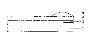
The electrical contact element depicted in Figure 1 has
a core part 1 in the form of a flat strip of an
iron/nickel alloy (e.g. Kovar). The core part 1 is
provided with a nickel layer 2 as a diffu~ion barrier
against the diffusion of the iron. Disposed on said .
nickel layer 2 is the adhesive layer 3. ~he adhesive
layer 3 comprises a silver/tin alloy, applied by electro-
plating, having a tin content of approximately 20 % by
weight, the remainder being silver. Disposed on a portion
o~ the adhesive layer 3 i~ the gold/~in alloy 40 Ths
- .... ~

gold~tin alloy 4 is placed as a sphere onto the adhesive
layer 3 and is then melted by means of a temperature
treatment at approximately 305C lasting for several
minutes.
To prevent diffusion of the iron into the adhesive layer
3, it is sllfficient to provide a nickel layer 2 having a
layer thickness of approximately 2 ~mO The adhesive layer
3 has a thickness of from approxim~tely 2 tn 4 ~m,
greater layer thicknesses also being possible, though
pointless for most applications.
A further embodiment is shown by Figure 2. In this case,
the soldered connection is provided on the end face of a
cylindrical core part 1. Disposed on khe end face, in the
same way as described above, are the nickel layer 2 and
the adhesive l~yer 3~ Onto this, covering the end facs,
the gold/tin alloy 4 is ~pplied in the form of a spheri-
cal ~egment whose contact surface corresponds to the end
face of the core part 1.
- . . : -,; .~: ,:. ,
, . ~, , , -:
- ~ . ,

Representative Drawing
A single figure which represents the drawing illustrating the invention.
Administrative Status

2024-08-01:As part of the Next Generation Patents (NGP) transition, the Canadian Patents Database (CPD) now contains a more detailed Event History, which replicates the Event Log of our new back-office solution.

Please note that "Inactive:" events refers to events no longer in use in our new back-office solution.

For a clearer understanding of the status of the application/patent presented on this page, the site Disclaimer , as well as the definitions for Patent , Event History , Maintenance Fee  and Payment History  should be consulted.

Event History

Description Date
Inactive: IPC from MCD 2006-03-11
Application Not Reinstated by Deadline 1997-05-12
Time Limit for Reversal Expired 1997-05-12
Deemed Abandoned - Failure to Respond to Maintenance Fee Notice 1996-05-13
Request for Examination Requirements Determined Compliant 1994-08-03
All Requirements for Examination Determined Compliant 1994-08-03
Application Published (Open to Public Inspection) 1994-01-22

Abandonment History

Abandonment Date Reason Reinstatement Date
1996-05-13
Owners on Record

Note: Records showing the ownership history in alphabetical order.

Current Owners on Record
W. C. HERAEUS GMBH
Past Owners on Record
GUNTER HERKLOTZ
Past Owners that do not appear in the "Owners on Record" listing will appear in other documentation within the application.
Documents

To view selected files, please enter reCAPTCHA code :


To view images, click a link in the Document Description column. To download the documents, select one or more checkboxes in the first column and then click the "Download Selected in PDF format (Zip Archive)" or the "Download Selected as Single PDF" button.

List of published and non-published patent-specific documents on the CPD .

If you have any difficulty accessing content, you can call the Client Service Centre at 1-866-997-1936 or send them an e-mail at CIPO Client Service Centre.


Document
Description 
Date
(yyyy-mm-dd) 
Number of pages   Size of Image (KB) 
Claims 1994-01-22 2 72
Drawings 1994-01-22 1 15
Abstract 1994-01-22 1 30
Cover Page 1994-01-22 1 29
Descriptions 1994-01-22 5 191
Representative drawing 1998-08-26 1 3
Fees 1995-04-13 1 60
Prosecution correspondence 1994-02-03 1 24
Prosecution correspondence 1994-04-22 2 44
Prosecution correspondence 1994-08-03 1 26
Prosecution correspondence 1994-07-07 2 36
Courtesy - Office Letter 1994-03-23 1 71
International preliminary examination report 1993-05-12 51 2,291