Note: Descriptions are shown in the official language in which they were submitted.
~J ~
~itle of_the I_ve tion
PHA8E DI8CRIMINATING CAPACITIVE ARRA~ 8EN80R 8Y8TEM
a_kqround of the Invention
Field of the Invention
This invention relates to a phase discriminating capacitive
sensor array system producing sensor signals which are phase and
amplitude controlled based on a frequency reference provided by
a single frequency stabilized oscillator.
Description of the Related Art
Capacitive sensor arrays are used in industry to sense the
proximity of an object. Conventionally, capacitive sensor arrays
have been provided with a circuit having a number of free running
oscillators, each corresponding to one of a number of sensor
elements in the array provided to sense the object. When one of
the sensors detected the object twas "pulled") the corresponding
oscillator experienced a change in frequency. The conventional
circuit recognized the object based on a change in capacitance
caused by the change in the frequsncy of the free running
oscillator. An example of such a conventional capacitive sensor
array system is fully described in An In-situ Evaluation of a
Capacitive_ Sensor Based Safety System__ for Automotive
Manufacturing Environment, by Don ~. Millard, published in Robots
13, Conference Proceedings, SME/RI, May 7-11, 1989.
In the conventional system described above, however, because
each of the free running oscillators provided for each sensor
element is susceptible to being "pulled" as described above, the
sensors must be placed far enough apart to ensure that the free
running oscillators in each sensor do not interact, couple and
- lock on to each other (cross talk). As a result, the range and
sensitivity of the conventional system has been limited by a
significant degree. Also, pixelized imaging has not been
possible due to the lack of proximal collocation of the sensor
elements.
Another disadvantage of the conventional capacitive sensor
array system has been that the multiple free running oscillators
have required that relatively wide band widths be provided for
the sensor electronics input bandwidths. These wide bandwidths
have resulted in increased noise and a decreased signal-to-noise
ratio. As a result of this disadvantage as well, the range and
sensitivity of the conventional system have been limited by a
significant degree.
Still another disadvantage of the conventional system has
been that frequency drift could not be prevented; since the
system depended on "pulling" the oscillator, frequency stabilized
oscillators, such as common crystal controlled oscillators, could
not be provided. As a result, frequency drift has posed a major
problem in the past, particularly due to increases in heat and
temperature.
An additional disadvantage potentially present in a
conventional capacitive sensor array system is that
"capaciflector" sensors could not be easily employed. In a
capaciflector sensor system individual shields are employed for
each sensor element, as disclosed in USP No. 5,166,679. As a
result, a capaciflector system using multiple free running
oscillators must have sufficient spacing to prevent cross talk
with the shields.
8ummary of the Invention
It is an object of the invention to provide a capacitive
sensor array system without limitation on the proximity of
adjacent sensor elements with capaciflector shields, without
cross talk between the sensor elements, and with a pixelized
imaging capability.
Another object of the invention is to provide a capacitive
- sensor array system with narrow band filtering and resulting
minimal noise and high signal to noise ration, without frequency
drift, and which can detect the proximity, closing speed and
edges of an object sensed by the sensor elements.
The above and other objects can be obtained by a phase
discriminating capacitive sensor array system which provides a
single free running oscillator which is stabilized to a fixed
frequency. Multiple sensor elements are provided for which the
single oscillator is a frequency reference. Multiple phase
control units, corresponding to the multiple sensor elements, are
also provided which control the phase and amplitude of the sensor
signals from the sensor elements to stay identical to that of the
frequency reference, and which determine the proximity of an
object by mea~suring the adjustment made to the sensor signals.
The phase control units may also determine the closing speed
of the object based on the rate of change of the adjustment,
and the edges of the object based on a sudden reduction in the
adjustment made.
According to the present invention then there is
provided a phase discriminating capacitive sensor array system
for detecting an object, comprising (a) a capacitive sensor
array having sensor elements to sense the object, each sensor
element producing a sensor signal; (b) a frequency stabilized
oscillator providing a frequency reference; and (c) phase
control means for controlling a phase and amplitude of each
sensor signal, and adjusting each sensor signal to correspond
to the frequency reference provided by said frequency
stabilized oscillator.
According to a further aspect of the present
invention, there is also provided a method of detecting an
object, comprising the steps of (a) sensing the object with
multiple capacitive sensor elements and producing a sensor
signal for each of the sensor elements; (b) providing a
common frequency reference for each of the sensor elements~;
and (c) adjusting the sensor signal from each of the sensor
elements to correspond to the common frequency reference.
According to yet another aspect of the present
invention, there is also provided a method of detecting an
object, comprising the steps of (a) sensing the object with
multiple sensor elements and producing a sensor signal for
each of the sensor elements; (b) providing a common frequency
reference for each of the sensor elements; and (c) adjusting
the phase and amplitude of the sensor signal from each of the
sensor elements to correspond to the common frequency
reference.
3a
Brief Description of the D~ g~
FIG. 1 is an overall block diagram of the phase
discriminating capacitive sensor array system of the present
invention;
FIG. 2 is a block circuit diagram of a phase control
unit shown in FIG. l; and
FIG. 3 is a flow chart of the control performed by
the controller shown in FIG. 2.
Detailed D~scription of the Preferrea Embodiments
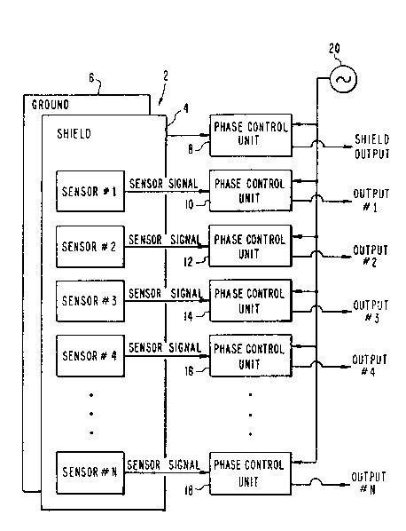
FIG. 1 shows an overall block diagram of the phase
discriminating capacitive sensor array system of the
invention, having an array 2 comprised of a common shield 4
on which sensor elements 1-N are provided, and a common ground
6. The shield 4 and sensor elements 1-N each output a sensor
signal to N phase control units 8, 10, 12, 14 and 16-18,
respectively. Each phase control unit maintains the phase and
amplitude of the sensor signal from each of the sensor
elements l-N, in accordance with a frequency reference
provided by a crystal controlled oscillator 20. The
oscillator is frequency stabilized to a common frequency
shared by the shield 4, ground 6 and sensor elements 1-N. Th,e
phase control units each produce an output signal (denoted
shield output, and outputs 1-N). These output signals
2S represent the voltage required to keep the sensor signals
provided by the corresponding sensor elements l-N at the same
frequency, phase and amplitude.
FIG. 2 is a block circuit diagram of any one of the
phase control units 8, 10, 12, 14, and 16-18. For example,
the phase control unit 10, which controls the sensor signal
from sensor element 1, and produces output 1, is shown. Th~
frequency reference from the oscillator 20 is passed through
a conventional phase shifter 22 and then through a
conventional gain control 24. The output of the gain control
drives a conventional resistor 26
2 ~
connected to the sensor element 1 and the input of a conventional
buffer amplifier filter 28.
The buffer amplifier filter 28 includes a narrow bandpass
filter at the frequency reference in order to remove a
significant amount of the ambient noise. Since the frequency is
fixed, the bandwidth is only as wide as the motion of the object
sensed by sensor 1, for example, 2 hertz. The narrow band
filtering is possible because the sensor element simply appears
as part of an impedance in a transmission line. This filtering
occurs upon input of the sensor signal to the phase control unit.
The output of the buffer amplifier filter 28 drives a
conventional phase comparator 30 and level comparator 32. The
outputs from these comparators are input to a controller 34,
which drives the phase shifter 22 and gain control 24 to maintain
the signal from sensor 1 identical to the frequency reference
from the oscillator 20.
When the sensor element 1 senses an object, its change in
capacitance changes the amount of adjustment required to be made
by the controller 34 to the sensor signal. This change in the
required amount of adjustment is reflected by a corresponding
change in voltage in the output signal (output 1) from the
controller 34. Thus, the change in voltage in output 1 indicates
the proximity of the object sensed by sensor 1. Also, the rate
of change in this voltage, which reflects the rate of change in
the required amount of adjustment, thus indicates the closing
speed of the object.
FIG. 3 is the flow chart of the control performed by the
controller 34. First, in step 36, the controller voltage VAHP
(used to set the initial voltage at the sensor element) and the
controller voltage VPH (used to set the initial phase at the
sensor element) are initialized. Also, the change in voltage av,
and the change in phase-induced voltage APH, which are expected
to result when the sensor element encounters the object, are
initialized based on an initial estimate for these values as
expected. Next, in step 38, the amplitude AMP of the sensor
signal is compared to the controller voltage VAMP which indicates
the initial sensor voltage. If AMP exceeds VAMP, then the
7 !1
controller voltage VAMP is adjusted in step 40 by adding the
change in voltage ~V of the sensor signal caused by the
capacitance change in the sensor element when the sensor element
senses an object. If, however, AMP does not exceed VAMP then VAMP
is adjusted in step 42 by subtracting the change in voltage AV.
In step 44, the phase PH of the sensor signal is compared
to controller voltage VPH (which indicate the initial sensor
phase). If PH exceeds VPH then the controller voltage VPH is
adjusted in step 46 by adding the phase induced voltage change
~PH. If, however, PH does not exceed VPH then VPH is adjusted in
step 48 by subtracting ~PH.
In step 50, ~V and ~PH are then recomputed based on a
software search which implements in iteration to converge these
values to within a specified range. Ideally, the specified range
takes into account the distance and speed of the object. In step
52, the controller voltages VAMP and VPH are output as the output
signal indicating the proximity and closing speed of the object.
Control then returns to step 38, and the above described steps
38-52 are continually repeated as appropriate.
As a result of maintaining the sensor signals to be
identical to the frequency reference provided by the oscillator
20, the sensor elements 1-N can be placed as closely together as
desired, so that cross talk between the sensor elements is
eliminated. The proximity and closing speed are measured by the
adjustment made to the sensor signals for each sensor element,
instead of by measuring an effect on a free running oscillator
for each sensor element, as in the conventional capacitive sensor
array system described above in the Background of the Invention.
Thus, multiple free-running oscillators do not need to be
provided corresponding to the multiple sensors, and cross-talk
is therefore not a problem.
Another advantage of maintaining the sensor signals to be
identical to the frequency reference is that the sensor elements
can be placed as closely to the shields as desired in a
"capaciflector" system, as described above. Thus, the sensor
elements 1-N can be provided on the single shield 4 as shown in
FIG. 2.
Also, because a narrow band bandpass filter is provided at
the frequency reference in the buffer amplifier filter 28, noise
is greatly reduced and the signal to noise ratio is improved,
thus improving the sensor range and sensitivity.
Additionally, the output signals which provide the voltage
indicative of the proximity and closing speed of the object can
be provided to a robot controller which interprets and acts on
the proximity and speed information accordingly. Also, as a
result of maintaining the sensor signals to be identical to the
frequency reference so that the sensor elements 1-N can be placed
closely together, a pixelized image of the object can be produced
using the output signals (shield output and outputs 1-N). Also,
the edges of the object can be detected based on a sudden
decrease in the voltages indicated by the output signals, which
indicates a fall off of the amount of adjustment applied to the
sensor signals for the sensor elements sensing the object at the
edge.
It should be noted that the output signals providing the
voltages indicative of the proximity, closing speed and edges of
an object, can be utilized in a number of applications including
but not limited to the robotics sensing and pixelized imaging
described above.